Wirebond crosstalk and cavity modes in large chip mounts for superconducting qubits
Abstract
We analyze the performance of a microwave chip mount that uses wirebonds to connect the chip and mount grounds. A simple impedance ladder model predicts that transmission crosstalk between two feedlines falls off exponentially with distance at low frequencies, but rises to near unity above a resonance frequency set by the chip to ground capacitance. Using SPICE simulations and experimental measurements of a scale model, the basic predictions of the ladder model were verified. In particular, by decreasing the capacitance between the chip and box grounds, the resonance frequency increased and transmission decreased. This model then influenced the design of a new mount that improved the isolation to -65 dB at 6 GHz, even though the chip dimensions were increased to 1 cm by 1 cm, 3 times as large as our previous devices. We measured a coplanar resonator in this mount as preparation for larger qubit chips, and were able to identify cavity, slotline, and resonator modes.
pacs:
06.60.Ei, 85.25.Am, 84.40.Dc, 84.30.Bv, 03.67.Lx1 Introduction
One promising approach toward quantum computation employs superconducting qubits [1]. Such qubits have been used to demonstrate simple gates [2, 3, 4, 5] and quantum algorithms up to three qubits [6, 7]. As additional qubits are added, they will require increasing room on each chip, eventually necessitating a larger chip and increasing numbers of microwave control lines [8]. It will thus become crucial to carefully engineer the mounting box, both because the increased density of input lines could lead to greater microwave crosstalk between the lines, and because stray cavity modes, which can present new modes for dissipation [9], can appear with larger mounts.
For superconducting microwave devices such as qubits and kinetic inductance detectors [10], most chip mounts have placed or glued a chip onto a metal base [11, 12, 13, 14, 15]. Wirebonds are then used to connect the chip ground plane and pads to the external mount’s ground plane and feedlines, which are typically made from a circuit board.
In this paper, we show that although such a mount may work well for the current generation of small chips, increasing the chip size will cause the ground connection to fail at microwave frequencies. Specifically, crosstalk will increase because of increased capacitance from the chip to mount ground, contrary to the usual assumption that tying the grounds together with capacitance improves their connection. With a simple ladder model, we explicitly show this capacitance introduces a traveling wave mode between the chip and mount grounds, thereby giving a continuum of resonance modes which decouples the two grounds and provides a mechanism for large crosstalk.
To understand the effects from the wirebonds and mount, we first develop a semiquantitative model, and then discuss experimental tests using a simple scaled-up system. The predictions of this model were then used to design a new sample mount with a reduced capacitance between the mount and chip ground planes. An actual resonator device was then measured for this design. This mount accommodates a chip three times the area of our current generation of qubits; with this increase in size, and with added cavities to reduce the capacitances between the box and chip ground planes, we identified sources of cavity and chip modes up to 20 GHz.
2 Wirebond Crosstalk
2.1 Circuit Model
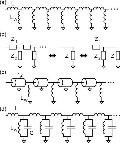
When mounting a microwave device, it is necessary to ensure that the chip is well grounded to the mounting box. This may be achieved using many short, closely-spaced wirebonds around the edge of the die. To understand the effect of this network, we consider the simple model illustrated in Figure 1, which will later be experimentally verified. Here, the grounding wirebonds between an input and an output feedline are considered to be an impedance ladder, with a node at each point where a wirebond connects to the chip ground plane.
Each wirebond can be modeled as a wire having inductance between each node and the box ground. This inductance is proportional to the length of the wirebond, with a proportionality constant of approximately 1 nH/mm for typical wirebonds due to ground plane effects [16]. The length of the wirebond can be modeled to be approximately the minimum possible length for the wirebonds, the distance between the chip and the edge of the mount. In addition, the edge of the chip ground plane gives an inductance between two adjacent nodes. Its magnitude is for an edge inductance per unit length and distance between adjacent wirebonds. We assume the corresponding edge inductance from the mount ground plane is negligible because adjacent nodes are connected through the bulk. These two types of inductances give rise to a “ladder model” for the interface between the chip and mount ground planes, as illustrated in Figure 1(a).
We model microwave crosstalk as coming from voltage propagating along the ground nodes on the chip. The crosstalk between two ports can then be solved geometrically by following the approach [17] illustrated in Figure 1(b), where the impedance looking into the ladder is given by and is independent of node position. The ratio of voltages between adjacent nodes of the inductor ladder is
| (1) | |||
| (2) |
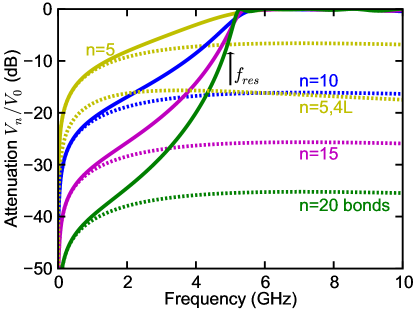
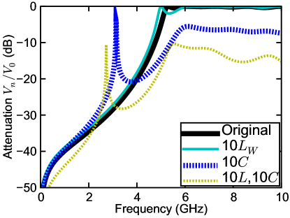
As the inductance ratio increases, the voltages along the nodes are more quickly suppressed. This implies that should be reduced as much as possible by keeping wirebonds short. The voltage ratio between widely spaced points is given by a geometric sequence . Note that while increasing the distance between bonds increases and thus reduces , it also reduces the number of bonds . As illustrated in Figure 2, for increased attenuation it is more advantageous to have a high density of wirebonds than to space fewer wirebonds over the same length of ground plane.
Capacitance between the ground plane of the chip and the mount must also be included in the model. For a chip placed on a metal plane, this capacitance is distributed to all points on the ground plane of the chip, but for simplicity we treat it as being connected along the edge of the chip. This capacitance, along with the inductance , is distributed over the length between wirebonds, giving a transmission line as illustrated in Figure 1(c). By employing a model [18], the capacitance can be divided between the wirebond nodes as lumped elements. As with parallel plate or coplanar capacitors, this capacitance is proportional to the distance between adjacent wirebonds, giving for capacitance per unit length . With these assumptions, the chip mount is represented by the model illustrated in Figure 1(d), where capacitance is placed in parallel to the bond-wire inductance. The ratio of voltages between adjacent nodes can be solved in the same manner as for (1), but here
| (3) |
When adding capacitance, the important result is that the wirebond inductance resonates with the capacitance at a frequency , resulting in a loss of shunting from the wirebonds. At (and above) this frequency, signals propagate along the chip ground without being strongly attenuated.
To account for the finite size of the ladder, we also simulated this circuit with SPICE for various numbers of bonds and ratios of inductance and capacitance. These simulations confirmed quantitatively the predictions of the simple model, particularly that the transmission approaches unity above and increasing numbers of bonds attenuate voltage more strongly at frequencies below the resonance. Figure 2 shows a typical simulation result, corresponding to model A of Table 1.
We also checked the assumption of a lumped model for the ground inductance and capacitance by simulating short lengths of transmission lines, as illustrated in Figure 1(c). By calculating the transmission matrix [19], we solved for the voltage ratios between nodes and found that the resonance frequency satisfies
| (4) |
When solved numerically, we found predictions changed less than 5% as compared to the lumped model, indicating that the lumped model is adequate for the analysis presented here.
2.2 Experimental Setup and Analysis
| overlap | (LE) | (TL) | |||||||||
|---|---|---|---|---|---|---|---|---|---|---|---|
| (mm) | (mm) | (mm) | (fF/mm) | (nH/mm) | (nH) | (nH) | (fF) | (GHz) | (GHz) | ||
| A | 2.5 | 2.5 | 5.1 | 174.9 | 0.22 | 0.56 | 2.54 | 0.22 | 444 | 4.74 | 4.69 |
| B | 2.5 | 2.5 | 2.5 | 114.6 | 0.29 | 0.74 | 2.54 | 0.29 | 291 | 5.85 | 5.78 |
| C | 2.5 | 2.5 | 0.0 | 55.9 | 0.43 | 1.09 | 2.54 | 0.43 | 142 | 8.38 | 8.23 |
| D | 2.5 | 2.5 | -2.5 | 32.4 | 0.58 | 1.47 | 2.54 | 0.58 | 82 | 11.0 | 10.75 |
| E | 2.5 | 5.1 | 2.5 | 114.6 | 0.29 | 1.47 | 2.54 | 0.58 | 582 | 4.14 | 4.04 |
| F | 2.5 | 1.3 | 2.5 | 114.6 | 0.29 | 0.74 | 2.54 | 0.15 | 145 | 8.28 | 8.23 |
| G | 5.1 | 2.5 | 2.5 | 114.0 | 0.30 | 0.76 | 5.08 | 0.15 | 290 | 4.15 | 4.12 |
| H | 1.3 | 2.5 | 2.5 | 117.2 | 0.28 | 0.71 | 1.27 | 0.56 | 298 | 8.18 | 8.00 |
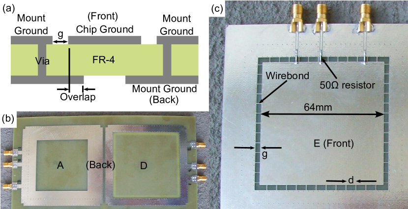
To verify semiquantitatively the predictions of this ladder model, we built a scale model of a chip, its wirebonds, and a mount, as illustrated in Figure 3. The scale models were commercially fabricated on FR-4 circuit board with double sided-copper and plated vias. The effects of capacitance from the chip to the mount were modeled by varying amounts of metal overlap between the top and bottom sides of the board. We assumed that the wirebond inductance scaled as 1 nH/mm multiplied by the gap between the two ground planes, and that the edge inductance and capacitance scaled as the distance between adjacent wirebonds.
On the top side, the chip was modeled by a 64 mm metal square, ten times larger than our group’s standard qubit chips. A gap of width separated this ground plane from that of the mount ground. Stretching across the gap were 0.25 mm wide metal traces that simulated the wirebonds. To measure the voltage attenuation down the chip, we included three signal leads, separated by 13 mm and 23 mmn, that were connected by a coplanar waveguide to a 50 resistor placed across the gap to the chip ground plane. The ground plane on the back side of the circuit board was connected with vias to the ground plane of the top mount.
As illustrated in Table 1, we used a default distance of 2.5 mm for the gap between the front- and back-side ground planes, the distance between adjacent bonds, and the overlap distance between the front side chip and the back side ground plane. These three parameters were changed for the eight different models. For each model, the COMSOL multiphysics package [20] was used to calculate the edge inductance and capacitance per unit length; these parameters, along with the inductances and capacitances derived from these values, are also included in Table 1.
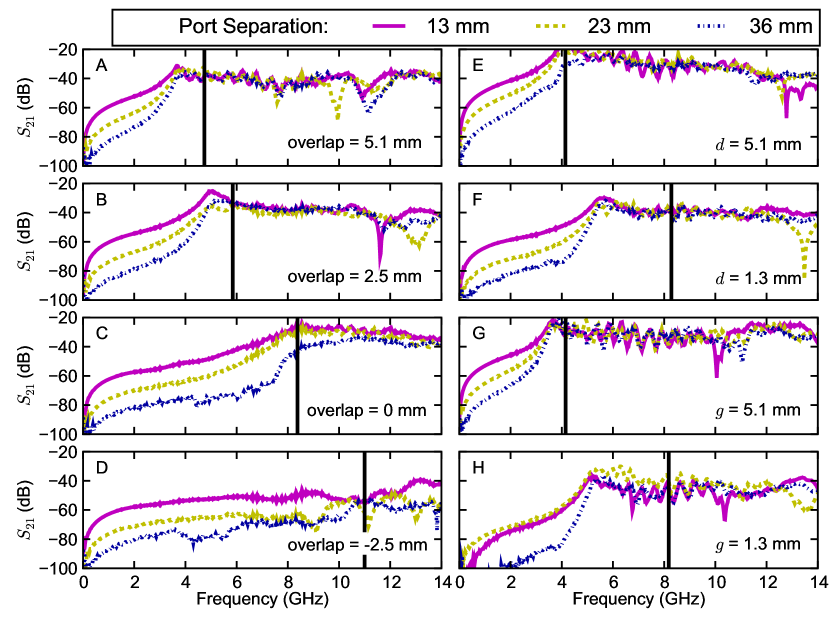
We used a vector network analyzer at room temperature to measure the scattering matrix for these scale models. By measuring between pairs of the three connectors, we were able to determine attenuation for three different lengths. The resulting traces are shown in Figure 4.
As predicted by the frequency dependence of the model, we observed rolloff at very low frequency, then rising transmission until a resonance frequency, after which the transmission remains high. Below the resonance frequency, we observed increased attenuation for increased number of wirebonds, with frequency dependence and magnitudes in qualitative agreement with theory. Loss from the circuit board was important above approximately 5 GHz, as expected for an FR-4 substrate and copper metallization. The predicted resonance frequency is shown as a vertical black line in all plots, which shows reasonable agreement between experiment and theory.
Panels A-D show that the resonance frequency increases with decreasing ground capacitance, as expected by theory. Changing the wirebond spacing (panels E-F) and wirebond length (panels G-H) show a change in frequency in the correct direction. The change is smaller than predicted for panels F and H, probably due to mutual inductance between the bonds.
With some confidence in the basic model, it is possible to extract useful information about practical design issues, such as the effect of nonuniform wirebonding, which occurs as a result of unsuccessful wirebonds. Using SPICE simulations, we modeled a gap in the wirebonds with an increased inductance and capacitance at one location in the ladder. Surprisingly, the lower-frequency resonance at this one location produces transmission through the entire ladder, leading to a peak in the transmission as seen in Figure 5. This indicates that wirebonds should be made as uniformly as possible all the way around the chip. However, note that even with a gap of bond spacings, the resonance frequency is only reduced by a factor of two. For the case of long wirebonds, the resonance frequency is lowered at one spot in the ladder, but does not lead to a significantly lowered resonance in the transmission. In contrast, increasing the capacitance locally does lower the resonance frequency. In summary, small irregularities in wirebonding do not appear to be critical to the mount performance.
3 Mount for large chips
We used this model to design a new mount and to calculate its expected performance. To determine the effects of wirebond spacing and length, COMSOL was used to calculate the inductance and capacitance for a mount with different wirebond configurations. We assumed the mount had ground planes 1.4 mm above and 1.9 mm below the chip. We considered the effect of various bond spacings with a gap between the box and chip ground plane of m and a bond length of m, which accounts for the arching of the bond. For a bond spacing of m, giving a total of 20 bonds per cm, we calculated GHz and , for an attenuation of 5.2 dB per bond (104 dB/cm). A bond spacing of m, for a total of 50 bonds per cm, gives GHz and , and an attenuation of 3.3 dB per bond (167 dB/cm). These results show that acceptable attenuation is possible using parameters that are experimentally feasible.
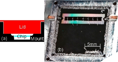
A new mount was designed for chips with 1 cm sides to achieve these wirebonding parameters and to experimentally test performance. As illustrated in Figure 6, we used many short wirebonds between the chip and the mount to reduce crosstalk. Stray capacitance was minimized by designing a box with cavities both above and below the chip. The box was made from aluminum to shield stray magnetic fields when the devices are cooled to temperatures below 100 mK.
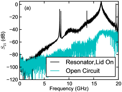
We used a coplanar resonator chip to quantify the mount performance. The resonators were optically patterned 150 nm thick aluminum films sputtered on silicon. The chip mount was cooled by an adiabatic demagnetization refrigerator to approximately 100 mK. The results from resonator measurements are plotted in Figure 7, which have the transmission magnitudes normalized by removing cable attenuation in order to express the results as a mount response.
As illustrated in Figure 7(a), we measured a transmission of -65 dB at 6 GHz, only somewhat larger than coming from open-circuit transmission without the mount. The noise in the data comes from the noise floor of the network analyzer.
4 Identification of spurious modes
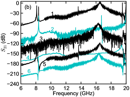
As shown in Figure 7(b.1), we observed several resonance modes when the chip was measured at 100 mK. This is partly due to the large size of the mount, which has dimensions of 1 cm, approximately a half-wavelength for the highest frequencies studied here. In order to identify the modes, we performed several additional experiments.
One test was to measure the resonator at room temperature, as shown in Figure 7(b.3) and (b.4). The presence of resonance modes at 16 GHz and at 19.6 GHz indicates these are cavity modes, as the lack of superconductivity precludes a chip resonance mode. As a further test, we then either removed the lid (see Figure 7(b.2)) or placed Eccosorb LS-26 microwave-absorbing foam inside the sample mount lid (data not shown), and observed the disappearance of the 16 GHz resonance leaving only the 19.6 GHz peak. We interpret this as the 16 GHz peak coming from a cavity resonance between the chip and mount lid. The 19.6 GHz peak probably comes from the smaller cavity below the chip.
Slotline modes are another source of undesirable resonances, which correspond to having unequal voltages on the ground planes on either side of the coplanar resonator. To identify these modes, a resonator chip was fabricated the same as the coplanar resonator but with no center trace; these measurements are plotted in Figure 7(b.5), where we find resonance modes at 8.1 GHz, 13.6 GHz, and 20 GHz. Since these have not previously been identified as cavity modes, we identify them as slotline mode. Note that their frequency ratios are close, but not equal, to 1:2:3. These modes may be suppressed by airbridge wiring spanning the coplanar leads, which forces the voltages on either side to be equal. As illustrated in Figure 6, we emulated this by spanning all coplanar traces with about 30 wirebonds, although we later found that 9 wirebonds sufficed. When doing so, we found these three slotline modes were all suppressed, as shown in Figure 7(b.6).
We identify the mode at 8.4 GHz as the coplanar resonator mode, since it is not a cavity or slotline mode. This matches the design value of about 9 GHz. This was further confirmed by cooling through the transition temperature while applying a 2.5 G magnetic field; as this value exceeds the critical field for the 6 m width traces for flux trapping [21], one expects a significant decrease in the factor [22, 23]. By following the approach in [24] for measuring , we found this mode dropped in by a factor of 10, whereas other modes were only degraded by at most a factor of two. We also found the characteristic field size for degradation of was consistent with the width of the resonator’s center trace.
Finally, when the lid was removed, an additional resonance mode was present at 16.7 GHz, as shown in Figure 7(b.2). With the lid attached, the 16 GHz cavity mode had masked this additional mode. The for this mode decreased by a more than a factor of 10 when field cooling, implying this is a coplanar mode. This is consistent with expectations since the frequency of this mode is almost twice that of the fundamental coplanar mode.
We note that increasing the chip size beyond 1.5 cm will lower the frequency of cavity modes to that near the qubit, and issue that will clearly have to be addressed in future research. Since we observed that damping reduces cavity crosstalk in Figure 7(b.4), we expect that efficient damping of these modes will enable the construction of large chip mounts with low crosstalk.
5 Conclusion
In conclusion, we have modeled crosstalk in a microwave chip mount as arising from non-zero wirebond inductance. A impedance ladder model has been developed that can predict the performance on the grounding, and was experimentally verified with a scale model. Our calculations indicate that stray transmission falls off at low frequencies with increasing wirebond density, and reaches near unity at a resonance frequency determined by the wirebond length and the stray capacitance between the chip and mount grounds. Hence, to improve the mount, it is necessary to use a high density of short grounding wirebonds and to decrease stray capacitance by using a mount without a ground plane under the chip.
A new chip mount was developed with this improved design in mind. We were able to characterize various resonances, including coplanar, cavity, and slotline modes. The stray coupling was reduced to about -65 dB at 6 GHz. This new mount is compatible with centimeter-sized chips for future qubit devices and points the way for even large chip sizes.
References
References
- [1] Clarke J and Wilhelm F K 2008 Nature 453 1031–42
- [2] Yamamoto T, Pashkin Y A, Astafiev O, Nakamura Y, and Tsai J S 2003 Nature 425 941–4
- [3] Plantenberg J H, de Groot P C, Harmans C J P M, and Mooij J E 2007 Nature 447 836–39
- [4] DiCarlo L, Chow J M, Gambetta J M, Bishop L S, Johnson B R, Schuster D I, Majer J, Blais A, Frunzio L, Grivin S M, and Schoelkopf R J 2009 Nature 460 240–4
- [5] Yamamoto T, Neeley M, Lucero E, Bialczak R C, Kelly J, Lenander M, Mariantoni M, O’Connell A D, Sank D, Wang H, Weides M, Wenner J, Yin Y, Cleland A N, and Martinis J M 2010 Phys. Rev. B 82 184515
- [6] Neeley M, Bialczak R C, Lenander M, Lucero E, Mariantoni M, O’Connell A D, Sank D, Wang H, Weides M, Wenner J, Yin Y, Yamamoto T, Cleland A N, and Martinis J M 2010 Nature 467 570–3
- [7] DiCarlo L, Reed M D, Sun L, Johnson B R, Chow J M, Gambetta J M, Frunzio L, Girvin S M, Devoret M H, and Schoelkopf R J 2010 Nature 467 574–8
- [8] Mariantoni M, Wang H, Bialczak R C, Lenander M, Lucero E, Neeley M, O’Connell A D, Sank D, Weides M, Wenner J, Yamamoto T, Yin Y, Zhao J, Martinis J M, and Cleland A N 2010 Photon shell game in three-resonator circuit quantum electrodynamics Preprint arXiv:1011.3080
- [9] Schuster D I, Sears A P, Ginossar E, DiCarlo L, Frunzio L, Morton J J L, Wu H, Briggs G A D, Buckley B B, Awschalom D D, and Schoelkopf R J 2010 Phys. Rev. Lett. 105 140501
- [10] Mazin B A 2009 AIP Conf. Proc. 1185 135–42
- [11] Cicak K, Allman M S, Strong J A, Osborn K D, and Simmonds R W 2009 IEEE Trans. Appl. Supercond. 19 948–52
- [12] Deppe F, Mariantoni M, Menzel E P, Saito S, Kakuyanagi K, Tanaka H, Meno T, Semba K, Takayanagi H, and Gross R 2007 Phys. Rev. B 76 214503
- [13] Mazin B A, Sank D, McHugh S, Lucero E A, Merrill A, Gao J, Pappas D, Moore D, and Zmuidzinas J 2010 Appl. Phys. Lett. 96 102504
- [14] Frunzio L, Wallraff A, Schuster D, Majer J, and Schoelkopf R 2005 IEEE Trans. Appl. Supercond. 15 860–3
- [15] Palacois-Laloy A, Nguyen F, Mallet F, Bertet P, Vion D, and Esteve D 2008 J. Low Temp. Phys. 151 1034–42
- [16] Grover F W 1912 Bulletin of the Bureau of Standards 8 150
- [17] Feynman R P, Leighton R B, and Sands M L 1964 The Feynman Lectures on Physics vol 2 (Reading, MA: Addison-Wesley) sec 22-6
- [18] Johnson H and Graham M 2003 High-Speed Signal Propagation: Advanced Black Magic (Upper Saddle River, NJ: Prentice Hall) sec 3.4.2
- [19] Pozar D M 2004 Microwave Engineering ed 3 (Hoboken, NJ: Wiley) sec 4.4
- [20] COMSOL AB 2007 (Stockholm)
- [21] Stan G, Field S B, and Martinis J M 2004 Phys. Rev. Lett. 92 097003
- [22] Song C, Heitmann T W, DeFeo M P, Yu K, McDermott R, Neeley M, Martinis J M, and Plourde B L T 2009 Phys. Rev. B 79 174512
- [23] Wang H, Hofheinz M, Wenner J, Ansmann M, Bialczak R C, Lenander M, Lucero E, Neeley M, O’Connell A D, Sank D, Weides M, Cleland A N, and Martinis J M 2009 Appl. Phys. Lett. 95 233508
- [24] O’Connell A D, Ansmann M, Bialczak R C, Hofheinz M, Katz N, Lucero E, McKenney C, Neeley M, Wang H, Weig E M, Cleland A N, and Martinis J M 2008 Appl. Phys. Lett. 92 112903