Electrodynamic Response of the Charge Ordering Phase:
Dielectric and Optical Studies of -(BEDT-TTF)2I3
Abstract
We report on the anisotropic response, the charge and lattice dynamics of normal and charge-ordered phases with horizontal stripes in single crystals of the organic conductor -(BEDT-TTF)2I3 determined by dc resistivity, dielectric and optical spectroscopy. An overdamped Drude response and a small conductivity anisotropy observed in optics is consistent with a weakly temperature dependent dc conductivity and anisotropy at high temperatures. The splitting of the molecular vibrations evidences the abrupt onset of static charge order below K. The drop of optical conductivity measured within the plane of the crystal is characterized by an isotropic gap that opens of approximately 75 meV with several phonons becoming pronounced below. Conversely, the dc conductivity anisotropy rises steeply, attaining at 50 K a value 25 times larger than at high temperatures. The dielectric response within this plane reveals two broad relaxation modes of strength and , centered at MHz and MHz. The anisotropy of the large-mode (LD) mean relaxation time closely follows the temperature behavior of the respective dc conductivity ratio. We argue that this phason-like excitation is best described as a long-wavelength excitation of a bond-charge density wave expected theoretically for layered quarter-filled electronic systems with horizontal stripes. Conversely, based on the theoretically expected ferroelectric-like nature of the charge-ordered phase, we associate the small-mode (SD) relaxation with the motion of domain-wall pairs, created at the interface between two types of domains, along the and axes. We also consider other possible theoretical interpretations and discuss their limitations.
pacs:
71.45.-d, 77.22.Gm, 71.30.+h, 78.30.-jI Introduction
The competition between the tendency of electrons to delocalize and the presence of electron-electron interaction, electron-phonon interaction – often combined with spin-phonon interaction – is the origin of the extremely rich phase diagrams in the condensed matter systems with reduced dimension.Fulde93 ; MC04 Among the most intriguing phenomena found in these systems are broken-symmetry phases like charge- and spin-density waves (CDW, SDW), charge orders (CO), antiferromagnetic, spin-Peierls phases and superconductivity. These phases show a large variety of nonlinear properties and complex dynamics, including collective excitations.Gruener88 ; Littlewood87 ; Cava85 ; VuleticPR ; Dressel09 . While the conventional (2) CDW implies periodically modulated charge density and is caused by the electron-phonon interaction, the charge modulation of Wigner-crystal type, often called charge ordering, originates from strong on-site Coulomb repulsion . Thus, the CO is most commonly thought of as the alternating localized charge of different valencies arranged in a crystal lattice. In particular, a wealth of CO phenomena with charge disproportionation is found in organic conductors characterized by different anisotropic networks. These include quasi-one-dimensional (TMTTF) (Ref. Monceau01, ), (DI-DCNQI)2Ag (Ref. Kanoda07, ) and quasi-two-dimensional conductors based on the BEDT-TTF [bis(ethylenedithio)tetrathiafulvalene] molecule: such as -(BEDT-TTF)2RbZn(SCN)4 and -(BEDT-TTF)2I3.Takahashi06 It is notable that these systems have a quarter-filled conduction band and due to that not even the large values of on-site repulsion with respect to the electron hopping are sufficient to transform the ground state from metallic to insulating. Rather, the inter-site Coulomb interaction is required to stablize a Wigner-crystal type phase.Seo06 Although CO features seem to point directly toward full localization of charges and their alternating arrangements, some theoretical studies dispute this conventional view indicating that a delocalized CDW picture might also be relevant to some CO, e.g., like the one in -(BEDT-TTF) materials.Clay02
-(BEDT-TTF)2I3, the first organic material to show highly conductive properties in two dimensions,Bender84-108 is also one of the most prominent examples of charge order among 2D organic conductors. This system displays a rich temperature-pressure phase diagram with a number of intriguing quantum phenomena ranging from superconductivity,Tajima02 , charge order,Takahashi06 persistent photoconduction,Tajima05 photoinduced phase transition,Iwai07 nonlinear ultrafast optical response,Yamamoto08 and zero-gap semiconductivityMori10 characterized by Dirac cones and massless Dirac fermions.Tajima07 ; Tajima09 In addition, recently a first successful observation was reported of correlated electron motion in the light-matter interaction leading to the photo-induced insulator-to-metal transition.Kawakami10
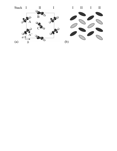
The triclinic crystal structure is an alternation of insulating anion (I) layers and conducting layers of donor molecules (BEDT-TTF0.5+ on average). The BEDT-TTF molecules form a herring-bone structure and are organized in a triangular lattice with two types of stacks. At room temperature stack I is weakly dimerized and composed of crystallographically equivalent molecules A and A′, while the stack II is a uniform chain composed of B and C molecules [see Fig. 1(a)]. Thus the unit cell contains four BEDT-TTF molecules. At high temperatures the system is a semimetal with small electron and hole pockets in the Fermi surface.Bender84 ; MoriCL84 A slight but noticable charge disproportionation is observed already at room temperature, indicating that CO gradually develops as the temperature is reduced towards .Kakiuchi07 ; Moroto04 . As demonstrated by nuclear magnetic resonance (NMR)Takano01 and synchrotron x-ray diffraction measurements,Kakiuchi07 charge order at long length scales develops fully below the metal-to-insulator phase transition K. At the conductivity drops by several orders of magnitude and a temperature-dependent gap opens in charge and spin sector which indicates insulating and diamagnetic nature of the ground state. x-ray diffraction measurements indicate subtle structural changes at . There are no translations of molecules, only a shift in dihedral angles (angles between molecules of two neighboring stacks) is observed. This results in breaking of inversion symmetry between A and A′ sites, with space group changing from P to the P1, and also allows for crystal twinning in the low-temperature acentric structure. The variations in dihedral angles cause an appreciable 2D modulation of overlap integrals between the BEDT-TTF sites.Kakiuchi07 Finally, molecular deformations are observed which are at the origin of charge disproportionation. Estimated charge values of the molecules A, A′, B and C are , , and , respectively. The exact site assignment is not settled yet, since these values differ slightly from those found in the NMR, vibrational infrared and Raman spectroscopy, and anomalous x-ray diffraction measurements.Takano01 ; Moldenhauer93 ; Dressel04 ; Drichko09 ; Wojciechowski03 ; Kakiuchi07 Nevertheless, all these experiments consistently indicate that the charge order comprises “horizontal” charge stripes of charge-poor (CP) sites, the A′ and C molecules, and charge-rich (CR) sites (A and B molecules) along the crystallographic axis, as depicted in Fig. 1(b). Contrary to the conventional view of the CO as an alternation of localized charges, experimental x-ray data indicate that a delocalized CDW-like picture might be a more appropriate description of the CO stabilized in this system.
There have been some previous attempts to find evidence of collective response in -(BEDT-TTF)2I3. More than fifteen years ago, preliminary measurementsDressel94 indicated the existence of a broad relaxation in radio-frequency range with a large dielectric constant of the order of as well as sample-dependent nonlinearities. However, no conclusive interpretation could be given at that time. These experiments need to be revisited and more detailed ones with electric fields along different crystallographic directions have to be added in order to shed more light on the electrodynamics of the charge-ordered state. Recently anisotropic voltage oscillations have been observed that are associated with nonlinear conductivity.Tamura10 Such a phenomenon closely resembles the collective sliding motion of density waves in quasi-one-dimensional conductors,Gruener88 which makes it yet another result to raise the question of similarities and differences between conventional density waves and CO found in 2D systems. At the time of writing of this paper, Yue et al.Yue10 presented a new detailed infrared and Raman study in the metallic and CO phase of -(BEDT-TTF)2I3.
In an attempt to clarify several issues mentioned above we have undertaken an investigation of electrodynamic response in the normal phase and ground state of the layered organic conductor -(BEDT-TTF)2I3. We have performed comprehensive optical investigations in all three crystallographic directions, as well as dc and ac conductivity-anisotropy measurements on carefully oriented single crystals of -(BEDT-TTF)2I3. A brief report of this investigation has previously been published.Ivek10 Our results demonstrate a complex and anisotropic dispersion in the charge-ordered state in contrast to an almost isotropic and temperature-independent charge response at high temperatures. The abrupt onset of static charge order below K is signaled by a splitting of molecular vibrations and a dramatic drop of the optical conductivity. Its anisotropy does not change much in contrast to anisotropy of dc conductivity which rises steeply with decreasing temperature. Charge redistribution detected in the CO phase corresponds nicely to the one estimated from the x-ray data.Kakiuchi07 Similar to the Peierls CDW state, we observe long-wavelength charge excitations with an anisotropic phason-like dispersion, which surface as broad screened relaxation modes along the - and -axes of the BEDT-TTF planes. In addition, we detect short-wavelength charge excitations in the form of domain-wall pairs, created due to inversion symmetry breaking, which are less mobile and induce a much weaker polarization, again along both crystallographic axes. Possible theoretical interpretations are discussed and arguments are given that the nature of the horizontally-striped CO phase is a cooperative bond-charge density wave rather than a fully localized Wigner crystal.
II Sample characterization and experimental methods
DC resistivity was measured between room temperature and 40 K by standard four-contact technique. In the frequency range 0.01 Hz–10 MHz the spectra of the complex dielectric function were obtained from the two-contact complex conductance measured by two setups. The low-frequency, high-impedance setup covers the 0.01 Hz – 3 kHz range. ac voltage signal is applied to the sample, the current response is transformed to voltage by a Stanford Research Systems SR570 current preamplifier and detected using a dual-channel digital lock-in Stanford Research Systems SR830. At higher frequencies (40 Hz – 6 MHz) an Agilent 4294A impedance analyzer with virtual ground method was used. Even though the impedance analyzer reaches frequencies up to 110 MHz, we are limited to approximately 6 MHz by cable length. The applied ac signal levels, typically 50 mV (1 V/cm), were well within the linear response regime (upper bound verified to be at least 6 V/cm). The results obtained by both methods agree in the overlapping frequency range. In dielectric measurements a background contribution of stray capacitances is always present due to cabling and sample holder construction. In order to account for and remove these influences, we have routinely subtracted the open-circuit admittance from all measured sample admittances. The background capacitance of our setup amounts to 350 fF at all measured temperatures. At frequencies 10–10000 cm-1 the complex dielectric function was obtained by a Kramers-Kronig analysis of the temperature-dependent infrared reflectivity measured by Fourier transform spectroscopy applying common procedure.Dressel04
The samples under investigation are flat, planar high-quality single crystals. As a rule, the pronounced sample surface is in the plane of the crystal structure. The -axis of the crystal corresponds to the direction perpendicular to sample plane. The reflectivity measurements were performed on as-grown surfaces; for our -axis investigation we employed an infrared microscope.
Contacts for dc and ac conductivity measurements were made by applying carbon paint directly to sample surface. On our first studied single crystal contacts have been prepared parallel to sample edges without prior orienting the sample. After dc and ac conductivity measurements, the orientation of contacts was determined to be approximately along (diagonal) direction by taking the x-ray back-reflection Laue photograph with the beam direction perpendicular to the largest facets of the sample. OrientExpress3.3 softwareMilat was applied to simulate the recorded flat back reflection patterns. Additional experiments were conducted on needle-like samples cut from one single crystal that was oriented by recording the mid-infrared spectra. The needles were cut along in-plane axes which ensured that the orientation of electric field is along one of the axes. The dc and ac conductivity on those samples was measured parallel to the -axis (perpendicular to stripes; along this direction CR and CP sites alternate) and parallel to the -axis (along the stripes).
With scrutiny we ruled out any influence of extrinsic effects in the dielectric spectroscopy measurements, especially those due to contact resistance and surface layer capacitance. Of the two relaxation modes detected in the dielectric response, the smaller one has a temperature-independent relaxation time, thus it can be identified as an intrinsic property of the sample. On the other hand, the larger dielectric mode bears features which might indicate a Maxwell-Wagner-like relaxation at the contactsLunkenheimer02 and requires a thorough verification of contact quality. With this in mind, we performed dc resistance measurements in the standard four- and two-contact configurations. Taking into account the difference in geometry between contacts in these two configurations, the four-point resistance can be scaled and subtracted from the two-point resistance in order to estimate contact resistance () vs. sample bulk resistance (). In the insulating phase our samples feature a gradually rising ratio, from 0.1 just below the transition up to the order of 10 at temperatures below 50 K. However, independent of the changes in ratio, the strength of dielectric response remained approximately constant and finite throughout the insulating regime proving that the observed behavior of measured capacitance is governed predominantly by sample bulk response. Only the dielectric spectra in the immediate vicinity of were under influence of instrument artefact and therefore disregarded. Namely, above 135 K the sample conductivity becomes greater than the imaginary part of admittance by a factor of 1000 or more in the whole range of frequency , an instrument limit beyond which no meaningful measurements of capacitance can be made.
III Results and analysis
III.1 Optics
Despite the numerous reports on the optical properties of -(BEDT-TTF)2I3,Sugano85 ; Meneghetti86 ; Yakushi87 ; Yue10 ; Zamboni89 ; Zelzny90 ; Gartner91 ; Moldenhauer93 ; Dressel94 ; Drichko09 ; Clauss09 a few aspects of the development right at or below the charge-order transition are worthwhile to be reconsidered in the present context. Here we concentrate on two issues. The first is the conductivity and reflectivity in the highly-conducting () plane at the metal-to-insulator phase transition which yield information on the anisotropy and the energy gap. The second issue concerns the redistribution of charge on the molecular sites that can be monitored via the vibrational features and their evolution on cooling. Vibrational spectroscopy with light polarized is most sensitive to characterize charge order.Dressel04 ; Yamamoto05 In addition, we present and discuss vibrational features of the BEDT-TTF molecule in metallic and the CO state seen with light polarized and .
III.1.1 Electronic contributions
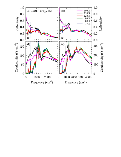
The experimentally accessible frequency range extends from 10 to 5000 cm-1 and covers the bands formed by the overlapping orbitals of neighboring molecules. Fig. 2 shows the optical properties for the two polarizations and in the highly conducting plane at different temperatures above and below . The optical spectra are dominated by a broad band in the mid-infrared in both directions that is different in strength by about a factor of 2. A shoulder in , which shows up as a pronounced dip in the conductivity spectra around 1450 cm-1, is due to the strong electron-molecular vibrational (emv) coupling of the (Ag) mode.Dressel04
Overall behavior and anisotropy.
Although the reflectivity exhibits a metallic response at ambient temperatures leading to a finite conductivity, no Drude-like response of the quasi-free carriers can be separated from the wing of the mid-infrared band [Fig. 2(b), (d) and Fig. 3]. Hence the weakly temperature-dependent conductivity above the metal-insulator transition is described by an overdamped Drude response, i.e., a small spectral weight compared to the large scattering rate.
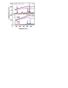
Upon decreasing the temperature from 300 K down to , the reflectivity slightly increases due to reduced phonon scattering. In the CO state, the far-infrared reflectivity drops dramatically and the corresponding optical conductivity decreases as the energy gap opens in the density of states (Fig. 3). The spectral weight shifts to the mid-infrared range where it piles up in a band with maxima around 1500 cm-1 for (parallel to the stacks) and 2000 cm-1 for (perpendicular to the stacks).note2 When screening by the conducting charge carriers is reduced at , the Fano-shaped antiresonances in the conductivity due the emv coupled molecular vibrations become even more pronounced and split the mid-infrared peaks.
Optical gap.
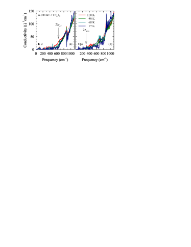
At the metal-insulator phase transition, we see an abrupt opening of an optical gap, with the conductivity in the overdamped Drude region dropping down to very low values as shown in Fig. 3. In order to illustrate the low-temperature electronic behavior more clearly, we have fitted the vibrational features by Lorentz and Fano curves, and subtracted them from the measured spectra. The results for both polarizations are plotted in Fig. 4 for different temperatures. The drop of below 1000 cm-1 can be extrapolated linearly to obtain a gap value cm-1 for , corresponding to approximately 75 meV; it is basically identical for both polarizations.note3 It is worth of noting that while the conductivity for is indeed close to zero at frequencies below 600 cm-1, the conductivity for remains finite down to about 400 cm-1. Thus taking only the range up to 800 cm-1 into account, we can extract gap values of 600 and 400 cm-1 from the linear extrapolation, which corresponds rather well to the one extracted from the dc conductivity measurements (see Fig. 8).
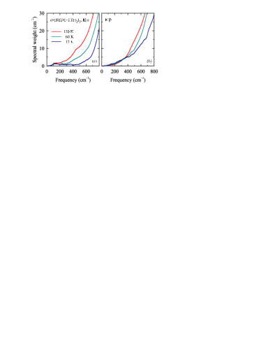
For spectral weight still moves from the gap region to higher frequencies as is reduced: it piles up around 1000 cm-1 and higher (Fig. 5). Interestingly, not only the region of the gap changes, but spectral weight in the entire range shifts to higher frequencies. The maximum of the mid-infrared band moves up slightly which in part can be described to thermal contraction, but mainly to the redistribution of spectral weight.
III.1.2 Vibrational features
Charge disproportionation.
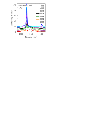
In order to characterize the redistribution of charge values on molecular sites associated with the charge ordering we followed the behavior of the infrared active charge-sensitive mode by measuring perpendicular to the conducting plane. This vibration is the out-of-phase contraction of the C=C double bonds in the BEDT-TTF rings which leads to a dipole-moment change parallel to the long axis of BEDT-TTF molecule. The frequency of this mode is sensitive to the charge population of the molecule and known to split upon passing through a charge-ordering phase transition.Moldenhauer93 ; Yamamoto05 In the metallic state () we observe a wide single band at about 1445 cm-1; the frequency corresponds to an average charge of per molecule. The charge diproportionation happens abruptly at K: in the CO insulating state the mode splits in two pairs of bands at 1415 and 1428 cm-1, and at 1500 and 1505 cm-1, as demonstrated in the waterfall plot of Fig. 6. The lower-frequency bands correspond to approximately and charge on the molecule, the upper-frequency modes to and . This charge redistribution remains constant on further cooling and is in agreement with the charges estimated by x-ray for the four different sites in the unit cell.Kakiuchi07 The comprehensive infrared and Raman experiments of Yue et al.Yue10 confirm our findings.
Coming back to the vibrational features; also for polarized parallel and , we observe changes in shape of some modes at the metal-insulator transition. Due to screening, no molecular vibrations can be seen above the metal-to-insulator phase transition. Below , the modes detected in the in-plane spectra are the features of totally symmetric vibrations of BEDT-TTF molecule emv coupled with electronic charge-transfer transitions which have been observed and assigned previouslyMeneghetti86 down to 300 cm-1. As a result of interaction with electronic transition they have a Fano-shape:Fano61 an anti-resonance at frequencies where they coincide with the electronic excitations and an asymmetric peaks shape when the electronic feature is separated in frequencies. Thus, for example the A feature and several symmetric and asymmetric CH3 vibrationsMeneghetti86 at about 1400 cm-1 not only shows a blue shift together with a charge-transfer band in the mid-infrared, but also changes shape to become a narrow and slightly asymmetric band (see Fig. 2). While the lower-frequency modes are only weakly seen for , in the insulating phase the spectra we observe (cf. Fig. 3) all of the Ag vibrations predicted by Meneghetti et al.:Meneghetti86 for instance, the mode at 260 cm-1 (associated with the deformation of the outer EDT rings), the mode at 124 cm-1 (associated with the deformation of the inner TTF rings). These bands are very intense only in the direction and barely seen in the polarization. This is in agreement with the symmetry breaking, i.e., both the intrinsic dimerisation along the stacks ( direction) and the stripes formed along the direction in the CO phase as depicted in Fig. 1(b). A more detailed discussion of the in-plane vibrational features was recently given by Yue et al. based on low-temperature transmission experiments.Yue10
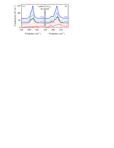
Interesting, that only the 410 cm-1 mode plotted in Fig. 7 changes on cooling in the insulating state. The band is much wider than the other features in this range at temperatures right below the metal-insulator transition and continuously narrows as is reduced. Following Meneghetti et al.Meneghetti86 we assign it to the mode which mainly involves the deformation of the outer rings.
Finally, the strong vibrational feature observed around 1300 cm-1 (not shown) is assigned to the emv coupled mode of the BEDT-TTF molecule. It is sharper and more pronounced for although the overall conductivity in the mid-infrared is about half compared to . Below 1000 cm-1 a large number of molecular and lattice vibrations peak out as soon as the screening by the conduction electrons is lost.
III.2 Transport
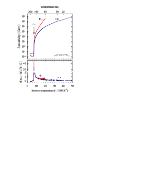
These measurements reveal that the small dc resistivity anisotropy known to be present at room temperature,Bender84-108 , pertains to the whole metallic regime and is approximately constant down to . As a new result it has to be pointed out that below the anisotropy of resistivity, hence also of conductivity, changes significantly with lowering temperature as the resistivity along the -axis rises more steeply than along the -axis, and at 50 K reaches (see Fig. 8). In our samples, despite temperature-dependent activation, the anisotropic transport gap in the CO phase for and can be estimated to about meV and 40 meV, respectively. At a first glance the appearance of an anisotropic transport gap seems to be at odds with the isotropic optical gap extracted from our optical measurements (Fig. 4). It is well known that systems with a complex band structure such as -(BEDT-TTF)2I3 may exhibit quite different optical and transport gaps: optical measurements examines direct transitions between the valence and conduction band, while dc transport probes transitions with the smallest energy difference between the two bands.
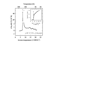
We have also characterized dc resistivity of -(BEDT-TTF)2I3 in the conducting plane, for , i.e., at an angle of approximately to the crystallographic axes. Metallic behavior of resistivity is present from room temperature down to 156 K. A sharp metal-to-insulator transition is confirmedDressel94 at K, which is apparent in the peak in with full width at half-height K; (Fig. 9). Below the transition the resistivity curve rises with a temperature-dependent activation indicating that a temperature-dependent conductivity gap opens of about 80 meV. No significant hysteresis in dc resistivity in the vicinity of could be found.
III.3 Dielectric Response
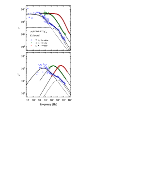
Low-frequency dielectric spectroscopy measurements were performed at various temperatures in the semiconducting phase. Representative spectra for are shown in Fig. 10. Most notably, between 35 K and up to 75 K two dielectric relaxation modes are discerned. The complex dielectric spectra can be described by the sum of two generalized Debye functions
| (1) |
where is the high-frequency dielectric constant, is the dielectric strength, the mean relaxation time and the symmetric broadening of the relaxation time distribution function of the large (LD) and small (SD) dielectric mode. The broadening parameter of both modes is typically . The temperature dependences of dielectric strengths and mean relaxation times are shown in Fig. 11. The dielectric strength of both modes does not change significantly with temperature (, ). At approximately 75 K the large dielectric mode overlaps the small mode. It is not clear whether the small dielectric mode disappears at this temperature or is merely obscured by the large dielectric mode due to its relative size. However, above 100 K, when the large dielectric mode shifts to sufficiently high frequencies, there are no indications of a smaller mode centered in the range – Hz. Accordingly, above 75 K fits to only a single Debye function are performed that we identify with the continuation of the large dielectric mode. All parameters of the large mode – such as dielectric strength, mean relaxation time, symmetric broadening of the relaxation time distribution function – can be extracted in full detail until it exits our frequency window at approximately 130 K. At temperatures up to 135 K (just below K) we can determine only the dielectric relaxation strength by measuring the capacitance at 1 MHz.
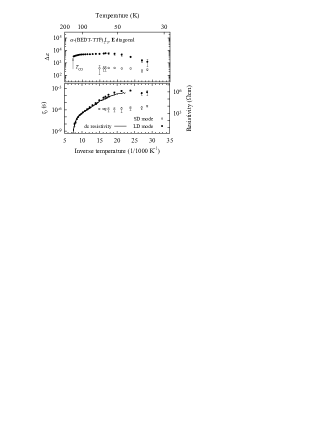
One of the most intriguing results is that the temperature behavior of the mean relaxation time differs greatly between the two dielectric modes. The large dielectric mode follows a thermally activated behavior similar to the dc resistivity, whereas the small dielectric mode is almost temperature-independent. This unexpected and novel behavior in the charge-ordered phase raised the possibility of anisotropic dielectric response. With this in mind we have performed another set of dc and ac spectroscopy measurements on the needle-shaped samples oriented along the - and -axis.
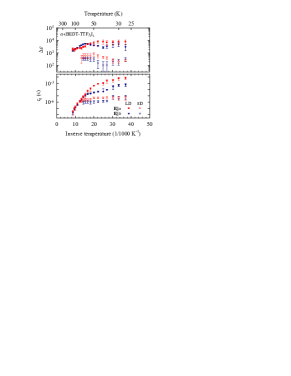
Low-frequency dielectric spectroscopy for both and orientation yields results comparable to : a large mode whose mean relaxation time follows dc resistivity, and a small, temperature-independent mode noticeable at temperatures below K. The fit parameters to model (1) are displayed in Fig. 12 as a function of inverse temperature. There is no prominent anisotropy or temperature dependence in dielectric strength, and the values of both the large and small dielectric modes correspond to those of the sample measured in diagonal orientation. However, an evolution of anisotropy in is clearly visible. Figure 14 shows that the newly-found anisotropy in closely follows the dc conductivity anisotropy.
IV Discussion
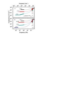
It is instructive to compare the conductivity of -(BEDT-TTF)2I3 as a function of temperature in the wide frequency range: from dc limit up to terahertz frequencies. Fig. 13 composes the conductivity spectra of -(BEDT-TTF)2I3 from dc, dielectric and optical measurements for and at different temperatures. First, we address the high-temperature phase. The Drude term in room-temperature spectra of organic conductors is known to be commonly very weak, if present at all.Dressel04 The optical conductivity of -(BEDT-TTF)2I3 is in accord to this observation, showing both along the - and -axes an overdamped Drude response at all temperatures above . The absence of a well-defined Drude peak in the vicinity of the CO transition resembles the behavior reported for the CO insulator -(BEDT-TTF)2RbZn(SCN)4.Wang01 Note that other -phase BEDT-TTF conductors, such as -(BEDT-TTF)Hg(SCN)4,Drichko06 do exhibit a zero-energy peak.
It is also worth of noting that the optical, dc resistivity and low-frequency dielectric measurements give mutually consistent values for the conductivity anisotropy at all temperatures above . The electronic part of optical spectra can be compared to calculations of the extended Hubbard model for a quarter-filled square lattice using Lanczos diagonalization. They predict a band with a maximum at approximately in the charge ordered insulating state,Merino03 which yields eV and eV for the respective directions. The values are in reasonable agreement with Hückel calculations performed by Mori et al.MoriCL84 and support the observed anisotropy in transport and optical properties.
Next we address the charge-order phase: how it develops on cooling, the ground state features and excitations observed by applied spectroscopic techniques. The vibrational spectra reveal that the static charge disproportionation sets in rather suddenly (Fig. 6) at the temperature of MI transition and is accompanied by the respective change in the optical properties of the conducting plane. At high temperatures, a wide single band at about 1445 cm-1 is observed whose frequency corresponds to an average charge of per molecule. According to Yue et al.Yue10 this band originates from slow fluctuations of the charge distribution at each site reflecting the partial charge ordering at short length scales as detected in NMR and x-ray measurements.Takahashi06 ; Kakiuchi07 Yue et al. estimate the site-charge distribution slightly above transition to be +0.6, +0.6 and , agreeing well with the x-ray data by Kakiuchi et al. The long-range charge diproportionation happens abruptly at K and remains constant on further cooling. In the CO insulating state the mode splits in two pairs of bands (see Fig. 6). The lower-frequency bands correspond to approximately and charge on the molecule, and the upper-frequency modes to and , which is in agreement with charge estimation by x-ray for the four different sites in the unit cell.Kakiuchi07
Interestingly though, optical gap and some of the features of outer ring BEDT-TTF vibrations show a continuous change on cooling in the CO state, indicating that some changes (but not a charge redistribution) happen with temperature in the insulating state. In contrast to the sharp onset of the vibration that monitors the static charge order and does not change below (see Fig. 6), we see some development of the gap and some of the emv coupled features on cooling in the charge-ordered state. In the region where the gap has opened (), the conductivity drops further and reaches zero only at the lowest measured temperature ( K). For instance, at K a finite conductivity is found all the way down to 200 cm-1 and even below, in accord with previous microwave measurements.Dressel94 ; Clauss09 The optical gap is more or less isotropic, in contrast to the pronounced anisotropy of the dc gap, which is explainable taking into account that different transitions are involved in optics and dc. Nevertheless, as mentioned in Section III, there is some weak indication that for excitations are possible to lower frequencies. The increase of the anisotropy at lower temperatures, which was observed in the dc limit, is not that clear in the optical data possibly due to strong phonon features and the low-conductivity base line. A similar dc conductivity anisotropy has been observed in the CO phase of (TMTTF)2AsF6.KorinHamzic06
In the charge-ordered phase we observe novel processes at lower frequencies, including CDW responses. As soon as the CO phase is entered, the low-frequency conductivity drops strongly leading to a step in the radio-frequency range (see Fig. 13). This corresponds to the broad and strongly temperature-dependent CDW relaxation mode (visible only below 120 K), which can be clearly seen in the spectra of imaginary part of dielectric function (Fig. 10). It is followed by a power law dispersion attributed to hopping transport (for more details on hopping conduction see Ref. VuleticPR, ), that leads to relatively high ac conductivity in the microwave and far-infrared region, as compared to the conductivity in dc limit (see Fig. 13). In the microwave region, the most prominent feature is the continuous increase of conductivity with rising frequency, while the far-infrared and infrared regions are mainly characterized by the suppression of the Drude weight, below either the CO gap and strong phonon features. Such behavior of conductivity is similar to the one observed for fully doped ladders in the (Sr,Ca)14Cu24O41 cuprates in which CDW is established. Conversely, comparable dc and optical conductivities were found in BaVS3 systems in which CDW is also observed.Kezsmarki06 In this way, we can classify the latter system as the fully ordered, while ladders and -(BEDT-TTF)2I3 show features known for disordered systems.
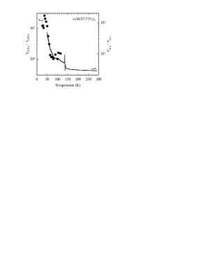
The observed ac conductivity data demonstrate a complex and anisotropic dispersion in the charge-ordered state. First, similar to the Peierls CDW state, we observe broad screened relaxation (large dielectric) modes along diagonal and both - and -axis of BEDT-TTF planes. These modes can be interpreted as signatures of long-wavelength charge excitations possessing an anisotropic phason-like dispersion. In -(BEDT-TTF)2I3 Kakiuchi et al. were the first to suggest a CDW which forms along the zig-zag path CABA′C of large overlap integrals detected in their x-ray diffraction measurements Kakiuchi07 . However, the presence of a modulation of overlap integrals along the - and -directions, ACA′BA and ABA′CA (see Fig. 15), hints at an additional complexity and makes the zig-zag paths a somewhat arbitrary choice. A theoretical model for the related quarter-filled -ET systems may provide a more appropriate scenario.Clay02 Clay et al. showed that the CO phase with horizontal stripe phase is characterized by a 1100 modulation of site charges along the two independent - and -directions parallel to the larger overlap integral, and with a 1010 modulation along the -axis perpendicular to the stripes. In addition, this CO is accompanied by a modulation, or tetramerization, of the overlap integrals along the -directions, the strongest overlap integral being 1-1 and the weakest 0-0. Further, a bond dimerization is also present along the molecular stacks. In other words, such a CO phase corresponds to a specific modulation of bonds and site charges, i.e., a combined bond-CDW along the two BEDT-TTF plane -directions with bond dimerization in stacking direction. As mentioned above, an analogous albeit more complex tetramerization of overlap integrals does develop along the -directions of -(BEDT-TTF)2I3. Using x-ray diffraction data, Kakiuchi et al. calculated overlap integrals between neighboring molecules based on the tight-binding approximation and a molecular orbital calculation with the extended Hückel method.Kakiuchi07 ; MoriBCSJ84 As shown in Fig. 15, along the -direction, ABA′CA, the strongest overlap integral is obtained between the two charge-rich sites A and B, quite alike the model bond order for the -material. Also, bond dimerization along the stacking -direction and its pattern in the plane of -(BEDT-TTF)2I3 agree with the model. However, in the -direction, ACA′BA, the order is shifted by one bond: the largest overlap integral is between the charge-rich A site and the charge-poor C site. Additionally, the overlap integrals are not perfectly sine-modulated along each -direction. While these deviations of -(BEDT-TTF)2I3 bond order from the -ET model should be recognized, they are hardly surprising. Indeed, -(BEDT-TTF)2I3 has a lower symmetry than a -structure which might induce slight differences in bond patterns. Also, the overlap integrals obtained from x-ray diffraction could somewhat depend on the employed method of calculation. This leaves the main physical result of the model by Clay et al., formation of a bond-CDW within the conducting molecular planes, fully applicable and relevant to the case of -(BEDT-TTF)2I3. It is plausible to look for the origin of phason-like dielectric relaxation in such a bond-CDW. In this case the energy scale of barrier heights is close to the single-particle activation energy indicating that screening by single carriers responsible for the dc transport is effective for this relaxation. The fact that the temperature behavior of the anisotropy closely follows the dc conductivity anisotropy has important implications: while the CDW motion is responsible for the dielectric response, the single electron/hole motion along the two -directions, possibly zig-zagging between them, is responsible for the observed dc charge transport.
The observation of a Peierls-like broad screened dielectric relaxation in 2D represents an important experimental result which clearly indicates that the charge order in -(BEDT-TTF)2I3 cannot be considered of fully localized Wigner type as predicted by a number of theoretical models.Kino9596 ; Seo06 Rather, as we have argued above, the bond-CDW delocalized picture appears as the most appropriate one. It is noteworthy that a similar 2D dispersion was previously observed in the CDW phase developed in the ladder layers of Sr14Cu24O41.VuleticPRL ; Vuletic05 ; Abbamonte04 Calculations based on the extended Hubbard model and the - model predicted sinusoidal charge-density modulation either of or type for this system.Dagotto92 ; Orignac97 ; White02 This result was at first met with surprise due to the strongly correlated nature of the ladders system. Nevertheless, the prediction was confirmed by resonant x-ray diffraction measurementsAbbamonte04 which indicated that the established CO is not of fully localized Wigner type, but that it can be described as a sinusoidal, delocalized modulation.

Further, we comment on the small dielectric mode whose features are characteristic of short-wavelength charge excitations. We suggest that the origin of this relaxation might be in the twinned nature of the CO phase due to the inversion symmetry breaking, with one domain being (A,B)-rich and the other (A′,B)-rich.Kakiuchi07 Indeed, a ferroelectric-like character to the charge-ordered phase is suggested by bond-charge dimerization along the -axis together with optical second-harmonic generation and photoinduced CO melting.Yamamoto08 ; Tanaka10 ; Nakaya10 Our data can be most naturally attributed to the motion of charged kink-type defects – solitons or domain walls in the charge order texture. Both domain walls and solitons stand for short wavelength excitations; however whereas a soliton is usually a one-dimensional object, the domain wall is not dimensionally restricted. Charge neutrality constraint of the CO in -(BEDT-TTF)2I3 (a change of stripes equivalent to strictly replacing unit cells of one twin type with another) suggests two types of solitons and/or domain walls. The first one is the domain wall in pairs (a soliton-antisoliton pair) between CR and CP stripes along the -axis, which we get if we impose the constraint along the -axis [Fig. 16(a)]. The second type of domain-wall pair is given by applying the constraint along the -axis so that the domain walls’ interior contains both charge signs [Fig. 16(b)]. The motion of such entities induces a displacement current and can therefore be considered as the microscopic origin of polarization in the CO state. Namely, in the presence of an external electric field perpendicular to the horizontal stripes, , coupling to the AA′ dipole moments of each unit cell breaks the symmetry between the two orientations of the dipole. Due to first-neighbor interactions the AA′ dipoles can most easily be flipped at the domain wall, causing the wall pairs to move. Coupling to a field in the configuration, parallel to stripe direction and therefore perpendicular to the AA′ dipoles, seems to be more troublesome. However, one only needs to remember that A and A′ also interact with B and C sites. At the energetically unfavorable domain wall the B and C molecules effectively couple AA′ dipoles to perpendicular external fields and allow for solitonic motion along the -axis as well.
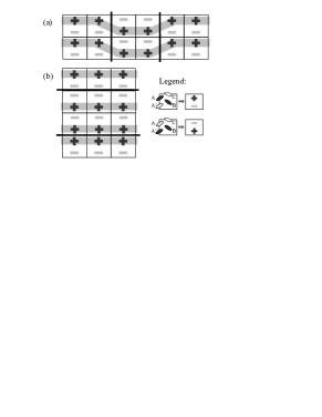
Theoretically, a domain wall should be independent on position, however in a real crystal it gets pinned to defect sites.Chaikinbook Such a pinning causes the domain wall to sit in a local energy minimum. The broad distribution of relaxation times might then be ascribed to a distribution of activation energies associated with pinning sites. A weak ac electric field induces a dielectric response which can be attributed to the activation between different metastable states over energies barriers. These metastable states correspond to local changes of charge distribution across the length scale of domain wall thickness. Finally, a nearly temperature-independent mean relaxation time indicates that resistive dissipation cannot be dominant for domain wall pairs and that the dielectric relaxation is governed by low energy barriers.
At the end, we consider alternative microscopic descriptions of excitations which could give rise to the dielectric relaxation in -(BEDT-TTF)2I3. A model proposed by Hotta et al.Hotta08 describes single-particle excitations in an insulating, horizontally-striped charge order on a triangular lattice using plaquette processes. These correspond to a localized charged particle moving between charge-rich and charge-poor stripes. However, the model does not lend itself easily to workable predictions of transport, dielectric and infrared properties. Another single-particle description might be found in the excitonic model used by Yamaguchi et al. to explain dielectric properties below K as well as nonlinear conductivity of -BEDT-TTFZn(SCN)4 (.Takahide06 ; Takahide10 This model considers a charge-ordered quarter-filled square-lattice system in which excitations are created by moving a localized hole to a site where no hole was originally present, thus creating a pair of a localized electron and hole. Due to their electric fields being confined to the polarizable plane of ET molecules, the attractive Coulomb potential between a bound electron and hole is of a logarithmic form: the potential is modeled as for , and a constant for , where the spatial scale is the distance between neighboring BEDT-TTF sites, nm, and is the screening length. At finite temperatures bound pairs are thermally excited. The potential barrier for a pair to unbind under an electric field is given by , . In the excitonic picture a transport gap naturally follows from the cutoff of logarithmic potential.Takahide10 The thermally excited but bound pairs are polarized in the presence of an electric field and give rise to a temperature-dependent dielectric constant
| (2) |
where is the electron-hole density at which we take to be equal to half the BEDT-TTF density.Takahide10 The above expression can be compared with the measured dielectric properties of -(BEDT-TTF)2I3. Namely, the total dielectric constant [] is well-approximated by the of LD mode (see Figs. 11 and 12). A two-parameter (, ) fit to, e.g., our data above K reproduces adequately the general temperature dependence, but gives a rather small nm and meV. The fit value of is in stark contrast with the value extracted from transport gap, meV (further, substituting from the previous expression gives an unsatisfactory one-parameter fit). A similar discrepancy can be seen in and fits. Also, it is not clear whether this model (here shown only in the static limit) reproduces the shapes of our experimental dielectric spectra and their temperature dependence. In the end the excitonic picture, while nicely applicable to -BEDT-TTFZn(SCN)4 below 2 K, does not seem to account for general dielectric features of -(BEDT-TTF)2I3 in the charge-ordered phase.
V Summary
We investigated electrodynamic properties in the single-crystals of the layered organic compound -(BEDT-TTF)2I3. In the normal phase, we observe an overdamped Drude response and a weak optical conductivity anisotropy. This is consistent with an almost isotropic, weakly temperature-dependent dc conductivity inside the conducting layers. Broad intramolecular vibrations of the BEDT-TTF molecule might be attributed to charge ordering fluctuations which form at short length scales. We demonstrate the abrupt onset of static charge order below K followed by a dramatic drop of the optical conductivity. The charge diproportionation remains constant on further cooling. The observed charge values are +0.8 and on charge-rich sites, and +0.2 and on charge-poor sites, consistent with the charges estimated by x-ray. Below the charge-order transition we detect the strong development of in-plane dc conductivity and dc gap anisotropy in contrast to the anisotropy of optical conductivity which remains weak and similar to high temperatures. The optical gap is approximately 75 meV. The development of dc conductivity anisotropy in the conducting layers is accompanied by appearance of two dielectric relaxation modes in kHz–MHz frequency range. The large dielectric mode features an anisotropic phason-like behavior, whereas the small dielectric mode is temperature-independent and its properties are reminiscent of a soliton-like behavior. All these results make it rather clear that the most consistent picture of the horizontal stripe, charge-ordered state in layered -(BEDT-TTF)2I3 is a cooperative bond-charge density wave with ferroelectric-like nature, rather than a fully localized Wigner-crystal. Additional theoretical and experimental work is warranted in order to refine the microscopic description of both metallic and insulating phase of -(BEDT-TTF)2I3. The emerging broader issue of the anisotropic, screened phason-like dispersion, its associated sinusoidal charge-density modulation and whether they are a general signature of charge order in layered strongly correlated systems certainly deserves further efforts.
Acknowledgements.
We thank G. Untereiner for the sample preparation and T. Vuletić for his help in data analysis. In addition, we wish to acknowledge the contribution of B. Gorshunov to the experimental part of this study. N.D. is grateful for the support by the Magarete-von-Wrangell-Programm of Baden-Württemberg. This work was supported by the Croatian Ministry of Science, Education and Sports under Grants No. 035-0000000-2836 and 035-0352843-2844 and by the Deutsche Forschungsgemeinschaft (DFG) under Grant DR 228/29-1. We also express our thanks to S. Mazumdar, T. Yamaguchi, C. Hotta, and S. Brown for enlightening discussions.References
- (1) P. Fulde, Electron Correlations in Molecules and Solids, 3rd edition, Springer-Verlag, Berlin (1995).
- (2) Molecular Conductors, Thematic Issue, Chemical Reviews 104, No. 11, November 2004.
- (3) G. Grüner, Rev. Mod. Phys. 60, 1129 (1988) and 66, 1 (1994).
- (4) P. B. Littlewood, Phys. Rev. B 36, 3108 (1987).
- (5) R. J. Cava, R. M. Fleming, R. G. Dunn, and E. A. Rietman, Phys. Rev. B 31, 8325 (1985).
- (6) T. Vuletić, B. Korin-Hamzić, T. Ivek, S. Tomić, B. Gorshunov, M. Dressel, and J. Akimitsu, Phys. Rep. 428, 169 (2006).
- (7) M. Dressel, N. Drichko, and S. Kaiser, Physica C 470, S589 (2010).
- (8) P. Monceau, F. Y. Nad, S. Brazovskii, Phys. Rev. Lett. 86, 4080 (2001).
- (9) K. Kanoda, J. Phys. Soc. Jpn. 75, 051007 (2006).
- (10) T. Takahashi, Y. Nogami, and K. Yakushi, J. Phys. Soc. Jpn. 75, 051008 (2006).
- (11) H. Seo, J. Merino, H. Yoshioka, and M. Ogata, J. Phys. Soc. Jpn. 75, 051009 (2006).
- (12) R. T. Clay, S. Mazumdar, and D. K. Campbell, J. Phys. Soc. Jpn. 71, 1816 (2002).
- (13) K. Bender, I. Hennig, D. Schweitzer, K. Dietz, H. Endres, and H. J. Keller, Mol. Cryst. Liq. Cryst. 108, 359 (1984).
- (14) N. Tajima, A. Ebina-Tajima, M. Tamura, Y. Nishio, and K. Kajita, J. Phys. Soc. Jpn. 71, 1832 (2002).
- (15) N. Tajima, J. Fujisawa, N. Naka, T. Ishihara, R. Kato, Y. Nishio, and K. Kajita, J. Phys. Soc. Jpn. 74, 511 (2005).
- (16) S. Iwai, K. Yamamoto, A. Kashiwazaki, F. Hiramatsu, H. Nakaya, Y. Kawakami, K. Yakushi, H. Okamoto, H. Mori, and Y. Nishio, Phys. Rev. Let.. 98, 097402 (2007).
- (17) K. Yamamoto, S. Iwai, S. Boyko, A. Kashiwazaki, F. Hiramatsu, C. Okabe, N. Nishi, and K. Yakushi, J. Phys. Soc. Jpn. 77, 074709 (2008).
- (18) T. Mori, J. Phys. Soc. Jpn. 79, 014703 (2010).
- (19) N. Tajima, S. Sugawara, M. Tamura, R. Kato, Y. Nishio, and K. Kajita, Eur. Phys. Lett. 80, 47002 (2007).
- (20) N. Tajima, S. Sugawara, R. Kato, Y. Nishio, and K. Kajita, Phys. Rev. Lett. 102, 176403 (2009).
- (21) Y. Kawakami, T. Fukatsu, Y. Sakurai, H. Unno, H. Itoh, S. Iwai, T. Sasaki, K. Yamamoto, K. Yakushi, and K. Yonemitsu, Phys. Rev. Lett. 105, 246402 (2010).
- (22) K. Bender, K. Dietz, H. Endres, H. W. Helberg, I. Hennig, H. J. Keller, H. W. Schäfer, and D. Schweitzer, Mol. Cryst. Liq. Cryst. 107, 45 (1984).
- (23) T. Mori, A. Kobayashi, Y. Sasaki, H. Kobayashi, G. Saito, and H. Inokuchi, Chem. Lett. 1984, 957 (1984).
- (24) S. Moroto, K.-I. Hiraki, Y. Takano, Y. Kubo, T. Takahashi, H. M. Yamamoto, T. Nakamura, J. Phys. IV (France) 114, 339 (2004).
- (25) Y. Takano, K. Hiraki, H. M. Yamamoto, T. Nakamura, and T. Takahashi, J. Phys. Chem. Solids 62, 393 (2001).
- (26) T. Kakiuchi, Y. Wakabayashi, H. Sawa, T. Takahashi, and T. Nakamura, J. Phys. Soc. Jpn. 76, 113702 (2007).
- (27) J. Moldenhauer, C. Horn, K. I. Pokhodnia, D. Schweitzer, I. Heinen, and H. J. Keller, Synth. Met. 60, 31 (1993).
- (28) M. Dressel and N. Drichko, Chem. Rev. 104, 5689 (2004).
- (29) N. Drichko, S. Kaiser, Y. Sun, C. Clauss, M. Dressel, H. Mori, J. Schlueter, E. I. Zhyliaeva, S. A. Torunova, and R. N. Lyubovskaya, Physica B 404, 490 (2009).
- (30) R. Wojciechowski, K. Yamamoto, K. Yakushi, M. Inokuchi, and A. Kawamoto, Phys. Rev. B 67, 224105 (2003).
- (31) M. Dressel, G. Grüner, J. P. Pouget, A. Breining, and D. Schweitzer, J. de Physique I (France) 4, 579 (1994); Synth. Met. 70, 929 (1995).
- (32) K. Tamura, T. Ozawa, Y. Bando, T. Kawamoto, and T. Mori, J. Appl. Phys. 107, 103716 (2010).
- (33) Y. Yue, K. Yamamoto, M. Uruichi, C. Nakano, K. Yakushi, S. Yamada, T. Hiejima, and A. Kawamoto, Phys. Rev. B 82, 075134 (2010).
- (34) T. Ivek, B. Korin-Hamzić, O. Milat, S. Tomić, C. Clauss, N. Drichko, D. Schweitzer, and M. Dressel, Phys. Rev. Lett. 104, 206406 (2010).
- (35) http://www.ccp14.ac.uk/tutorial/lmgp/orientexpress.htm
- (36) P. Lunkenheimer, V. Bobnar, A. V. Pronin, A. I. Ritus, A. A. Volkov, and A. Loidl, Phys. Rev. B 66, 052105 (2002).
- (37) V. Želzný, J. Petzelt, R. Swietlik, B. P. Gorshunov, A. A. Volkov, G. V. Kozlov, D. Schweitzer, and H. J. Keller, J. Phys. I (France) 51, 869 (1990).
- (38) T. Sugano, K. Yamada, G. Saito, and M. Kinoshita, Solid State Commun. 55, 137 (1985).
- (39) M. Meneghetti, R. Bozio, and C. Pecile, J. Physique 47, 1377 (1986); Synth. Met. 19, 143 (1987).
- (40) K. Yakushi, H. Kanbara, H. Tajima, H. Kuroda, G. Saito, and T. Mori, J. Phys. Soc. Jpn 60, 4251 (1987).
- (41) R. Zamboni, D. Schweitzer, H. J. Keller, and C. Taliani, Z. Naturforsch. 44a, 295 (1989).
- (42) S. Gärtner, D. Schweitzer, and H. J. Keller, Synth. Met. 44, 227 (1991).
- (43) C. Clauss, N. Drichko, D. Schweitzer, and M. Dressel, Physica B 405, 144 (2010).
- (44) T. Yamamoto, M. Uruichi, K. Yamamoto, K. Yakushi, A. Kawamoto, and H. Taniguchi, J. Phys. Chem. B 109, 15226 (2005).
- (45) N. L. Wang, H. Mori, S. Tanaka, J. Dong, and B. P. Clayman, J. Phys.: Cond. Matter 13, 5463 (2001).
- (46) N. Drichko, M. Dressel, C. A. Kuntscher, A. Pashkin, A. Greco, J. Merino, and J. Schlueter, Phys. Rev. B 74, 235121 (2006); M. Dressel, N. Drichko, J. Schlueter, and J. Merino, Phys. Rev. Lett. 90, 167002 (2003).
- (47) The maxima in optical conductivity are obscured by the antiresonance at these frequencies, leaving only two side peaks remaining.
- (48) J. Merino, A. Greco, R. H. McKenzie, and M. Calandra, Phys. Rev. B 68 245121 (2003).
- (49) The difference to Ref. Dressel94, (where cm is given) is mainly due to the way how the gap value was determined.
- (50) I. Kézsmárki, G. Mihály, R. Gaal, N. Barišić, A. Akrap, H. Berger, L. Forró, C. C. Homes, and L. Mihály, Phys. Rev. Lett. 96, 186402 (2006).
- (51) U. Fano, Phys. Rev. 124, 1866 (1961).
- (52) B. Korin-Hamzić, E. Tafra, M. Basletić, A. Hamzić, and M. Dressel, Phys. Rev. B 73, 115102 (2006).
- (53) H. Kino and H. Fukuyama, J. Phys. Soc. Jpn. 64, 4523 (1995); 65, 2158 (1996).
- (54) T. Vuletić, B. Korin-Hamzić, S. Tomić, B. Gorshunov, P. Haas, T. Rôôm, M. Dressel, J. Akimitsu, T. Sasaki, and T. Nagata, Phys. Rev. Lett 90, 257002 (2003).
- (55) T. Vuletić, T. Ivek, B. Korin-Hamzić, S. Tomić, B. Gorshunov, P. Haas, M. Dressel, J. Akimitsu, T. Sasaki, and T. Nagata, Phys. Rev. B 71, 012508 (2005).
- (56) P. Abbamonte, G. Blumberg, A. Rusydi, A. Gozar, P. G. Evans, T. Siegrist, L. Venema, H. Eisaki, E. D. Isaacs, and G. A. Sawatzky, Nature 431 1078 (2004).
- (57) E. Dagotto, J. Riera, and D. Scalapino, Phys. Rev. B 45, 5744 (1992).
- (58) E. Orignac and T. Giamarchi, Phys. Rev. B 56, 7167 (1997).
- (59) S. R. White, I. Affleck, and D. J. Scalapino, Phys. Rev. B 65, 165122 (2002).
- (60) T. Mori, A. Kobayashi, Y. Sasaki, H. Kobayashi, G. Saito, and H. Inokuchi, Bull. Chem. Soc. Jpn. 57, 627 (1984).
- (61) Y. Tanaka and K. Yonemitsu, J. Phys. Soc. Jpn. 79, 024712 (2010).
- (62) H. Nakaya, K. Itoh, Y. Takahashi, H. Itoh, S. Iwai, S. Saito, K. Yamamoto, and K. Yakushi, Phys. Rev. B 81, 155111 (2010).
- (63) P. M. Chaikin and T. C. Lubensky, Principles of Condensed Matter Physics (Cambridge University Press, Cambridge, 1995), Sec. 10.
- (64) C. Hotta and F. Pollmann, Phys. Rev. Lett. 100, 186404 (2008).
- (65) Y. Takahide, T. Konoike, K. Enomoto, M. Nishimura, T. Terashima, S. Uji, and H. M. Yamamoto, Phys. Rev. Lett. 96, 136602 (2006).
- (66) Y. Takahide, M. Kimata, K. Hazama, T. Terashima, S. Uji, T. Konoike, and H. M. Yamamoto, Phys. Rev. B 81, 235110 (2010).