Polychromatic nanofocusing of surface plasmon polaritons
Abstract
We introduce the concept of polychromatic plasmonics and suggest an broadband plasmonic lens for nanofocusing of surface plasmon polaritons. The lens employs a parabolically modulated metal-dielectric-metal structure. This plasmonic lens has a bandwidth of more than an optical octave thus opening new opportunities for broadband plasmonic applications.
pacs:
78.67.-n, 78.67.Pt, 42.25.BsThe field of plasmonics experiences an explosive growth recently due to the ability of plasmonic components to confine light down to the nanoscale. Various plasmonic structures with miniaturization scales comparable to those of modern semiconductor electronics have been designed to realize different types of light waveguiding and control Cao and Brongersma (2009); Zayats et al. (2005); Gramotnev and Bozhevolnyi (2010); Lee et al. (2010); Liu et al. (2010); Huidobro et al. (2010); Verslegers et al. (2009). Despite the boom in research one can identify two major challenges for further applications of plasmonic devices: high propagation loss and strong wavelength dispersion. Different approaches to combat optical losses in metals have been explored, including incorporation of gain Noginov et al. (2008) or nanofocusing Stockman (2004); Davoyan et al. (2010). However, the concept of broadband control and nanofocusing of polychromatic surface plasmon polaritons (SPPs) remains practically unattainable.
In this Letter, we introduce the concept of polychromatic plasmonics and demonstrate the functionalities of a broadband plasmonic lens based on a metal-dielectric-metal (MDM) structure (Fig. 1). We utilize quadratic modulation of the thickness of the dielectric layer in transverse direction [Fig. 1(b)] to produce a parabolic optical potential which is practically wavelength independent. We develop analytical descriptions and employ numerical simulations to show its capability of three-dimensional subwavelength manipulations, including nanofocusing, self-collimation, and optical pendulum effect. The nanofocusing of our lens is demonstrated over a bandwidth exceeding an optical octave ( nm) thus allowing for polychromatic plasmon focusing.
The concept of polychromatic light propagation is well developed for dielectric structures, of which the polychromatic dynamic localization is a noticeable example Szameit et al. (2009). In these structures, curved waveguides are employed to produce an effective wavelength invariant optical potential to compensate for the dispersion.
In plasmonics, the engineering of the optical potentials for SPPs has been a key concept for designing plasmonic lenses and other elements Vedantam et al. (2009); Liu et al. (2010); Huidobro et al. (2010). Two kinds of structures with transverse Verslegers et al. (2009); Lee et al. (2010) or longitudinally varied effective index Stockman (2004); Durach et al. (2007) are mainly used. In the structures with transverse index modulation the plasmonic potentials are usually heavily wavelength dependent Lee et al. (2010); Liu et al. (2010); Huidobro et al. (2010); Verslegers et al. (2009). On the other hand, in longitudinally modulated structures light of different wavelengths can be focused asymptotically Durach et al. (2007) in the same taper, however light is fully localized there and could not propagate beyond the focus point Stockman (2004); Durach et al. (2007). Recently a variation of a plasmonic lens was shown to focus broadband light based on diffraction Gao et al. (2010). However, the focusing was obtained for light in free space rather than for propagating SPPs, thus with low focusing resolution. The focusing of polychromatic SPPs still remains an unsolved challenge.
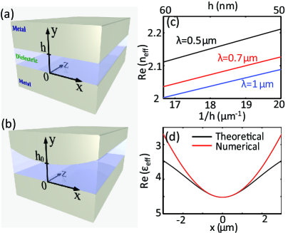
To address this challenge, first we consider a flat MDM waveguide shown in Fig. 1(a). We only consider the symmetric modes of the structure (with respect to the magnetic field distribution) because it is primarily excited by simple end-fire coupling, while the antisymmetric mode experiences a cut-off for the parameters of our work Zayats et al. (2005). The dielectric is chosen to be silica glass with permittivity , and the metal is silver for which we use the Drude model, , where , , are the angular frequency, plasma frequency and collision frequency, respectively. This model is proven to be a good approximation for noble metals, including silver in the spectral range above 500 nm. For silver we take rad/s and . Fig. 1(c) shows the real part of the mode index, , versus the inverse thickness of the dielectric for three different wavelengths. The dependence is linear, consistent with the theoretical approximation Bozhevolnyi and Jung (2008); Bozhevolnyi and Nerkararyan (2009),
| (1) |
where both and are complex parameters and could be extracted from data fitting. Most importantly, the slope of these curves is practically wavelength independent which allows for the design of broadband optical potential and polychromatic plasmon propagation.
Using the effective refractive index in Eq. (1), it is possible to construct a parabolic optical potential Arnaud (1976) for SPPs. This is achieved by a MDM waveguide with one flat and one parabolically curved surfaces as shown in Fig. 1(b). The thickness of the dielectric is , with as an effective radius (). In this waveguide, we obtain a parabolic optical potential under the condition of :
| (2) |
where , and is the focusing strength. Fig. 1(d) shows the results calculated by Eq. (2) and numerically for nm, m, and m.
Using the effective index method for the structure shown in Fig. 1(b), we can express the vertical electric field as Bozhevolnyi (2006); Bozhevolnyi and Nerkararyan (2009). When , and could be decoupled Bozhevolnyi and Nerkararyan (2009). The expression for could be found in Refs. Zayats et al. (2005); Bozhevolnyi and Nerkararyan (2009), while the equation for is Arnaud (1976); Marcuse (1972)
| (3) |
where and , . This is a harmonic oscillator equation with eigenmodes Arnaud (1976); Marcuse (1972), where is the characteristic width of the plasmonic waveguide, is the Hermite polynomial and the effective indices of different modes, under the paraxial approximation, are .
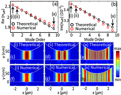
We also calculate the eigenmodes of this structure using commercial Mode Solutions (MS) software (Lumerical) with the parameters m, m, m, nm and m. The results of our analytical theory [Eq. (3)] and the MS calculations are summarized in Fig. 2. Fig. 2(a,b) shows the real and imaginary parts of for different modes with the theoretical field distribution of [Fig. 2(c-e)] and numerically calculated total field [Fig. 2(f-h)], which show a good agreement for low order modes. For higher order modes, larger discrepancy appears in terms of both effective index and field distribution. This is consistent with the results in Fig. 1(d), as the higher order modes spread out to the larger values, where the assumption does not strictly hold and the potential is not exactly parabolic.
Next we study the SPPs propagation in the structure. An incident beam could excite modes of different orders, which will then interfere with one another, producing different intensity patterns inside the structure. As a result of this interference, a range of SPPs beam manipulations is possible, including focusing, self-collimation, and optical pendulum effect Arnaud (1976); Marcuse (1972).
When can be decoupled from and changes slowly with , the input beam expansions along and inside the structure are independent. Considering that the beam distribution along can be fully characterized by , we study only the beam dynamics in the plane. The beam could be expanded into a complete set of orthogonal modes Marcuse (1972) , where is the expansion coefficient of the -order mode. If the initial beam has a Gaussian distribution , where is the beam width, the beam inside the structure, under paraxial approximation, is Arnaud (1976); Marcuse (1972):
| (6) |
where , , and . In the lossless case with , the beam intensity can be expressed as: with dynamic beam width varying along propagation:
| (7) |
The plasmon polariton beam is thus oscillating periodically along . It is easy to prove that the maximum and minimum dynamic beam widths are constrained by Arnaud (1976) , indicating that the beam is trapped in the parabolic optical potential.
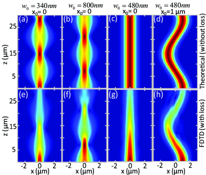
To confirm our theoretical analysis, we preform finite-difference-time domain (FDTD) simulations (Lumerical). All initial beams are -polarized with transverse Gaussian distributions to guarantee the excitation of SPPs modes. The structure parameters are the same as in the MS simulation, with m and perfectly matched layers at the boundaries. The analytical results without loss and the numerical results with loss are presented in Fig. 3. The data are shown for the plane in the middle of the gap, nm.
For an on-axis input beam () [Fig. 3(a, b, e, f)], one can observe periodic beam focusing with a period of
| (8) |
The points of maximum intensity correspond to the focusing when all excited modes interfere constructively. There is an initial phase shift depending on the ratio of the incident beam width and the characteristic width of the plasmonic waveguide . When these two widths match , one can observe self-collimation effect - diffractionless propagation of the beam [see Fig. 3(c, g)]. For an off-axis input beam () there are transverse oscillations [see Fig. 3(d, h)], and the plasmon polariton beam propagation exhibits an analog of optical pendulum behavior in a parabolic potential. The comparison with FDTD results suggests that losses do not affect the beam propagation except for attenuation along direction.
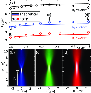
Eq. (8) has some important implications for propagation of polychromatic SPPs beams. As is practically wavelength independent while varies slowly [Fig. 1(c)], the focusing strengths and the oscillation period F are nearly the same for different wavelengths. For example, in Fig. 4(a) we show both the theoretical (solid line) and FDTD (circles) results for an input beam with for three different thicknesses in the wide wavelength range m. The different color beams focus at the planes of . The dispersionless characteristic of enables broadband SPPs focusing and distinguishes our plasmonic structure from other highly wavelength dependent structures Lee et al. (2010); Verslegers et al. (2009). In Fig. 4(b-d) we show the field distribution on the plane of nm for the three points marked in Fig. 4(a) at nm. False colors are used to indicate schematically the three different wavelengths. It is important to note that the focal planes of all spectral components coincide within 500 nm (less than one wavelength deviation in the spectral range m) and are practically indistinguishable. Note that the focal depth is in the range of m for the different spectral components. Fig. 4 proves that this structure acts as a lens for broadband polychromatic light focusing, a functionality that has never before been discussed in other plasmonic structures. From Fig. 4 and Eq. (8), it is clear that one can control the position of the focusing points by varying the thicknesses and/or the wire curvature , which enables wide reconfigurability of our structure.
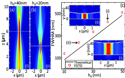
Finally, we investigate the focusing resolution of this structure, which is characterized by the full width at half maximum (FWHM) along direction at the focal plane. (Along the vertical direction the resolution can be approximately characterized by the thickness of the dielectric layer as shown in the insets of Fig. 5.) We define the wavelength of the SPPs, , which is smaller than the light wavelength in the dielectric, . What makes SPPs special is that its wavelength could be made as small as required, even vanishing for localized surface plasmons Zayats et al. (2005). In our lens-like structure, if we want to improve the focusing resolution, we could decrease . For a fixed vacuum wavelength, the simplest approach to increase is to make the thickness smaller. Fig. 5 shows the dependency of FWHM along at the focal plane for a fixed wavelength m and nm. Fig. 5(a, b) shows the field distribution along propagation for the two points marked in Fig. 5(c) in the plane of (20 nm and 10 nm, respectively). The white dashed lines indicate the focal planes. Insets (i) and (ii) show the transverse field distribution of at the two focusing planes. As shown in Fig. 5, the FWHM could be as small as 100 nm. This could be further improved by decreasing and/or increasing the focusing strength . Our results clearly show that the light is fully confined in the dielectric along and trapped in the optical parabolic potential along .
In conclusion, we have suggested the concept of polychromatic plasmonics and demonstrated a broadband plasmonic lens based on a parabolically modulated MDM structure. We have shown the plasmonic lens allows for complete three-dimensional subwavelength control of a beam, bringing a potential functionality for manipulation of ultra-short optical signals. The focusing capability of this plasmonic lens could be further improved by tapering the dielectric layer along the propagation direction Bozhevolnyi and Nerkararyan (2010). We anticipate the proposed structure is a promising candidate for broadband plasmonic applications including subwavelength white light imaging, polychromatic plasmon solitons, and ultrashort pulse plasmonic nanolasers. Furthermore, our ideas can be extended beyond the field of plasmonics, to include quantum particles in parabolic potentials, considering the similarity between Shrödinger equation and paraxial wave equation.
We thank A. A. Sukhorukov, Z. Xu, A. S. Desyatnikov, C. G. Poulton, and A. E. Minovich for useful discussions, and acknowledge a support from the Australian Research Council and the NCI Merit Allocation Scheme.
References
- Cao and Brongersma (2009) L. Cao and M. L. Brongersma, Nat. Photonics 3, 12 (2009).
- Zayats et al. (2005) A. V. Zayats, I. I. Smolyaninov, and A. A. Maradudin, Phys. Rep. 408, 131 (2005).
- Gramotnev and Bozhevolnyi (2010) D. K. Gramotnev and S. I. Bozhevolnyi, Nat. Photonics 4, 83 (2010).
- Lee et al. (2010) B. Lee, S. Kim, H. Kim, and Y. Lim, Prog. Quantum Electron. 34, 47 (2010).
- Liu et al. (2010) Y. M. Liu, T. Zentgraf, G. Bartal, and X. Zhang, Nano Lett. 10, 1991 (2010).
- Huidobro et al. (2010) P. A. Huidobro, M. L. Nesterov, L. Martin-Moreno, and F. J. Garcia-Vidal, Nano Lett. 10, 1985 (2010).
- Verslegers et al. (2009) L. Verslegers, P. B. Catrysse, Z. F. Yu, and S. H. Fan, Phys. Rev. Lett. 103, 033902 (2009).
- Noginov et al. (2008) M. A. Noginov, G. Zhu, M. Mayy, B. A. Ritzo, N. Noginova, and V. A. Podolskiy, Phys. Rev. Lett. 101, 226806 (2008).
- Stockman (2004) M. I. Stockman, Phys. Rev. Lett. 93, 137404 (2004).
- Davoyan et al. (2010) A. R. Davoyan, I. V. Shadrivov, A. A. Zharov, D. K. Gramotnev, and Y. S. Kivshar, Phys. Rev. Lett. 105, 116804 (2010).
- Szameit et al. (2009) A. Szameit, I. L. Garanovich, M. Heinrich, A. A. Sukhorukov, F. Dreisow, T. Pertsch, S. Nolte, A. Tuennermann, and Y. S. Kivshar, Nat. Phys 5, 271 (2009).
- Vedantam et al. (2009) S. Vedantam, H. Lee, J. Tang, J. Conway, M. Staffaroni, and E. Yablonovitch, Nano Letters 9, 3447 (2009).
- Durach et al. (2007) M. Durach, A. Rusina, and M. I. Stockman, Nano Lett. 7, 3145 (2007).
- Gao et al. (2010) H. Gao, J. K. Hyun, M. H. Lee, J.-C. Yang, L. J. Lauhon, and T. W. Odom, Nano Lett. 10, 4111 (2010).
- Bozhevolnyi and Jung (2008) S. I. Bozhevolnyi and J. Jung, Opt. Express 16, 2676 (2008).
- Bozhevolnyi and Nerkararyan (2009) S. I. Bozhevolnyi and K. V. Nerkararyan, Opt. Express 17, 10327 (2009).
- Arnaud (1976) J. A. Arnaud, Beam and fiber optics (Academic Press, New York, 1976).
- Bozhevolnyi (2006) S. I. Bozhevolnyi, Opt. Express 14, 9467 (2006).
- Marcuse (1972) D. Marcuse, Light transmission optics (Van Nostrand Reinhold, New York, 1972).
- Bozhevolnyi and Nerkararyan (2010) S. I. Bozhevolnyi and K. V. Nerkararyan, Opt. Lett. 35, 541 (2010).