Robust Level Coincidences in the Subband Structure of Quasi 2D Systems
Abstract
Recently, level crossings in the energy bands of crystals have been identified as a key signature for topological phase transitions. Using realistic models we show that the parameter space controlling the occurrence of level coincidences in energy bands has a much richer structure than anticipated previously. In particular, we identify robust level coincidences that cannot be removed by a small perturbation of the Hamiltonian compatible with the crystal symmetry. Different topological phases that are insulating in the bulk are then separated by a gapless (metallic) phase. We consider HgTe/CdTe quantum wells as a specific example.
pacs:
71.20.-b, 73.21.Fg, 03.65.VfRecently level crossings in the energy bands of crystals have become a subject of significant interest as they represent a key signature for topological phase transitions induced, e.g., by tuning the composition of an alloy or the thickness of a quasi two-dimensional (2D) system kan05z ; mur07 ; has10 ; qi10z . For example, it was proposed ber06a and soon after confirmed experimentally koe07 ; rot09 that HgTe/CdTe quantum wells (QWs) show a phase transition from spin Hall insulator to a quantum spin Hall regime when the lowest electron-like and the highest hole-like subbands cross at a critical QW width of Å; see also mur07 ; koe08 ; liu08 ; dai08 ; luo10 . Here we present a systematic study of level crossings and anticrossings in the subband structure of quasi 2D systems. We show that the parameter space characterizing level crossings has a much richer structure than previously anticipated. In particular, we present examples for robust level coincidences that are preserved while the system parameters are varied within a finite range. Similar to the topological phase transitions characterizing the quantum Hall effect tho82 , the insulating topological phases kan05z thus get separated by a gapless (metallic) phase. Such an additional phase was previously predicted in Ref. mur07a . Yet it was found that this phase could occur only in 3D, but not in 2D. Also, it was not clear which systems would realize such a phase. Here we take HgTe/CdTe QWs as a realistic example, though many results are relevant also for other quasi 2D systems
Level crossings were studied already in the early days of quantum mechanics hun27 ; neu29a ; her37z . They occur, e.g., when atoms are placed in magnetic fields in the transition region between the weak-field Zeeman effect and the high-field Paschen-Back effect. Also, they occur when molecules and solids are formed from isolated atoms. Hund hun27 pointed out that adiabatic changes of 1D systems—unlike multi-dimensional systems—cannot give rise to level crossings. Von Neumann and Wigner neu29a quantified how many parameters need to be varied for a level crossing. While levels of different symmetries (i.e., levels transforming according to different irreducible representations, IRs) may cross when a single parameter is varied, to achieve a level crossing among two levels of the same symmetry, it is in general necessary to vary three (two) independent parameters if the underlying eigenvalue problem is Hermitian (orthogonal). Subsequently, this problem was revisited by Herring her37z who found that the analysis by von Neumann and Wigner was not easily transferable to energy bands in a crystal due to the symmetry of the crystal potential. Similar to energy levels in finite systems, levels may coincide in periodic crystals if the levels have different symmetries. Of course, unless the crystal is invariant under inversion, this can occur only for high-symmetry lines or planes in the Brillouin zone (BZ), where the group of the wave vector is different from the trivial group . If at one end point of a line of symmetry a band with symmetry is higher in energy than the band with symmetry , while at the other end point the order of and is reversed, these levels cross somewhere in between and . Herring classified a level crossing as “vanishingly improbable” if it disappeared upon an infinitesimal perturbation of the crystal potential compatible with all crystal symmetries. In that sense, a level coincidence at a high-symmetry point of the BZ such as the point becomes vanishingly improbable. For energy levels with the same symmetry, Herring derived several theorems characterizing the conditions under which level crossings may occur. In particular, he found that in the absence of inversion symmetry level crossings that are not vanishingly improbable may occur for isolated points such that these crossings cannot be destroyed by an infinitesimal change in the crystal potential, but they occur at some point near . Here we identify several examples for such robust level coincidences. This illustrates that level coincidences in energy bands can be qualitatively different from level coincidences in other systems neu29a .
Recently, several studies focusing on topological phase transitions recognized the importance of symmetry for level crossings in energy bands mur07 ; koe08 ; liu08 ; dai08 . Murakami et al. mur07 studied the phase transition separating spin Hall insulators from the quantum spin Hall regime, focusing on generic low-symmetry configurations with and without inversion symmetry. They found that without inversion symmetry the phase transition is accompanied by a gap closing at points that are not high-symmetry points. In inversion symmetric systems the gap closes only at points where is a reciprocal lattice vector. Here we show that level crossings in quasi 2D systems can be characterized by a multitude of scenarios, taking HgTe/CdTe quantum wells as a specific example for which it is known that the lowest electron-like and the highest hole-like subbands (anti)cross for a critical QW width of about Å ber06a ; koe07 ; rot09 ; pfe00 . In most semiconductors with a zinc blende structure (point group ) the -antibonding orbitals form the conduction band (IR of ), whereas the -bonding orbitals form the valence band ( and of ). The curvature of the band is thus positive whereas it is negative for the band. For finite , the fourfold degenerate states (effective spin ) split into so-called heavy hole (HH, ) and light hole (LH, ) branches. In HgTe, the order of the and bands is reversed: is located below and it has a negative (hole-like) curvature, whereas splits into an electron () and a hole () branch dor83z . HgTe and CdTe can be combined to form a ternary alloy HgxCd1-xTe, where the fundamental gap between the and bands can be tuned continuously from eV in CdTe to eV in HgTe with a gapless material for dor83z . Tuning the material composition thus allows one to overcome Herring’s conclusion her37z that a degeneracy at between two levels of different symmetries is, in general, vanishingly improbable.
Layers of HgTe and CdTe can also be grown epitaxially on top of each other to form QWs. At the interface the corresponding states need to be matched appropriately. The opposite signs of the effective mass inside and outside the well result in eigenstates localized at the interfaces lin85 . We calculate these eigenstates as well as the corresponding subband dispersion using a realistic multiband Hamiltonian for the bulk bands , , and , which fully takes into account important details of such as anisotropy, nonparabolicity, HH-LH coupling, and spin-orbit coupling both due to bulk inversion asymmetry (BIA) of the zinc blende structure of HgTe and CdTe as well as structure inversion asymmetry (SIA) of the confining potential . For details concerning and its numerical solution see Refs. win03 ; bia-coeffs . In the following denotes the 2D wave vector.
The symmetry group of a QW and thus the allowed level crossings depend on the crystallographic orientation of the surface used to grow a QW [a (001) surface being the most common in experiments]. It also depends on whether we have a system without or with BIA and/or SIA. The resulting point groups are summarized in Table 1. We show below that these different groups give rise to a rich parameter space for the occurrence of level coincidences. For a proper symmetry classification we project the eigenstates of onto the IRs of the respective point group bir74 . In the following, all IRs are labeled according to Koster et al. kos63 . As spin-orbit coupling plays a crucial role for BIA and SIA win03 as well as for topological phase transitions kan05z ; mur07 ; has10 ; qi10z , all IRs referred to in this work are double-group IRs. For comparison, Table 1 also lists the point groups if the prevalent axial (or spherical) approximation is used for . In this approximation, BIA is ignored and different surface orientations become indistinguishable.
| axial appr. | ||||||||
|---|---|---|---|---|---|---|---|---|
| sym. | ||||||||
| asym. | ||||||||
| sym. | ||||||||
| asym. |
First we neglect the small terms in due to BIA so that the bulk Hamiltonian has the point group . In the absence of SIA, a quasi 2D system grown on a (001) surface has the point group (which includes inversion) and all electron and hole states throughout the BZ are two-fold degenerate bir74 . Subband edges in a HgTe/CdTe QW as a function of well width are shown in Fig. 1(a). The HH states transform according to of . The electron-like and LH-like subbands transform according to . As expected, the and subbands may cross as a function of .
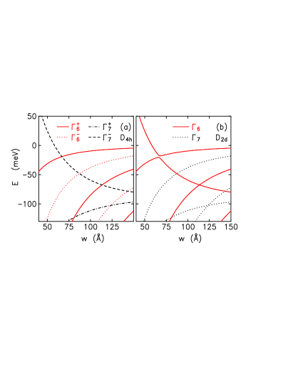
In the presence of SIA we cannot classify the eigenstates anymore according to their behavior under parity. Without BIA the point group becomes . HH states transform according to of and electron- and LH-like states transform according to . The level crossings depicted in Fig. 1(a) remain allowed in this case koe08 ; rot10 .
The situation changes when taking into account BIA. Without SIA the point group becomes . In this case, all subbands transform alternately according to the IRs and of , irrespective of the dominant spinor components. In particular, both the highest HH state and the lowest conduction band state transform according to of so that around Å we obtain an anticrossing between these levels of about meV (for ), see Fig. 1(b) koe08 ; liu08 ; dai08 . With both BIA and SIA the point group becomes . Now we have only one double group IR . Thus it follows readily that all subbands anticross as a function of a continuous parameter such as the well width.
While BIA opens a gap at , level coincidences remain possible for some when the well width is tuned to a critical value mur07 ; her37z . Considering a (001) surface with BIA, we find, indeed, that for each direction of , critical values and exist that give rise to a band crossing. Thus we get a line in space where the bands cross when is varied within some finite range. This result holds for QWs on a (001) surface with BIA, without and with SIA (as studied experimentally in Refs. koe07 ; rot09 ). As an example, Fig. 2(a) shows in the presence of a perpendicular electric field kV/cm.
In general, three independent parameters must be tuned for a level coincidence in a quantum mechanical systems neu29a if the underlying eigenvalue problem is Hermitian. While the multiband Hamiltonian used here win03 is likewise Hermitian (not orthogonal), only two independent parameters ( and ) are necessary to achieve the level degeneracy. We have here an example for the robustness of band coincidences under perturbations that was predicted by Herring her37z to occur in systems without a center of inversion (in multiples of four). It shows that level coincidences in energy bands can behave qualitatively different from level coincidences in other quantum mechanical systems neu29a . We note that the band coincidences found here are not protected by symmetry in the sense that—unlike the other cases discussed above—the group of is the trivial group containing only the identity.

The situation is different for quasi 2D systems grown on a (111) surface. In the absence of BIA and SIA, the point group is . HH states at transform according to the complex conjugate IRs or , where indicates that these IRs must be combined due to time reversal symmetry. All other subband edges transform according to . In the presence of BIA and/or SIA the point group becomes . Then HH states transform according to the complex conjugate IRs . Electron-like and LH-like states transform according to . Thus it follows that on a (111) surface the HH states always cross the other states at as a function of [similar to Fig. 1(a)]. The IRs for different geometries starting out from a (001) or (111) surface are summarized in Table 2.
| (001) | (111) | ||||||
|---|---|---|---|---|---|---|---|
| bulk | group | c, LH | HH | group | c, LH | HH | |
| sym. | |||||||
| asym. | |||||||
| sym. | |||||||
| asym. | |||||||
Finally we consider quasi 2D states on a (110) surface. In the absence of BIA and SIA, the point group becomes . Here, all subbands transform alternately according to and with the topmost HH-like subband being and the lowest electron-like subband being . A level crossing as a function of is thus again allowed at . In the presence of either BIA or SIA the symmetry is reduced to . While the point group in both cases is the same 110-c2v , we obtain a remarkable difference between these cases. With SIA the level crossing occurs for a line in space, similar to the (001) surface, see Fig. 2(b). With BIA we obtain a level crossing only for with Å-1 and Å, thus giving an example for the level crossings occurring for isolated points as discussed by Murakami et al. mur07 . These examples illustrate that the occurrence of level crossings at either isolated points or along continuous lines in parameter space is not simply related with the system symmetry 110-c2v . In the presence of both BIA and SIA (group ) we have the same situation as with BIA only, i.e., adding SIA changes the values of and , but we keep .
In conclusion, we have shown that a rich parameter space characterizes the occurrence of level coincidences in the subband structure of quasi 2D systems. In particular, we have identified level coincidences for wave vectors that cannot be removed by a small perturbation of the Hamiltonian compatible with the QW symmetry her37z . Taking into account the full crystal symmetry of real materials is an important difference between the current analysis and previous work that considered only lattice periodicity, inversion and time reversal symmetry. The full set of symmetries imposes additional constraints on the band Hamiltonian beyond the torus topology of the BZ that reflects the translational symmetry. These additional constraints generally reduce the number of parameters that are required to obtain level crossings her37z so that robust level coincidences can be achieved even in quasi 2D systems. As quasi 2D systems can be designed and manipulated in various ways not available in 3D this opens new avenues for both experimental and theoretical research of topologically nontrivial materials.
As a specific example, we have considered HgTe/CdTe QWs, where a particular level crossing reflects a topological phase transition from spin Hall insulator to a quantum spin Hall regime ber06a ; koe07 ; rot09 . The robustness of the level coincidences found here implies that these phases, which are insulating in the bulk, are separated by a gapless phase similar to the metallic phases that separate the insulating quantum Hall phases tho82 . While in HgTe/CdTe QWs the range of critical well widths giving rise to the metallic phase is rather small (about 0.1 monolayers), we expect that future research will be able to identify materials showing larger parameter ranges that can be probed more easily in experiments. We note that our symmetry-based classification of level crossings is independent of specific numerical values of the band structure parameters entering the Hamiltonian . Indeed, our findings are directly applicable also to other quasi 2D systems made of bulk semiconductors with a zinc blende or diamond structure such as hole subbands in GaAs/AlGaAs and SiGe quantum wells. In general, the coupling between the LH1 ( of ) and HH2 () subbands gives rise to an electron-like dispersion of the LH1 subband for small wave vectors bro85 . If these subbands become (nearly) degenerate at , the coupling between these subbands becomes the dominant effect. This situation is described by the same effective Hamiltonian that characterizes the subspace consisting of the lowest electron and highest HH subband in a HgTe/CdTe QW ber06a . It can be exploited if biaxial strain is used to tune the separation between the LH1 and HH2 subbands voi84 .
Acknowledgements.
RW appreciates stimulating discussions with T. Hirahara, A. Hoffmann, L. W. Molenkamp, and S. Murakami. He thanks the Kavli Institute for Theoretical Physics China at the Chinese Academy of Sciences for hospitality and support during the early stage of this work. This work was supported by Taiwan NSC (Contract No. 99-2112-M-009-006) and a MOE-ATU grant. Work at Argonne was supported by DOE BES under Contract No. DE-AC02-06CH11357.References
- (1) C. L. Kane and E. J. Mele, Phys. Rev. Lett. 95, 146802 (2005); ibid. 95, 226801 (2005).
- (2) S. Murakami et al., Phys. Rev. B 76, 205304 (2007).
- (3) M. Z. Hasan and C. L. Kane, Rev. Mod. Phys. 82, 3045 (2010).
- (4) X.-L. Qi and S.-C. Zhang, arXiv:1008.2026 (2010).
- (5) B. A. Bernevig, T. L. Hughes, and S.-C. Zhang, Science 314, 1757 (2006).
- (6) M. König et al., Science 318, 766 (2007).
- (7) A. Roth et al., Science 325, 294 (2009).
- (8) M. König et al., J. Phys. Soc. Jpn. 77, 031007 (2008).
- (9) C. Liu et al., Phys. Rev. Lett. 100, 236601 (2008).
- (10) X. Dai et al., Phys. Rev. B 77, 125319 (2008).
- (11) J.-W. Luo and A. Zunger, Phys. Rev. Lett. 105, 176805 (2010).
- (12) D. J. Thouless et al., Phys. Rev. Lett. 49, 405 (1982).
- (13) S. Murakami, New J. Phys. 9, 356 (2007).
- (14) F. Hund, Z. Phys. 40, 742 (1927).
- (15) J. von Neumann and E. Wigner, Phys. Z. 30, 467 (1929).
- (16) C. Herring, Ph.D. thesis, Princeton University, Princeton, NJ (1937); C. Herring, Phys. Rev. 52, 365 (1937).
- (17) A. Pfeuffer-Jeschke, Ph.D. thesis, University of Würzburg, Würzburg, Germany (2000).
- (18) R. Dornhaus, G. Nimtz, and B. Schlicht, Narrow-Gap Semiconductors (Springer, Berlin, 1983).
- (19) Y. R. Lin-Liu and L. J. Sham, Phys. Rev. B 32, 5561 (1985).
- (20) R. Winkler, Spin-Orbit Coupling Effects in Two-Dimensional Electron and Hole Systems (Springer, Berlin, 2003).
- (21) In our calculations for HgTe/CdTe QWs, we use the band parameters of E. G. Novik et al., Phys. Rev. B 72, 035321 (2005). In the and bands, BIA results in linear terms proportional to , see M. Cardona et al., Phys. Rev. Lett. 56, 2831 (1986). In the off-diagonal blocks of coupling the with the and bands we also have terms quadratic in weighted by and win03 . We estimate eVÅ2 and eVÅ2.
- (22) G. L. Bir and G. E. Pikus, Symmetry and Strain-Induced Effects in Semiconductors (Wiley, New York, 1974).
- (23) G. F. Koster et al., Properties of the Thirty-Two Point Groups (MIT, Cambridge, MA, 1963).
- (24) D. G. Rothe et al., New J. Phys. 12, 065012 (2010).
- (25) 2D systems on a (110) surface with either BIA or SIA have the point group . Yet with SIA the symmetry axis of is perpendicular to the (110) plane, whereas with BIA this axis is along the in-plane axis.
- (26) D. A. Broido and L. J. Sham, Phys. Rev. B 31, 888 (1985).
- (27) P. Voisin et al., Phys. Rev. B 30, 2276 (1984).