This is a preprint of an article submitted for publication in Advances in Physics
Memory effects in complex materials and nanoscale systems
Abstract
Memory effects are ubiquitous in nature and are particularly
relevant at the nanoscale where the dynamical properties of
electrons and ions strongly depend on the history of the system,
at least within certain time scales. We review here the memory
properties of various materials and systems which appear most
strikingly in their non-trivial time-dependent resistive,
capacitative and inductive characteristics. We describe these
characteristics within the framework of memristors, memcapacitors
and meminductors, namely memory circuit elements whose properties
depend on the history and state of the system. We examine basic
issues related to such systems and critically report on both
theoretical and experimental progress in understanding their
functionalities. We also discuss possible applications of memory
effects in various areas of science and technology ranging from
digital to analog electronics, biologically-inspired
circuits, and learning. We finally discuss future research
opportunities in the field.
I Introduction
The concept of memory may assume various connotations in different contexts. For instance, when referring to humans, we generally mean the act of recalling past experiences. In the context of computer architectures, we mean the ability to store digital information for use in computation. In fact, if we look closer to these two examples - or any other case in which the word “memory” is used - we realize that they all share a common thread that allows us to define it as follows: memory is the ability to store the state of a system at a given time, and access such information at a later time. The physical process of storing such information may be realized in a variety of ways. In the brain, for instance, the information seems to be stored in the synapses (or connections) that are established among different neurons via the chemicals that are released when the synapses are excited by ionic (action) potentials Kandel et al. (2000). In computer memories of present use a bit of information can be either stored as a charge in a capacitor (or transistor gate) Lai (2008) or as spin polarization of certain magnetic materials Bratkovsky (2008). Ultimately, all these examples show that a memory state is related to some dynamical properties of the constituents of condensed matter, namely electrons and ions. Indeed, a closer look would show that history-dependent features are related to how electrons and/or ions rearrange their state in a given material under the effect of external perturbations. It is then not surprising that understanding how memory arises in physical systems requires us to analyze the properties of materials at the nanoscale. In turn, as we will emphasize in this review, memory will emerge quite naturally in systems of nanoscale dimensions: the change of state of electrons and ions is not instantaneous, and it generally depends on the past dynamics Di Ventra (2008). This means that the resistive, capacitive and/or inductive properties of these systems show interesting time-dependent (memory) features when subject to time-dependent perturbations. In other words, the systems we will be discussing in this review demonstrate properties of memristors Chua (1971), memcapacitors or meminductors Di Ventra et al. (2009), namely circuit elements whose resistance, capacitance and inductance, respectively, depends on the past states through which the system has evolved.
Our scope for this review is then two-fold. On the one hand, we will briefly examine the most likely microscopic physical mechanisms that lead to storing of information in several complex materials and nanoscale systems. Our choice of not delving too much into all possible explanations for each material and/or system is because, in many instances, these mechanisms are still not completely clear or not agreed upon. Therefore, each case would require an extensive review by itself. For instance, in some correlated oxides it is not completely clear whether the dependence on the past dynamics emerges only from the formation of structural transitions, or an electronic correlated state forms as well, and whether these two can, under certain conditions, be separated Marezio et al. (1972); Imada et al. (1998); Cavalleri et al. (2004). In the same vein, the spin response of certain systems shows a peculiar history-dependence upon time-dependent bias Pershin and Di Ventra (2009). However, the relation between spin and charge memory effects has not been fully explored. Moreover, mechanisms of resistance switching in some materials Yang et al. (2008) are not yet fully understood, and are sometimes explained based on totally different physical phenomena Yang et al. (2008); Wu and McCreery (2009). We will briefly investigate these and other open questions and critically analyze the results in the existing literature. We will also point out possible future research directions to explore them in more depth. Clearly, space limitations do not allow us to cover the huge existing literature on materials/systems that exhibit memory features. We will then select specific cases that are particularly instructive, and are representative of larger classes of memory systems.
Irrespective - and this is the main scope of this review - for almost all memory examples considered we are in a position to state the general framework in which this memory fits. We will indeed show that essentially all systems that exhibit memory fall in one or more of the above categories of memory-circuit elements. This last aspect is not just an academic exercise. Rather, the classification of physical processes in the context of memory-circuit elements sheds more light on the physical mechanisms at play, and suggests new ways these systems could be combined to obtain new functionalities. For instance, by realizing that the potassium and sodium channel conductances in the classic nerve membrane model of neurons Hodgkin and Huxley (1952) can in fact be both identified as memristive Chua (1971), has recently inspired these authors to formulate a simple electronic memristive circuit that accomplishes the tasks of learning and associative memory of neurons and their networks Pershin and Di Ventra (2010a). Likewise, the memcapacitive properties enabled by the metal-insulator transition of certain oxides, like VO2, have suggested ways to tune the frequency response of metamaterials Driscoll et al. (2009b).
The review is then organized as follows: In section II we introduce the notion of memory circuit elements, describe their general properties and give one simple example for each memory circuit element. This mathematical framework will be the basis upon which all memory properties of the materials and systems we introduce later in the review will be discussed. We will then discuss actual systems that show memristive (section III), memcapacitive (section IV), and meminductive (section V) behavior based on different physical properties that lead to memory: structure, charge and spin. In section VI, we will consider memory systems whose structure and/or dynamics require a more involved analysis with a combination of the three memory device classes and other basic circuit elements, and in section VII we discuss applications ranging from information storage to biologically-inspired circuits. Finally, we conclude in section VIII and present our outlook for the field.
II Definition and properties of memory circuit elements
We know from classical circuit theory that there are three fundamental circuit elements associated with four basic circuit variables, namely the charge, voltage, current and flux (or time integral of the voltage). For linear elements these relations take the following forms:
| (1) |
for a resistor of resistance , given the current and the voltage response .
| (2) |
for a capacitor of capacitance that holds a charge and sustains a voltage and
| (3) |
when the flux is generated by an inductor of inductance when a current flows across it. In the equations (1-3), the constants , and describe the linear response of the resistor, capacitor and inductor.
II.1 General definition
From both formal and practical points of view the above relations (1-3) can be generalized to time-dependent and non-linear responses. In addition, all responses may depend not only on the circuit variables (such as current, charge, voltage or flux) but also on other state variables. The latter ones follow their own equations of motion and they provide memory to the system (we will give explicit examples of these variables as we go along with the review).
Discrete memory elements - If and are any two complementary constitutive circuit variables (current, charge, voltage, or flux) denoting input and output of the system, respectively, and is an -dimensional vector of internal state variables, we may then postulate the existence of the following th-order -controlled memory element as that defined by the equations Di Ventra et al. (2009)
| (4) | |||||
| (5) |
Here, is a generalized response, and is a continuous -dimensional vector function. Generally, the relation between current and voltage defines a memristive system Chua and Kang (1976), while the relation between charge and voltage specifies a memcapacitive system Di Ventra et al. (2009), and the flux-current relation gives rise to a meminductive system Di Ventra et al. (2009). Two other pairs (charge-current and voltage-flux) are linked through equations of electrodynamics, and therefore do not define any elements. Devices defined by the relation of charge and flux (which is the time integral of the voltage) are not considered as a separate group since such devices can be redefined in the current-voltage basis Chua and Kang (1976). Memristors (short for memory resistors) Chua (1971), memcapacitors (for memory capacitors) Di Ventra et al. (2009) and meminductors (memory inductors) Di Ventra et al. (2009) are special ideal instances of memristive, memcapacitive and meminductive systems whose definitions are given in what follows.
Continuous memory elements - Furthermore, there are systems in which the internal state is described by a continuous function or functions instead of discrete variables. An example of such a situation is spintronics memristive systems Pershin and Di Ventra (2008b) whose spin polarization density (defining the internal state of the device) is a function of coordinates. Therefore, in order to cover such cases, the definition of memory elements given by equations (4-5) has to be generalized appropriately. This can be done in the following way
| (6) | |||||
| (7) |
where, generally, is a vector-function (such as a spin-polarization density), symbolically represents a set of continuous variables (such as coordinates) and and are now functionals. We will call physical systems described by equations (6-7) continuous -controlled memory elements.
Stochastic memory elements - Finally, the state variables - whether defining a continuous or a discrete set of states - may follow a stochastic differential equation rather than a deterministic one. In this case, assuming the input to be deterministic, we may formally define -controlled stochastic memory elements as
| (8) | |||||
| (9) |
for discrete states, and similarly for continuous states. Here, is some matrix function of the state variables allowing for coupling of the noise components, and is an -dimensional vector of noise terms defined by
| (10) |
where the symbol indicates ensemble average, and is the autocorrelation matrix. The symbol has then the meaning of a realization of the stochastic process . For white noise on each independent state variable we can choose with some constants. For colored noise, one would have different autocorrelation functions. For instance, for uncoupled colored noises on each state variable we could choose the noise to follow the stochastic differential equations ()
| (11) |
with white noise defined by and , and the frequencies (colors) of the noise. To the best of our knowledge, stochastic memory elements have not been thoroughly studied in literature even though we anticipate many interesting and important effects due to noise in these systems.
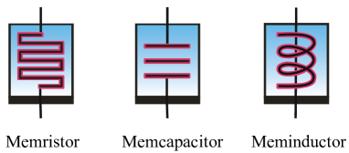
Figure 1 shows the circuit symbols of memristor, memcapacitor, and meminductor. The same symbols are used for memristive, memcapacitive, and meminductive systems. In the following sections we will discuss in detail these three memory elements and their properties. Since the majority of examples we provide in this review regard discrete memory elements, we will drop the word “discrete” in those cases, and explicitly specify when the elements are continuous or stochastic.
II.2 Hysteresis loops
Here, we point out that a distinctive signature of memory devices is a hysteresis loop. Such loops are very frequently reported in experimental papers when the response function or the function (or both) are plotted versus . The shape of a loop is determined by both the device properties and the input applied. In particular, it depends on both amplitude and frequency of the input. Therefore, the input should be fully specified when measurement results are reported, which is regrettably not always the case in the existing literature.
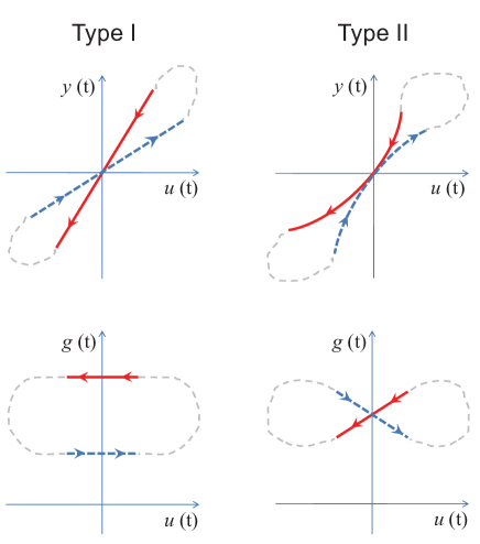
Let us now consider the situation in which hysteresis loops are well defined in the sense that and are periodic with a period of the applied ac voltage. This may not be always the case, for example, if equation (5) involves a stochastic component, or when the switching gradually occurs only in one direction. There are some common properties of these hysteresis loops. First of all, we note that as it follows from equation (4) for well-defined generalized response functions (by “well-defined” we mean and ), the function hysteresis loop passes through the origin ( is zero whenever is zero and vice versa). This is called a “pinched” hysteresis loop. A pinched loop may be “not self-crossing” or “self-crossing” (see figure 2).
The symmetry of equations (4-5) does not always define the type of crossing. However, as it follows from examples considered in this review, “not self-crossing” loops are very often observed when and are even functions of . We emphasize that this is not a necessary condition for “not self-crossing”. For instance, in the case of unipolar resistance switching (section III.2.2), and are even functions of , but hysteresis loops show “self-crossing”. In the opposite case, when is an odd function of , “self-crossing” behavior of curves is more common.
The feature of “not self-crossing” loops is observed, for example, in the case of thermistors and elastic memcapacitive systems (see, e.g., sections III.1 and IV.1.2). We define this hysteresis of type II crossing behavior because it normally results in a double loop in the response as a function of the input (see figure 2, right panel). The other type of hysteresis - shown in the left panel of figure 2 - involves typically a single loop in the response as a function of the input. Therefore, we call such a hysteresis of type I crossing behavior.
We also note that there are situations when the response function becomes zero or infinite when or as in the example of superlattice memcapacitive systems considered in section IV.2.1. In this situation, curves do not pass through the origin. Moreover, in some systems, additional crossings are possible at as in the case of ionic channels. We will discuss this example explicitly in section III.6.
II.3 Some remarks on time scales
The ability to categorize experimental systems as memristive, memcapacitive and meminductive in terms of general equations (4)-(5) (or their continuous and/or stochastic counterparts) provides the opportunity to understand some of their general properties following directly from the above mentioned equations. For clarity, let us consider discrete memory elements. The steady-state values of can be found as a solution of the algebraic equation
| (12) |
which follows from Eq. (5) assuming a constant value of the external control parameter and the existence of a steady-state. In particular, for non-volatile information storage, Eq. (12) should provide at least two possible solutions at .
Moreover, the magnitude of in Eq. (5) can be used to estimate the rates of change of the internal state variables or, in other words, the relevant time scales. This information is especially important for non-volatile memory applications when fast writing and reading time scales, as well as long-term data retention capability are required. Fig. 3 shows a sketch of a one-dimensional desirable for non-volatile information storage (for the sake of simplicity we assume that does not depend explicitly time ) evaluated at a certain value of selected between the minimum and maximum values of (assuming that such values do exist).
Generally, the function can be asymmetric with respect to , therefore, it can be reasonable to define ON and OFF write times separately. In particular, the writing time is of the order of
| (13) |
while the change of during the reading is of the order of
| (14) |
where is the read time. In addition, Eq. (14) can be used to determine the amount of read cycles before the device state is altered by consecutive read operation. Roughly, the allowed number of read operations is of the order of
| (15) |
We also note that sequential readings of information are not the only source leading to changes in the internal state of the device. In some cases, the state degradation can occur naturally, for example, because of diffusion or certain stochastic processes. Both these effects, in fact, can be taken into account explicitly using the formalism of stochastic memory circuit elements given in section II.1.
After these general considerations we are now ready to define the three different classes of memory elements.
II.4 Memristors and Memristive Systems
II.4.1 Definitions
The relation between the charge and the flux has been recognized long ago as a missing connection between the four different circuit variables Chua (1971). For the sake of this completeness let us then postulate a relation of the type
| (16) |
between the charge that flows in the system and the flux - which does not need to have a magnetic interpretation. The proportionality function is some response functional, with a time-dependent function to be specified later. Recalling that the flux is related to the voltage via
| (17) |
we can re-write equation (16) as
| (18) |
By differentiating the above relation with respect to time, and recalling that the current , we obtain
| (19) |
Let us now define the quantity
| (20) |
which has the dimensions of a resistance, so that equation (19) can be compactly written as
| (21) |
If the response depends only on the charge (), namely , the simple chain rule
| (22) |
with the functional derivative of with respect to the charge function , implies that equation (20) simplifies as
| (23) |
and equation (23) as
| (24) |
where the last step is a simple substitution of with the time integral of the current. The lower limit of integration can also be chosen zero provided . Equation (24) defines the relation between the current and voltage but unlike its ohmic counterpart, equation (1), it is non-linear and the function depends not just on the state of the system at a given time , but on the entire history of states through which the system has evolved. This is in fact explicit in the functional derivative of the response with respect to the charge dynamics .
Relation (24) is the definition of an ideal current-controlled memristor Chua and Kang (1976). It has become standard in circuit theory to represent it as in figure 1. It is clear that if the response function does not dependent on time, we find from equation (20) that also is independent of time, and equation (24) reduces to the ohmic form (1).
A memristor with depending only on the flux, that is , is instead called an ideal voltage-controlled memristor. It is described by
| (25) |
with the possibility of the lower limit of integration to be zero provided .
However, as we will discuss in the following sections, it may occur - and this is probably the norm rather than the exception in real systems - that the response function depends not just on the charge that flows across the system but also on one or more state variables that determine the state of the system at any given time. This could be, e.g., the position of oxygen vacancies in TiO2 thin films Yang et al. (2008), which determines the resistance of the film, or the temperature of a thermistor Chua and Kang (1976), or the degree of spin polarization in certain structures Pershin and Di Ventra (2008b); Pershin and Di Ventra (2009). Let us then group in the symbol the set of possible state variables (related to a particular device) of which we know their time evolution via the equation
| (26) |
where is a continuous -dimensional vector function. The relation between voltage and current can then be written as
| (27) |
and needs to be solved together with equation (26) for the state variables dynamics. These systems (with and/or depending on ) have been called current-controlled memristive systems Chua and Kang (1976). The voltage-controlled ones are those that satisfy the relations
| (28) | |||||
| (29) |
where is called the memductance (for memory conductance).
It might be well to point out that the classification of memristive systems (as well as memcapacitive and meminductive systems we discuss in the next sections) into current-controlled and voltage-controlled types is, in most cases, rather a matter of mathematical (or experimental) convenience. In particular, if we consider equation (27) describing a current-controlled memristive system and algebraically solve it with respect to the current (assuming a unique solution at any given time), then we actually get the equation (28) of the voltage-controlled memristive system. The second equation (29) can be obtained if we substitute obtained from equation (27) into equation (26). Thus, having equations of a current-controlled memristive system, we can re-write them in the form of a voltage-controlled one and vice-versa, provided that a unique solution of equation (27) with respect to the current, or a unique solution of equation (28) with respect to the voltage can be found.
As noted before, in real systems, it is very unlikely that the memristor’s state depends only on the charge that flows through the system or on the integral over the applied voltage. In other words, ideal memristors are probably rare - a notable exception is a small dissipative component in Josephson junctions, see section VI.2. That is possibly the reason why many authors use these words interchangeably so that the word “memristor” indicates any resistive system with memory that satisfies the coupled equations (27) and (26) or (28) and (29). In fact, even the authors of the paper Strukov et al. (2008) which has rejuvenated this field label their TiO2 device as memristor while, in reality, it is a memristive system. Actually, an attempt to describe the response of such memristive systems using the ideal memristor’s equation (24) or (25) can result in inadequate results, e.g., in switching at low applied biases or currents. The experimental evidence of ideal memristor behavior should contain, for instance, a plot showing a single (non-linear) curve when the device is driven by a periodic input. In this review, in order to avoid additional confusion, we will use the terms “memristor” and “memristive system” consistently with the definitions given above. The same will be applied also to ”memcapacitors” and ”memcapacitive systems” as well as to ”meminductors” and ”meminductive systems”.
II.4.2 Properties of Memristors and Memristive Systems
There are several properties that are relevant to identifying materials and systems as memristors or memristive. As anticipated in section II.2, arguably the most important one is the appearance of a “pinched hysteretic loop” in the current-voltage characteristics of these systems when subject to a periodic input Chua and Kang (1976). This is obvious from equations (27) and (26), because when then (and vice versa), as it is illustrated in figure 4. In addition, if the state equation (26) has a unique solution at any given time , if the voltage (or current) is periodic, then during each period the curve is a simple loop passing through the origin, namely there may be at most two values of the current for a given voltage , if we consider a voltage-controlled device, or two values of the voltage for a given current , for a current-controlled system.
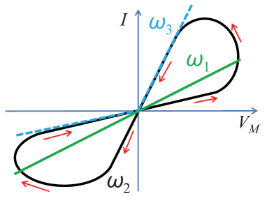
Moreover, when subject to a periodic stimulus, a memristive system typically behaves as a linear resistor in the limit of infinite frequency, and as a non-linear resistor in the limit of zero frequency (provided that in equation (26) has a steady-state solution) - see figure 4. These last two properties can be understood quite easily. Irrespective of the physical mechanisms that define the state of the system, at very low frequencies, the system has enough time to adjust its value of resistance to the instantaneous value of the voltage (or current), so that the device behaves as a non-linear resistor. On the other hand, at very high frequencies, there is not enough time for any kind of resistance change during a period of oscillations of the control parameter, so that the device operates as a usual (typically linear) resistor Chua and Kang (1976).
If , namely the resistance is positive at any given time, then the quantity (which is the energy stored in the system)
| (30) |
is always positive. In other words, the amount of energy removed from a memristive system cannot exceed the amount of previously added energy: memristors and memristive systems are passive devices. Typically, the electrical energy transforms into heat, which is then dissipated due to a heat exchange with the environment. Another important feature, that follows from the fact that the current is zero when the voltage is zero (and vice versa), is the so-called “no energy discharge property” namely a memristive system can not store energy, like a capacitor or an inductor. These are the main properties that we will use to identify memristive systems when discussing practical examples.
| Physical system | Thermistor |
|---|---|
| Internal state variable(s) | Temperature, |
| Mathematical description | |
| System type | First-order current-controlled memristive system |
II.4.3 Simple example: Thermistors
| Physical system | Thermistor |
|---|---|
| Internal state variable(s) | Temperature, |
| Mathematical description | |
| System type | First-order voltage-controlled memristive system |
Let us consider one of the first identified memristive systems: the thermistor. The latter one is a temperature-sensitive resistor. Although all resistances generally vary with temperature, thermistors are built of semiconducting materials that are especially sensitive to temperature, such as different oxides of metals including manganese, iron, nickel, cobalt, copper, and zinc. Memristive properties of thermistors are based on self-heating and were noticed by Chua and Kang in 1976 Chua and Kang (1976). To show that these are indeed memristive systems, let us consider a negative temperature coefficient (NTC) thermistor that is described by the current-voltage relation Sapoff and Oppenheim (1963)
| (31) |
where the constant denotes the resistance at a certain temperature , is the absolute temperature of thermistor (all temperatures are in Kelvin) and is a material-specific constant. It follows from equation (31) that the resistance of NTC thermistors decreases with temperature. The thermistor’s temperature depends on the power dissipated in the thermistor and is described by the heat transfer equation
| (32) |
where is the heat capacitance, is the dissipation constant of the thermistor Chua and Kang (1976), and is the background (environment) temperature. In the memristive description of thermistor, its temperature plays the role of the internal state variable. In order to obtain a memristive model of thermistor, we substitute from equation (31) into equation (32). Table 1 summarizes the memristive model of thermistor.
As an example of the previously mentioned equivalence of current-controlled and voltage-controlled memristive system’s formulations, we would like to demonstrate that the thermistor can alternatively be described as a voltage-controlled memristive system. For this purpose, we can express the current from equation (31) and substitute it into equation (32). Table 2 provides a description of thermistor as a voltage-controlled memristive system. Such a transformation between current-controlled and voltage-controlled description and vice-versa can be easily performed for many systems. Therefore, in the following, we will avoid giving a dual description, since very often the transformation between different descriptions is trivial.
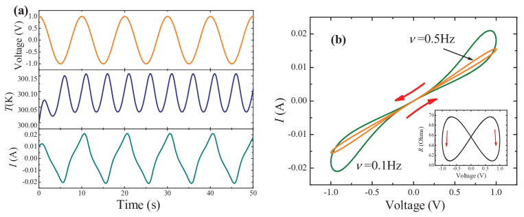
Figure 5 illustrates a solution of the equations given in table 2. It is worth noting that, because of the symmetry of the equation for the internal state variable with respect to the change of the voltage sign, the lines in figure 5(b) do not self-intersect when passing through (0,0) and, therefore, are of type-II crossing behavior (cf. figure 2). This is an interesting distinctive feature of thermistor’s pinched hysteresis loops compared to others we will discuss later. We also note that the curves for the thermistor demonstrate frequency-dependent hysteresis typical of memristive systems.
II.5 Memcapacitors and Memcapacitive Systems
II.5.1 Definitions
Let us now extend the above concept of resistor with memory to the other two fundamental circuit elements, namely capacitors and inductors, and define corresponding memory circuit elements Di Ventra et al. (2009). It is worth pointing out that for these memory elements a microscopic derivation based on response functions has not been developed yet. We thus follow the axiomatic definitions of reference Di Ventra et al. (2009). We will then show in the following sections that several systems do indeed fall within these classifications.
From equations (4) and (5) we define a voltage-controlled memcapacitive system by the equations
| (33) | |||||
| (34) |
where is the charge on the capacitor at time , is the corresponding voltage, and is the memcapacitance (for memory capacitance) which depends on the state and history of the system, as it is evident in its dependence on the state variables . The relation
| (35) | |||||
| (36) |
defines a charge-controlled memcapacitive system, where is an inverse memcapacitance.
A subclass of the above systems corresponds to the case in which the capacitance depends only on the full history of the voltage, namely
| (37) |
This equation defines an ideal voltage-controlled memcapacitor. In this case, equations (33) and (34) reduce to
| (38) |
Similarly, for a charge-controlled memcapacitor
| (39) |
where in the above two equations, the lower integration limit (initial moment of time) may be selected as , or 0 if (in equation (38)) and (in equation (39)).
We note that in this review (similarly to the reference Di Ventra et al. (2009)) the name “memcapacitor” will be reserved for the special class defined by equation (38) or equation (39) which represent ideal memory capacitors and the term “memcapacitive systems” will be used for the broader class of elements defined by equations (33) and (34). Similarly to the case of memristive systems, we expect memcapacitive systems to be the norm rather than the exception. For the sake of clarity, we will not use the terms ”memcapacitor” and ”memcapacitive systems” interchangeably.
II.5.2 Properties of Memcapacitors and Memcapacitive Systems
It follows from equation (33) or (35) that, apart from specific cases that we will discuss later (see, e.g., section IV.2.1), the charge is zero whenever the voltage is zero. Note, however, that in this case, does not imply (and vice versa), and thus this device can store energy. Therefore, the latter can be both added to and removed from a memcapacitive system. However, unlike memristive systems, it is easy to see that in the present case the relation
| (40) |
does not always hold. This implies that equations (33) and (34) or equations (35) and (36) for the memcapacitive systems postulated above may, in principle, describe both active and passive devices. To see this point more clearly consider figure 6 where a schematic memcapacitive system hysteresis loop passing through the origin is shown when the system is subject to a periodic stimulus of period . The shaded areas give the energies
| (41) |
and
| (42) |
added to or removed from the system, respectively, when the integral runs over half of the period. The memcapacitive system can then be
| (43) |
| (44) |
or
| (45) |
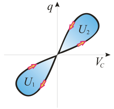
The fact that a memcapacitive system may be dissipative can be seen by looking at a practical realization of memory capacitance. This can be accomplished in two different ways, or their combination. The simplest realization is via a geometrical change of the system (e.g., a variation in its structural shape like in nano-electromechanical systems Evoy et al. (2004)). Alternatively, one may rely on the quantum-mechanical properties of the free carriers and bound charges of the materials composing the capacitor that could give rise, for instance, to a history-dependent permittivity . In either case, inelastic (dissipative) effects may be involved in changing the capacitance of the system upon application of the external control parameter, whether charge or voltage. These dissipative processes release energy in the form of heating of the materials composing the capacitor. We will discuss some of these cases in section IV.
On the other hand, an active device may be realized when, in order to vary the capacitance, one needs energy from sources that control the state variable dynamics, equation (34), other than the energy from the control parameter. This energy could be, e.g., in the form of elastic energy or provided by a power source that controls, say, the permittivity of the system via a polarization field. This energy can then be released in the circuit thus amplifying the current.
Memcapacitive systems share with memristive systems the property that they typically behave as linear elements in the limit of infinite frequency, and as non-linear elements in the limit of zero frequency, assuming that equations (34) and (36) admit a steady-state solution. The origin of this behavior rests again on the system’s ability to adjust to a slow change in bias (for low frequencies) and its inability to respond to extremely high frequency oscillations.
In addition, if the state equation (34) has only a unique solution at any given time , then if is periodic, the curve is a simple loop during a period (as that shown in Fig 6), namely there may be at most two values of the charge for a given voltage , for a voltage-controlled device, or two values of the voltage for a given charge , for a charge-controlled system. This loop is also anti-symmetric with respect to the origin if, for the case of equations (33) and (34), and .
Finally, we anticipate an important point we will come back to in sections II.8 and IV.2.1. Equations (33) and (34) for memcapacitive systems say nothing about whether these devices may or may not be constructed as a combination of the basic circuit elements (resistors, capacitors and inductors) and elements that can, in fact, be derived from these.
Furthermore, some of these memcapacitive systems show interesting features which are evident from the definition (33) and (34). In fact, there may be cases in which, at certain instants of time, both the charge and the capacitance are zero, and thus the voltage across the capacitor may be finite. Similarly, there may be times when the capacitance diverges while the voltage vanishes Martinez-Rincon et al. (2010); Krems et al. (2010). This gives rise to a finite charge on the plate of the capacitor. Finally, nothing in the definition (33) and (34) prohibits the voltage to change sign while the charge does not. This situation represents the case of dynamical over-screening and produces a negative capacitance Martinez-Rincon et al. (2010); Krems et al. (2010), and this may occur without the need of, e.g., ferroelectric materials.
II.5.3 Simple example: elastic memcapacitive system
Let us consider a model of a simple electro-mechanical device with memory, we call elastic memcapacitive system. Some authors also call such a system an elastic capacitor Partensky (2002). An elastic memcapacitive system is a parallel-plate capacitor with an elastically suspended upper plate and a fixed lower plate as shown in figure 7. When a charge is added to the plates, the separation between plates changes as oppositely-charged plates attract each other. The dynamics of the system depends on initial conditions and time-dependent fields thus providing a memory mechanism. Previously, the model of elastic memcapacitive system was used in studies of lipid bilayers and to explain electrical breakdown of biological membranes Crowley (1973); Partensky (2002). From the memory elements standpoint, the elastic memcapacitive system is an important example of passive memcapacitive device.
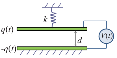
The internal state variable of the elastic memcapacitive system is the displacement of the upper plate from its equilibrium uncharged position, , under the action of a Coulomb interaction of oppositely charged plates. Mathematically, the charge dynamics on the elastic memcapacitive system is described by a parallel-plate capacitor model with variable separation between the plates
| (46) |
where is the equilibrium capacitance at , and the dynamics of is given by the classical harmonic oscillator equation including damping and driving terms:
| (47) |
Here, is a damping coefficient representing dissipation of the elastic excitations, , is the spring constant, is the upper plate’s mass, is the plate’s area. It follows from equations (46-47) that the elastic memcapacitive system is a second-order charge-controlled memcapacitive system. It is dissipative when and non-dissipative when . The model of elastic memcapacitive system is summarized in the table 3.
| Physical system | Elastic memcapacitive system |
|---|---|
| Internal state variable(s) | Displacement and velocity of upper plate, |
| , | |
| Mathematical description | |
| System type | Second-order charge-controlled memcapacitive system |
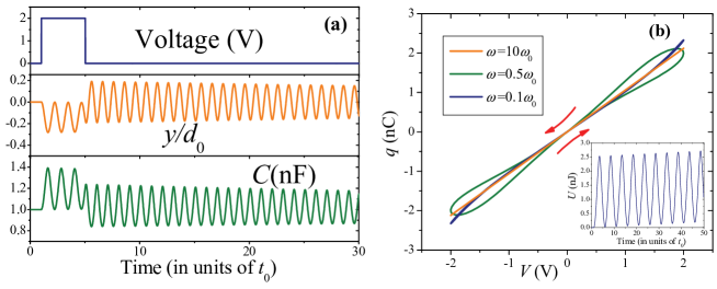
Figure 8 shows simulations of the elastic memcapacitive system. When a single voltage pulse is applied to the elastic memcapacitive system (figure 8(a)), the upper plate begins oscillating. These oscillations last for an extended period of time keeping the memory about the pulse. In the equation of motion for the state variable (equation (47)), the driving force is proportional to . As a consequence, the hysteresis curves of the elastic memcapacitive system (Fig. 8(b)) do not self-intersect at (0,0), namely they are of type II, similar to the curves of thermistor (section II.4.3, see also figure 2).
II.6 Meminductors and Meminductive Systems
II.6.1 Definitions
Let us now introduce the third class of memory devices, namely that of memory inductors Di Ventra et al. (2009). In order to do this, let us first define the flux
| (48) |
where is the induced voltage on the inductor (equal to minus the electromotive force). In analogy with memristive and memcapacitive systems we then define from equations (4) and (5) a current-controlled meminductive system one that follows the relations
| (49) | |||||
| (50) |
where is the meminductance. Similarly, we define a flux-controlled meminductive system the following
| (51) | |||||
| (52) |
with the inverse of the meminductance.
In this work, we will not use interchangeably the terms “meminductive system” and “meminductor”, reserving the latter for ideal meminductors Di Ventra et al. (2009). Those are a subclass of the above systems, when equations (49) and (50) reduce to
| (53) |
for a current-controlled system, or when equations (51) and (52) can be written as
| (54) |
for a flux-controlled meminductor. In the above two equations, the lower integration limit may be selected as , or 0 if and , respectively.
II.6.2 Properties of Meminductors and Meminductive Systems
Meminductors and meminductive systems share essentially the same properties of memcapacitive systems, such as an hysteretic loop that may or may not be pinched - and situations in which the meminductance may diverge and become negative, see, e.g., equations (49) and (50) - non-linearity at very low frequencies and linearity at high frequencies, energy storage, and the possibility to represent passive, dissipative or active elements.
The energy stored in the system can be evaluated as follows. For the sake of definiteness, let us consider only the current-controlled meminductive systems. Taking first the time derivative of both sides of equation (49) yields
| (55) |
which shows that the second term on the right-hand side of the above equation is an additional contribution to the induced voltage due to a time-dependent inductance . The energy stored in the current-controlled meminductive system can then be calculated as
| (56) |
When the inductance, , is constant, we readily obtain the well-known expression for the energy . This is interpreted as the energy of the magnetic field generated by the current. However, in the meminductive case, the extra term due to the time derivative of may be related to other processes that control the meminductance and which are formally represented by the state variables . These processes could be related, for instance, to the elastic energy required to modify the shape of the inductor in time, or an external energy source that controls the permittivity of the inductor as a function of time.
In general, we can formulate the passivity criterion of meminductive systems by stating that if at they are in their minimal energy state then at any subsequent moment of time, with the inequality sign indicating the presence of energy storage and dissipative processes.
II.6.3 Simple example: elastic meminductive system
(a)
(b)
 (c)
(c)
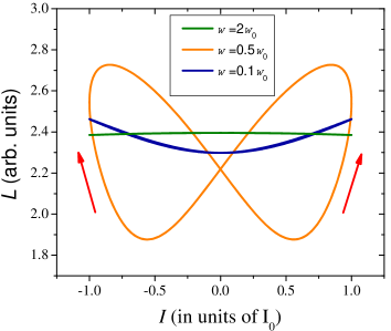
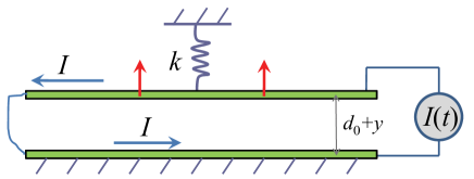
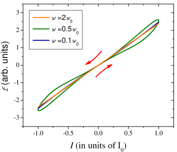
We here introduce the model of elastic meminductive system, namely an inductor which is formed by two parallel wires of length separated by a distance as we depict in figure 9(a). One of the wires is kept fixed while the other is allowed to move under the effect of a spring, and we assume for simplicity that both wires have the same radius . The two wires are connected together as illustrated in figure 9(a) in such a way that they carry currents of equal magnitude but opposite direction. This system can in principle be realized using micro-electromechanical systems (MEMS) as we will discuss in section V.1. As current flows through the wires, the repulsive magnetic force pushes the top wire up compressing the spring. In this way, the distance between the wires increases resulting in a different value of inductance according to the equation
| (57) |
where is the vacuum permeability, is the equilibrium distance between the wires when , and is the displacement of the top wire from its equilibrium position at .
The classical equation of motion of the top wire, taking into account damping and the currents interaction force, can be written as
| (58) |
Here, is a damping coefficient representing dissipation of the elastic excitations, , is the spring constant and is the upper wire’s mass. It follows from equation (58) that the elastic meminductive system is a second-order current-controlled meminductive system. Its properties are presented in table 4.
| Physical system | Elastic meminductive system |
|---|---|
| Internal state variable(s) | Displacement and velocity of upper wire, |
| , | |
| Mathematical description | |
| System type | Second-order current-controlled meminductive system |
It is dissipative when , and non-dissipative when . The overall form of the equation describing dynamics of elastic meminductive system (Eq. (58)) is similar to that of elastic memcapacitive system (47), with the difference that the interaction in the case of the meminductive system is repulsive and depends on the wires’ separation (in the case of elastic memcapacitive system, the interaction force is attractive and does not depend on the separation between the plates).
Selected results of elastic meminductive system’s simulations are presented in figure 9(b,c). These plots demonstrate typical frequency dependencies of memory elements. It is interesting to note the absence of self-crossing in the curves, and a self-crossing of curves. Therefore, following our suggested classification scheme, such a system shows a type-II hysteresis.
II.7 Combination of memory features
At this stage it is worth pointing out that in real systems, the above three memory features may appear simultaneously Di Ventra et al. (2009); Martinez-Rincon et al. (2010); Driscoll et al. (2009b). This is not surprising, especially at the nanoscale. To give just an example we recall that when a current flows in a resistor, at the microscopic level local resistivity dipoles form due to scattering of carriers at interfaces Landauer (1957). Namely, charges accumulate on one side of the resistor with consequent depletion on the other side, with possible accumulation and depletion over the whole spatial extent of the resistor Di Ventra (2008). It was shown numerically that these dipoles develop dynamically over length scales of the order of the screening length Sai et al. (2007). This means that the formation of these local resistivity dipoles takes some time and is generally accompanied by some energy storage related to the capacitance of the system. It is also known that memristive and memcapacitive effects can be simultaneously observed in the resistance switching memory cells Liu et al. (2006). The experimental data reproduced in Figure 10 from reference Liu et al. (2006) clearly show that the changes in memristance and memcapacitance are correlated and, therefore, in this example they are most probably related to the same state variables.
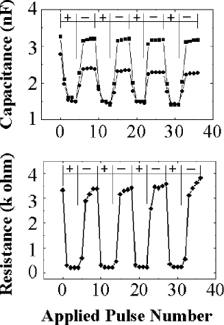
We thus expect that in nanoscale systems memristive behavior is always accompanied to some extent by a (possibly very small) capacitative behavior. In this case the I-V hysteresis loop may not exactly cross the origin at frequencies comparable to the inverse characteristic time of charge equilibration processes. We will give explicit examples of this effect in section III.5.1 when discussing the transverse voltage memory response of the spin Hall effect in inhomogeneous semiconductor systems Pershin and Di Ventra (2009), and in section IV.3.2, where the memristance and memcapacitance induced by the metal-insulator transition of VO2 is made clear in the optical response of metamaterials Driscoll et al. (2009b).
The analysis of these systems may be done by combining a number of three memory circuit elements in parallel and/or in series, possibly together with standard resistors, capacitors and inductors. It is worth mentioning that combination of these elements may result in compact descriptions of memory systems with non-algebraic dependence on the control parameters. As an example of this, let us consider a voltage-controlled memristive system (described by equations (28) and (29)) and a voltage-controlled memcapacitive system (equations (33) and (34)) coupled in parallel (see figure 11).
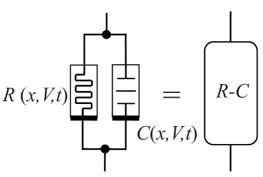
For simplicity we may assume that the same state variables determine the memory of both the resistor and the capacitor. This, however, may not always hold. This latter case, however, can easily be accounted for by expanding the range of state variables to include both sets. Using Kirchhoff’s law, the total current of the parallel circuit is
| (59) |
where we indicate with the current that flows across the memristive system. Introducing the definitions of the two memory elements (and noticing that in a parallel circuit the voltage drop across the resistor is the same as that across the capacitor) we then get
| (60) |
By defining the effective memductance
| (61) |
we find that the whole circuit behaves like a voltage-controlled memristive system with current
| (62) |
and non-algebraic dependence on the bias .
Along similar lines, Mouttet Mouttet (2010) has suggested a memadmittance (memory admittance) model in order to describe simultaneous memristive and memcapacitive properties of a system. This idea was applied to thin-film memory materials. Based on this approach, equations relating the cross-sectional area of conductive bridges in resistive switching films to shifts in capacitance were derived Mouttet (2010). Moreover, Riaza Riaza (2010) has proposed a hybrid memristor that is described by a relation involving all four circuit variables , , and . Such an element may account for physical devices in which memory effects of different nature coexist. Several examples of hybrid memristors as well as corresponding extension of circuit theory is given in his work Riaza (2010).
II.8 Are memristors, memcapacitors and meminductors fundamental circuit elements?
Finally, it is worth mentioning that the behavior of an ideal memristor, namely that which is described by the relation (24) (or equation (25)) cannot be simulated by any combination of “standard” - namely two-terminal, time-independent, albeit possibly non-linear - resistors, capacitors and inductors. In other words, there is no possible finite combination of standard circuit elements that can reproduce the dynamical properties of ideal memristors. This can be shown by recalling that a memristor does not store energy so that capacitors and inductors cannot possibly be used to simulate it, while a finite number of non-linear resistors cannot reproduce, e.g., the current history as required by the definition (24). It is for this reason that an ideal memristor is sometimes called the “fourth” circuit element Chua (1971).
However, also an ideal memcapacitor and an ideal meminductor (see, e.g., equations (39) and (53)) cannot be simulated by combinations of standard resistors, capacitors and inductors, because in this case as well, the lack of time dependence does not allow to retain information on the full charge (memcapacitor) or current (meminductor) dynamics. For instance, one could argue that since standard capacitors store information on the current history (the integral of the current is the charge on the capacitor) they could be used to simulate the behavior of meminductors. However, if this were the case, the resulting circuit would have capacitative components and therefore would not be an ideal meminductor. The same reasoning can be made for using inductors to simulate memcapacitors.
Therefore, it is in this sense that ideal memristors, memcapacitors and meminductors can be considered as “fundamental” circuit elements, and it would thus be tempting to call the last two the “fifth” and “sixth” circuit elements. These authors, however, do not share this view, and prefer to subscribe to the notion that there are only three fundamental circuit elements: resistors, capacitors and inductors, with or without memory.
We also note that the above considerations can not be extended to memristive, memcapacitive and meminductive elements because in that case, the internal state variables could have a physical origin which could be simulated by standard (possibly non-linear) circuit elements. For instance, as we will discuss in section IV.2.1, some memcapacitive systems may be represented by a combination of basic circuit elements (capacitors and non-linear resistors; for examples of these, see, e.g., references Krems et al. (2010); Martinez-Rincon et al. (2010)). Or one could envision a combination of non-linear resistors with negative differential resistance Sze and Ng (2006) to retain the history of the voltage or current and thus simulate memristive systems. Irrespective, these types of memory elements are still of great importance since they provide a complex functionality within a single electronic structure Martinez-Rincon et al. (2010).
After these general considerations we are now ready to discuss several systems that exhibit memory features and the physical mechanisms that generate these phenomena.
III Memristive systems
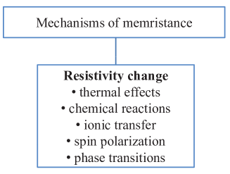
Many systems exhibit memristive behavior whose underlying physical mechanisms vary considerably (see figure 12 for a list of common mechanisms). Examples that were identified early in reference Chua and Kang (1976) include thermistors Sapoff and Oppenheim (1963) and ionic systems, in particular membranes in neuron cells Hodgkin and Huxley (1952). For the reasons we have anticipated in section I, recent interest has been focused on the dynamics of nanostructures. Some of them were intensively studied in the context of the development of resistive-switching memory during the last 10-15 years. To the best of our knowledge, this area of research was initiated by Hickmott in 1962 by observing hysteretic behavior in oxide insulators Hickmott (1962). Later, resistance switching was demonstrated in thin films of silicon monoxide (SiO) between metal electrodes by Simmons and Verderber Simmons and R (1967) and in TiO2 by Argall Argall (1968). (These and other earlier works in the field were reviewed by Dearnaley et al. Dearnaley et al. (1970).) However, it was only in 2008 that resistive switching devices were recognized as memristive systems Strukov et al. (2008). Additional examples of memristive systems include spintronic devices Pershin and Di Ventra (2008b); Wang et al. (2009), phase-transition materials Driscoll et al. (2009b, a) and polaronic systems Alexandrov and Bratkovsky (2009). Below we discuss memristive properties of a variety of physical systems in details.
III.1 Thermistors
Thermistors were considered in section II.4.3, and we refer the reader to that section for details on a mathematical model to describe them.
III.2 Resistance Switching Memory Cells
At the present time, it is well known that resistive switching effects can be observed in such diverse classes of materials as binary oxides (TiO2, CuO, NiO, CoO, Fe2O3, MoO, VO) Yang et al. (2008); Inoue et al. (2008); Lee et al. (2007); Seo et al. (2004); Shima et al. (2007); Driscoll et al. (2009b, a), nanogap systems on SiO2 Yao et al. (2009), metal nanogap junctions Naitoh et al. (2006), perovskite-type oxides (Pr1-xCaxMnO3, SrTiO3:Cr) Asamitsu et al. (1997); Fors et al. (2005); Kim et al. (2006b); Meijer et al. (2005); Nian et al. (2007), sulfides (Cu2S,Ag2S) Terabe et al. (2005); Tamura et al. (2006); Waser and Aono (2007), semiconductors (Si, GaAs, ZnSe-Ge) Jo and Lu (2008); Dong et al. (2008); Jo et al. (2009) and organics Stewart et al. (2004); Lai et al. (2005); Ling et al. (2008). The basic mechanisms of switching are not yet well understood in all cases, however, quite generally, the related memory devices can be separated into the following most important categories: nanoionic, nanothermal (a sub-class of nanothermal memory devices, phase-change memory cells, are considered in section III.3), macromolecular memory and molecular effects memory devices ITRS. The International Technology Roadmap for Semiconductors - ITRS 2009 Edition. http://www.itrs.net . Due to this wide range of physical systems and memory mechanisms, we will provide specific examples with particular focus on the state variables responsible for memory and their theoretical description, if available. The reader interested in some more comprehensive reviews on just resistive switching is urged to look into the recently published ones Waser and Aono (2007); Scott and Bozano (2007); Sawa (2008); Karg et al. (2008); Waser et al. (2009).
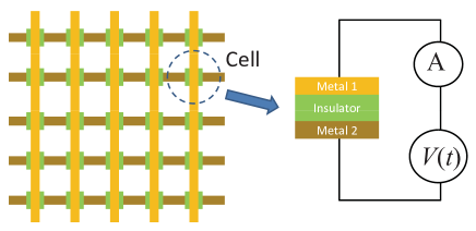
Very often, the experimental setup showing resistive switching involves an array (called a crossbar array) of capacitor-like cells. Each capacitor-like cell contains a layer of an insulating material sandwiched between two metal layers (which may be made of the same or different materials) as depicted in figure 13. In what follows, we will discuss behavior of separate cells. Although each cell in the crossbar architecture can be addressed independently by an appropriate selection of a word (say, horizontal) and bit (vertical) lines, the current between such two lines can flow across many paths causing a potential problem for the crossbar memory implementation. As a possible solution of this problem, additional individual access devices (such as transistors or diodes) may be required.
Typically, an as-fabricated cell is in a highly-resistive state and, in order to obtain resistance switching operation, an electroforming step is needed. This is an important step of device fabrication defining its future operation Jeong et al. (2009a). In this step, a high voltage amplitude pulse is applied to the cell producing a nondestructive (soft) breakdown, with the creation of single “filaments” inside the main material matrix. This process of breakdown is usually controlled by selecting a compliance current value (namely a threshold current of the external input) that induces, at least in some cases, the desired switching effect Jeong et al. (2007); Do et al. (2009). For example, the authors of reference Jeong et al. (2007) have observed that the electroforming of a Pt/TiO2/Ti structure with a lower compliance current (0.1 mA) results in a bipolar hysteresis while a higher compliance current (1-10 mA) leads to unipolar resistance switching (the meaning of these two types of hysteresis will become clear in a moment). A detailed experimental study of the electroforming process in TiO2 was reported recently Yang et al. (2009). The dielectric breakdown in SiO2 was investigated in Li et al. (2008). A deficiency of oxygen atoms along the breakdown path was observed, caused by large currents through the percolation path. As a result, it is believed that the local energy gap could have collapsed after the removal of oxygen atoms with consequent rearrangement of local atomic structure Li et al. (2008).
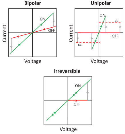
Let us now consider the different types of resistance switching reported in the literature. Figure 14 illustrates the three most general behaviors: bipolar, unipolar, and irreversible. Such a classification of curves can be used in addition to the categorization in terms of the crossing type at the origin suggested in section II.2. Below we will consider these three cases in more detail.
III.2.1 Bipolar resistance switching
In the case of bipolar switching both voltage polarities are required to switch a device from a low resistance state (ON) to a high resistance state (OFF) and back. A typical shape of curve in the case of bipolar switching as shown in figure 14 provides just a general topology of these curves. Experimentally measured loops depend on both the system type and measuring conditions, and can be thus quite different from this ideal topology. In the bipolar case the hysteresis process often is of a threshold type: while a high applied voltage is needed to change the device state, at low applied voltages the resistance of the device remains unchanged. This is very often associated with ionic transport and electrochemical reactions, even though the exact experimental cause is not always clear and may originate from a combination of effects Waser and Aono (2007). Moreover, we note that in most cases the switching has a gradual character: the change of, say, resistance of a device proceeds continuously (not as an abrupt jump between two limiting values). Such a property is promising for multi-state memory in which a single memory cell can store several bits of information.
We now consider several examples of bipolar switching observed in devices fabricated from different materials. Our first example is a titanium dioxide (TiO2) thin film sandwiched between metal electrodes (see figure 15). This resistive feature has been known since 1968 Argall (1968). Recently, however, the switching behavior of this binary oxide has been explained within the context of a memristive model Strukov et al. (2008); Yang et al. (2008). In the case of Pt/TiO2/Pt, it was suggested that the switching involves changes in the electronic barrier at the Pt/TiO2 interface induced by drift of oxygen vacancies under an applied electric field. When vacancies drift towards the interface, they create conducting channels that short-circuit the electronic barrier. When vacancies drift away from the interface they eliminate these channels, restoring the original electronic barrier Yang et al. (2008). This explanation, however, has been recently challenged Wu and McCreery (2009). In this alternative explanation, the conductivity change of TiO2 is associated with an electrochemical reduction of Ti oxide to the much more conductive Ti oxide, analogous to a solid-state redox reaction Wu and McCreery (2009). A similar reaction-based mechanism taking place at the interface between Pt and TiO2 was considered in reference Jeong et al. (2009b). The authors of this work state that the electrochemical reactions modulating the Schottky barrier height at the interface play the dominant role in the device behavior.
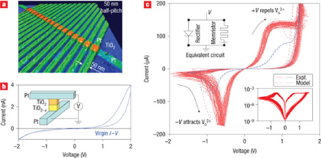
Irrespective of the basic physical mechanism at play, this material demonstrates promising characteristics for future ultra-high density memory applications such as fast read/write times (10ns), high ON/OFF ratios (), suitable range of programming voltages, and possibility to fabricate small size cells. The latter, in particular, is viewed as an advantage in fabricating high-density neuromorphic circuits, namely circuits that simulate neurological functions, because of the possibility to reach structure densities comparable (or even larger) than the density of neurons and synapses (connections among neurons) in the human brain. We will come back to this type of applications in section VII.2.1.
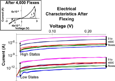
An interesting TiO2-based device is a flexible memristive system as presented in reference Gergel-Hackett et al. (2009). This device was fabricated on an HP laser-jet transparency using an inexpensive room temperature solution processing. The device demonstrates ON/OFF ratios larger than , about s memory storage potential, and the ability to operate after being physically flexed 4000 times Gergel-Hackett et al. (2009). Multiple consecutive mechanical deformations of the device lead to an increase of resistance in both ON and OFF states, while keeping ON/OFF ratios almost unchanged (see figure 16). Such devices have the potential for use in flexible lightweight portable electronics Gergel-Hackett et al. (2009).
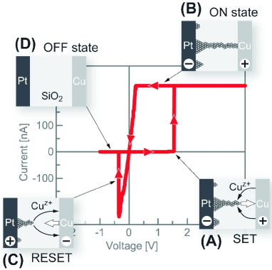
In nanoionics-based memories Waser and Aono (2007), a memory cell is composed by a couple of metal electrodes separated by a thin film of insulating material playing the role of solid-state electrolyte, such as an oxide NiO Seo et al. (2004), SiO2 Schindler et al. (2007); Schindler et al. (2009a), SrTiO3 Szot et al. (2006) or higher chalcogenides - Ag2S Terabe et al. (2005), GexSe Kozicki et al. (2005); Schindler et al. (2009b). One of the electrodes is made of a relatively inert metal (such as Pt) and the other electrode is electrochemically active (e.g., Ag or Cu). A negative bias applied to the inert electrode forces a flow of metal ions in the electrolyte (originating from the now-positive active electrode) toward the inert metal electrode. After a short period of time these ions compose a filament that connects two metal electrodes. This filament dramatically reduces the resistance of the cell. Applied bias of the opposite polarity drifts the active electrode ions in the opposite direction destroying the filament. The basic scheme of operation of such a cell is shown in figure 17. Such memory technology is often called programmable metallization cell (PMC) Kozicki et al. (2005) or electrochemical metallization cell (ECM) or CBRAM (conductive-bridging random access memory) Dietrich et al. (2007). In figure 17 we show a pinched I-V hysteresis curve observed in Cu-SiO2-based electrochemical metallization memory cells. This figure also shows dynamics of filament formation.
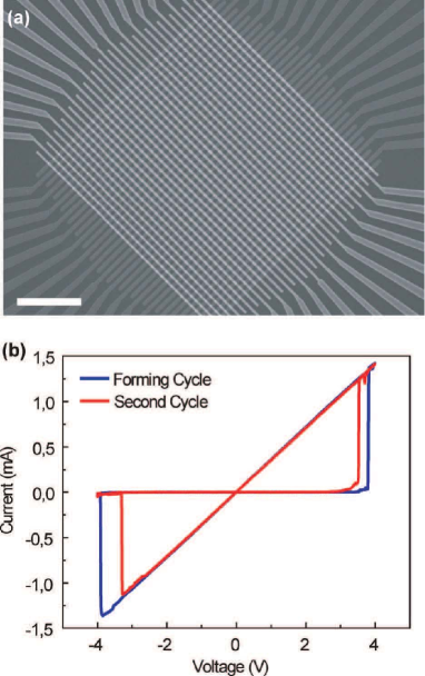
Recently, nanoionic resistive switching in silicon-based materials was experimentally demonstrated Jo and Lu (2008); Dong et al. (2008); Jo et al. (2009). In these experiments, amorphous-Si is used as the switching medium, one of the electrodes is metallic (typically Ag), and the other electrode is p-type Si. In this case the hysteresis is explained by the formation of conductive filaments consisting of Ag particles inside the amorphous-Si. A filament growth is a step-by-step process by which a new Ag particle hops into a new trapping site. Such devices are CMOS (complementary metal oxide semiconductor) compatible, and offer promising characteristics such as fast writing (10ns), reasonable endurance ( cycles) and good retention time ( years). Moreover, a high-density crossbar array based on such materials was fabricated Jo et al. (2009). In figure 18 we show an image of this array as well as the characteristics of a single cell. Such a structure exhibits a symmetric bipolar switching together with a high ON/OFF conductance ratio.
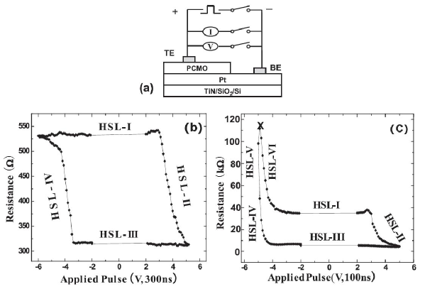
The mechanism of hysteresis in perovskite oxide films Pr0.7Ca0.3MnO3 (PCMO) was recently investigated Nian et al. (2007); Rozenberg et al. (2010). These materials show a bipolar switching as we demonstrate in figure 19. The authors of Ref. Nian et al. (2007) suggest an oxygen vacancies diffusion model to explain the hysteresis phenomenon. Within this model, a switching pulse results in a pileup of oxygen ions near metal electrodes thus changing the resistance. Moreover, it is proposed that this mechanism can explain the resistance switching in binary transition-metal oxides and other complex oxides as well. The authors of Ref. Rozenberg et al. (2010) suggest a discrete vacancies diffusion model. Their study underlines the important role of highly resistive dielectric-electrode interfaces and shows a qualitative agreement with experimental data.
Bipolar resistance switching is also observed in structures containing organic materials (see, e.g., references Stewart et al. (2004); Cai et al. (2005); Lai et al. (2005)), although its origin is not yet fully understood. In particular, Stewart et al. Stewart et al. (2004) have demonstrated that hysteresis characteristics of different molecular materials sandwiched between Pt and Ti electrodes are very similar suggesting a molecular-independent hysteresis mechanism. Moreover, they have shown that in a structure with similar (Pt) electrodes the switching becomes irreversible. The authors suggest Stewart et al. (2004) that a possible reason could be related to formation of electromigration-induced filaments, or incomplete electrochemical reaction of one electrode and the molecular monolayer Stewart et al. (2004).
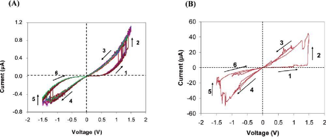
Cai et al. Cai et al. (2005) have reported a reversible hysteresis in nanoscale thiol-substituted oligoaniline molecular junctions. In their experiments, the switching occurs at V threshold voltage, with a high-to-low conductance ratio of up to 50, and high-state storage times much longer than 22 hours. In figure 20 we show selected results of their measurements. These authors have concluded that reversible bistable switching in their experimental system is an inherent molecular phenomenon, most likely arising from a concerted shift in charge delocalization and molecular conformation when the applied voltage across the molecular junction exceeds a critical threshold value Cai et al. (2005).
III.2.2 Unipolar resistance switching
The unipolar switching (see figure 14) is considered by some authors to be based on a thermal effect Waser and Aono (2007). The switching is defined by two voltages: the set (driving OFFON transition), and the reset (driving ONOFF transition) voltages (see figure 14). The set voltage is always higher than the reset one. Physically, in samples with this type of hysteresis, a weak conducting filament with a controlled resistance is formed in the electroforming process. During the reset operation, this filament is partially destroyed because of the large amount of heat released, similarly to a traditional household fuse Waser and Aono (2007). In the set operation, the filament is reconstructed again. The nanoscale filament formation was recently observed experimentally in such materials as TiO2 Choi et al. (2005) and NiO Kim et al. (2006a).
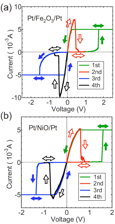
In figure 21 we show examples of unipolar switching behavior observed in metal/binary-transition-metal oxides/metal structures based on Fe2O3 and NiO Inoue et al. (2008). In order to clarify the hysteresis mechanism, the authors of reference Inoue et al. (2008) have studied several different structures, in particular varying a top Pt electrode area. They found that in the ON state the current does not depend on the area of the top electrode, while in the OFF state the current is proportional to the top electrode area. Based on these findings they have suggested a “faucet” model of resistance switching in which an “electric faucet” opens/closes in one or both interfaces between metal electrodes and oxide when the device switches into the ON/OFF state Inoue et al. (2008). However, a complete understanding of this effect is still lacking.
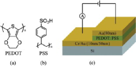
Our next example is the unipolar switching in a polymer material poly(3,4-ethylene-dioxythiophene):polystyrenesulfonate, commonly referred to PEDOT:PSS. The hysteresis mechanisms in PEDOT:PSS are still generally unknown, and those suggested in the literature are highly speculative Liu et al. (2009). This material, in fact, can exhibit all types of switching behavior shown in figure 14, depending on the type of material electrodes used. Moller et al. Moller et al. (2003) have observed an irreversible switching in a Au/PEDOT:PSS/Si p-i-n diode structure. In experiments with ITO/PEDOT:PSS/Al devices Ha and Kim (2008), bipolar switching characteristics were observed. Finally, in recent papers Liu et al. (2009); Ha and Kim (2009) studying Au/PEDOT:PSS/Au and Al/PEDOT:PSS/Al structures, respectively, the unipolar switching was reported.
 (d)
(d)
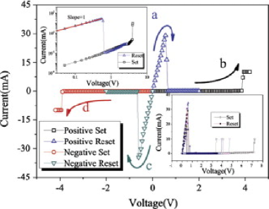
We show switching characteristics of a Au/PEDOT:PSS/Au device Liu et al. (2009) in figure 22. In this plot, the sweep sequence is indicated by the alphabet letters. The probable mechanism in this case is the forming and rupture of conductive paths, presumably related to the oxidation and reduction of the PEDOT:PSS film Liu et al. (2009). A resistive ratio of 103 and no significant degradation over s under continuous readout testing were found.
III.2.3 Irreversible resistance switching
The third type of switching, the irreversible switching, is of little interest from the point of view of memristive systems since in this case the initially fabricated device can only be switched toward a different state irreversibly (only in one direction). However, it is evident that these devices are memristive since the resistance at any given moment of time is defined by the history of the system (e.g., voltages applied to the device in the past). Of course, some typical features of memristive systems such as repeatable hysteresis loops can not be observed with such devices.
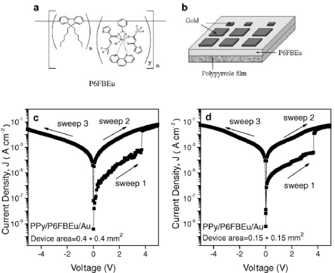
Systems with irreversible resistance switching represent a simple, non-volatile, WORM (write-once-read-many-times) memory. Very often, this type of memory is observed in organic devices Moller et al. (2003); Stewart et al. (2004); Choi et al. (2008b); Li et al. (2007). Figure 14 shows a schematic of irreversible switching loop when the device initially fabricated in the OFF state is switched into the ON state. This type of behavior is indeed observed experimentally Li et al. (2007). Figure 23 shows an example of characteristics of a flexible polymer device based on the conjugated copolymer 9,9-dihexylfluorene and benzoate with chelated europium thenoyltrifluoroacetone ligand complex (P6FBEu). This device shows an irreversible OFFON switching at a bias of V, ON/OFF current ratio of 200, and stability of the ON and OFF states up to reading cycles at 1V read voltage Li et al. (2007). The authors of this work have suggested a charge-migration mechanism to explain the hysteresis.
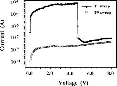
Moreover, the different direction of switching, when a device fabricated in ON state is switched into an OFF state is also possible Moller et al. (2003); Stewart et al. (2004); Choi et al. (2008b). For example, in figure 24 we report curves of indium-tin-oxide/hyperbranched copper phthalocyanine polymer/Ti (ITO/HCuPc/Ti) device Choi et al. (2008b). Such a device shows an irreversible ONOFF switching behavior at approximately 4.75V with a titanium top electrode, and at 2.5V with a gold electrode instead of Ti Choi et al. (2008b). Moreover, the authors of this work report a stability of ON- and OFF-states during , 1V amplitude read pulses, and a stability of both states after 1 year of storing. The switching into the OFF state is explained by rupture of filaments which takes place when a high voltage is applied Choi et al. (2008b). However, the origin of the filaments in a virgin device is not elucidated and more work in this direction is thus highly desirable.
III.2.4 Models of resistance switching devices
Several models of resistance switching have been proposed recently Baikalov et al. (2003); Rozenberg et al. (2004, 2005, 2006); Nian et al. (2007); Strukov et al. (2008, 2009); Pershin et al. (2009); Tamura et al. (2009); Joglekar and Wolf (2009); Jeong et al. (2009c); Shin et al. (2010) including molecular dynamics simulations Savel’ev et al. (2010). Some of them were implemented in SPICE (Simulation Program with Integrated Circuit Emphasis) Biolek et al. (2009a, b); Benderli and Wey (2009); Rak and Cserey (2010); Sharifi and Banadaki (2010); Zhang et al. (2010). Here, we consider several models of memristive devices Strukov et al. (2008); Joglekar and Wolf (2009); Pershin et al. (2009) that elucidate the resistance switching from the point of view of memristive theory Chua and Kang (1976).
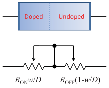
A simple model of titanium dioxide memristive system was suggested by Strukov and co-authors in their paper Strukov et al. (2008). In this work, a semiconductor film of thickness sandwiched between two metal electrodes is modeled using two variable resistors connected in series (see figure 25 (a)). These resistors represent two spatial regions with a high and low concentration of dopants. The application of the external bias causes charged dopants to drift thus moving the boundary between the regions. This process is described by the equations
| (63) | |||||
| (64) |
Here, denotes the ion mobility. Equation (64) gives
| (65) |
which, inserted into equation (63), in the limit of gives the memory resistance
| (66) |
The latter equation describes an ideal current-controlled memristor (see section II.4). We note, however, that the derivation of equation (66) is based on several assumptions such as current-controlled drift, constant mobility, and does not account for the boundary conditions. Many of these assumptions may in fact not hold in the actual experimental conditions. Moreover, experimentally observed curves actually correspond to a memristive system (in the sense of equations (27) and (26)) rather than to an ideal memristor. The model of Strukov and co-authors Strukov et al. (2008) was later improved by Joglekar and Wolf Joglekar and Wolf (2009) who introduced a function that ensures no drift at the boundaries. Their model is summarized in the table 5.
| Physical system | Solid state memristive device |
|---|---|
| Internal state variable(s) | Doped region size, |
| Mathematical description | |
| System type | First-order current-controlled memristive system |
Several later papers by the same group Strukov and Williams (2009a); Strukov et al. (2009); Pickett et al. (2009) report on further development of resistance switching theory for TiO2 devices. In reference Strukov and Williams (2009a) a model of threshold-type switching is suggested. Within this model the ion drift in a periodic potential is facilitated when the potential is significantly tilted by the applied electric field. Pickett et al. Pickett et al. (2009) have considered a model that involves an exponential dependence of the switching time on the device current. A coupled drift-diffusion equations approach to ionic and electronic transport was instead considered in reference Strukov et al. (2009).
We have recently introduced Pershin et al. (2009) a different model of memristive system that takes into account a threshold-type switching and boundary conditions (imposed on system’s memristance). The former is frequently observed in the bipolar resistance switching devices considered in section III.2.1. This model is based on the assumption that the rate of the resistance change is small below a threshold voltage and fast above , and was inspired by the experimental work of reference Strukov et al. (2008). The mathematical formulation of this model is provided in the table 6.
| Physical system | Solid state memristive device |
|---|---|
| Internal state variable(s) | Resistance, |
| Mathematical description | |
| System type | First-order voltage-controlled memristive system |
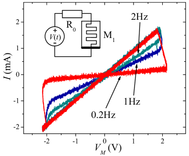
The model from table 6 was used to describe learning of simple biological organisms (see section VII.2.3) as well as in several other publications Pershin and Di Ventra (2010a, d, b). In figure 26 we demonstrate curves of a memristive system described by equations shown in the table 6 and obtained using a memristor emulator (see section VII.2.5). Note the similarity of these curves with those, for example, in figure 18.
III.3 Phase-change memory cells
Phase-change memory cells utilize phase-change materials that can exist in at least two different phases: amorphous and crystalline. These two different phases are characterized by distinctive physical properties such as resistivity, optical reflectivity, etc. The idea of phase-change memory (also known as PCM, PRAM, PCRAM, Ovonic Unified Memory, Chalcogenide RAM and C-RAM) relies on abilities to electrically induce switching between amorphous and crystalline states by the Joule heating due to the current flow and to probe the cell’s state by measuring its resistance. Since both states are stable, no energy is required to store data. Chalcogenides constitute most of the phase-change materials. They include Ge-Te Chen et al. (1986), GeSeTe2 H.B. et al. (2007), Ge2Sb2Te5 Senkader and Wright (2004), AgSbSe2 Wang et al. (2005), Sb-Se Yoon et al. (2006), Ag-In-Sb-Te Iwasaki et al. (1993). Here, we would like to focus only on memristive aspects of a phase-change memory cell that is a unit element of phase-change memory. Additional information about properties of phase-change materials and phase-change memory technology can be found in recent review papers Wuttig and Yamada (2007); Raoux et al. (2008); Raoux (2009).
(a)
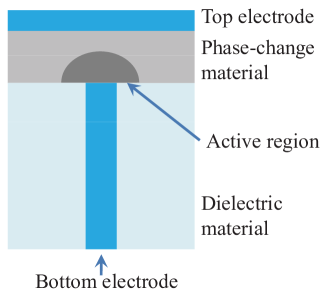 (b)
(b)
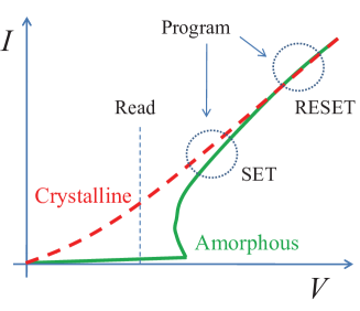
Fig. 27(a) shows schematically a so-called contact-minimized (”mushroom”) phase-change memory cell Raoux et al. (2008). It consists of a phase-change material sandwiched between large area (top) and small area (bottom) electrodes. The active (switchable) region of the phase-change material is located right above the bottom electrode where the current density is high. The cell design and operation regime normally do not allow the active region to contact the top electrode. Typical experimentally-measured curves Pirovano et al. (2004) of phase-change materials are shown schematically in Fig. 27(b). The switching from crystalline (low-resistive) to amorphous (high-resistive)) state (RESET operation) is performed by melting and quenching the material quickly enough. In this case, the material solidifies in the amorphous state. The switching from amorphous to crystalline state (SET operation) occurs when the material is heated above its crystallization temperature (which is below its melting temperature) for sufficiently long time. SET and RESET operations are achieved by unipolar pulses of appropriate amplitude and duration. Moreover, we note that the switching from amorphous (highly-resistive) to crystalline state would not be possible without a threshold-type increase of conductivity above a certain strength of the applied electric field (see Fig. 27(b)). Such an effect is not yet well understood and is currently related to the interplay between impact ionization and carrier recombination Raoux et al. (2008); Pirovano et al. (2004).
Theoretical and numerical modeling Pirovano et al. (2004); Kang et al. (2003); Ielmini and Zhang (2007); Kim et al. (2007b); Sonoda et al. (2008) of phase-change memory cells was previously reported focusing on either the total device operation or just some particular processes within a device (such as crystallization dynamics). In table 7 we summarize a memristive model of phase-change material cell based on the idea suggested by Sonoda and co-authors Sonoda et al. (2008). This model employs three rate equations to describe the following factors: temperature of active region, crystallization dynamics, and threshold behavior of conductivity of amorphous state. From the electrical point of view, the cell can be represented as three resistors , and connected in series Sonoda et al. (2008). Here, describes variable resistance of active region, while and the resistances below and above the active region, respectively (see figure 27(a)). In the table 7, we provide the memristive model with respect to the voltage drop on as in Ref. Sonoda et al. (2008). As the total cell consists of only resistive elements, it is memristive Chua and Kang (1976). We also note that phase-change memory cells have potential for multi-level applications Ovshinsky (2004); Ventrice et al. (2007); Yin et al. (2008); Lee et al. (2008).
| Physical system | Phase-change memory cell |
|---|---|
| Internal state variable(s) | Temperature, |
| Amorphous ratio, | |
| Switching variable, | |
| Mathematical description | |
| System type | Third-order voltage-controlled memristive system |
III.4 Metal-insulator phase transition memristive systems
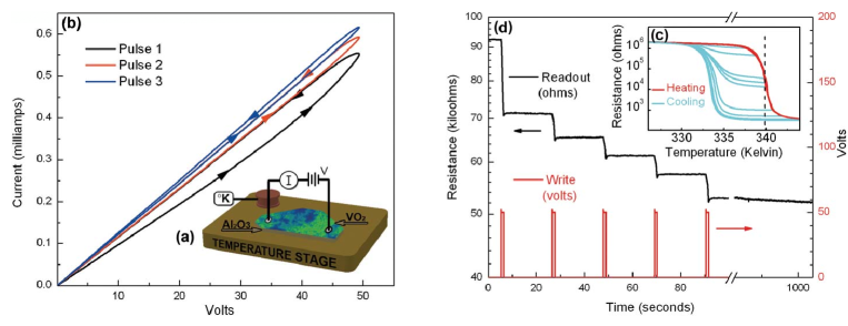
In strongly interacting electron materials, a complex interplay between charge, lattice and spin degrees of freedom can result in the resistance switching effect Quintero et al. (2007); Kim et al. (2006b). Driscoll and co-workers have recently used a vanadium dioxide based device to demonstrate memristive Driscoll et al. (2009a) and memcapacitive behavior Driscoll et al. (2009b) of systems comprising this oxide. In both types of experiments, the behavior is driven by the metal-insulator phase transition (MIT) of this material Morin (1959); Kim et al. (2006c, 2007a); Kübler et al. (2007); Arcangeletti et al. (2007); Qazilbash et al. (2006, 2008); Claassen et al. (2010). Here, we focus on the memristive behavior. The memcapacitive behavior of VO2 is discussed in section IV.3.2.
Using the experimental setup schematically shown in figure 28 where a film of VO2, deposited on a sapphire substrate, is connected to two electrodes, the memristive behavior was demonstrated as follows. The operation temperature was selected near the onset of the phase transition (340K) where VO2 properties are very sensitive to temperature changes. High amplitude voltage pulses (50V) were used to increase VO2 temperature for short periods of time thus promoting the MIT. Triggered by each pulse, nanoscale metallic regions develop within the insulating host, increasing in number and size to form a percolative transition Sharoni et al. (2008) (see figure 29 for an AFM image of these metallic regions).
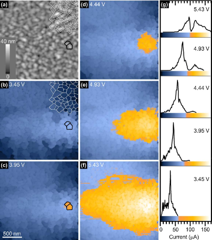
Figure 28(b,d) shows experimental results when ramping and step pulses are applied. The experimentally observed memristive properties of vanadium dioxide are related to power dissipated in VO2 Driscoll et al. (2009a). Therefore, in such a device and it can be classified as an even-function current-controlled memristive system. Consequently, the resistance rate of change does not depend on the applied signal polarity and can be switched only in one direction. Nonetheless, memory storage duration of more than several hours and the possibility to store up to resistance values in a single device have been reported Driscoll et al. (2009a), thus making this system a good model exhibiting multibit information storage.
We now introduce a mathematically-transparent model of vanadium dioxide memristive system. It can be developed assuming that the hysteresis in curves is well defined de Almeida et al. (2002); Ramírez et al. (2009); Lopez et al. (2002). This is a reasonable approximation taking into account that the resistance drift at a fixed temperature in the transition region is not very strong Claassen et al. (2010). The local temperature of the vanadium dioxide material can then be described by a heat transfer equation (similar to the heat equation of thermistor (32))
| (67) |
while the equation for the resistance dynamics can be written as
| (68) |
where is the heat capacitance, is the dissipation constant, is the temperature of the thermal stage, is the step function, and are ramp up and down curves, and is the resistance relaxation time that can be considered to be much shorter than characteristic thermal times. The first term on the right-hand side of equation (68) describes a resistance decrease when temperature increases, and the second term is responsible for the opposite process. As the resistance relaxation time is short, equation (68) represents very fast transition if and if . It is clear that, according to equation (68), does not change if its value falls inside of the hysteresis loop.
Thus, our description of MIT in VO2 involves two state variables, the temperature and resistance. The time dependence of state variables is given by equations (67,68). Since the current enters into the right-hand-side of equation (67), our model describes a second-order current controlled memristive system.
The experimentally measured profile of the hysteresis Driscoll et al. (2009b, a) suggests that the functions and can be selected of the same shape displaced by , where is the hysteresis width. For example, in our numerical simulations of memristive properties of vanadium dioxide shown in figure 30 we have employed the following profile for and
| (69) | |||||
| (70) | |||||
| (71) |
where and are asymptotic values of resistance below and above the transition temperature, respectively, is the average transition temperature and is the parameter defining the sharpness of the resistance step at the metal-to-insulator transition. An example of a hysteresis loop based on equations (69-71) is demonstrated in Figure 30(a). We emphasize that the choice of and given by equations (69-71) is not unique and possibly better fits to experimental curves can be found.
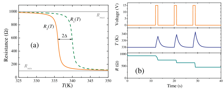
| Physical system | Vanadium dioxide memristive device |
|---|---|
| Internal state variable(s) | Temperature and resistance, , |
| Mathematical description | |
| System type | Second-order current-controlled memristive system |
The application of voltage pulses to vanadium dioxide memristive system results in a local heating as demonstrated in figure 30(b). Since the resistance of the system decreases with each pulse, the amount of heat released due to subsequent pulses increases. This can be clearly seen in the increasing pulses’ magnitude in the curve. This mechanism permits the progress of the insulator-to-metal transition using pulses of fixed amplitude and width. The resulting steps shown in figure 30(b) are similar to those observed experimentally Driscoll et al. (2009a) (compare with figure 28).
The reversible resistance switching was recently observed in a manganite La0.225Pr0.4Ca0.375MnO3 at low temperatures Yan et al. (2009). In this material, the resistance switching effect is explained by a Joule heat-induced transition between charge-ordered insulator and ferromagnetic metal phases Yan et al. (2009). The authors show that such a transition is bidirectional and can be uniquely controlled by current pulse pairs Yan et al. (2009). Below 30K, the system enters into a frozen state in which the phase separation is blocked. Under this condition, low and high resistance states become nonvolatile. Figure 31 demonstrates that the resistance switching in La0.225Pr0.4Ca0.375MnO3 has a pronounced frequency dependence. This feature is typical for memristive systems and can be potentially used for multi-state memory. However, we emphasize that the hysteresis in this particular material is not suitable for room-temperature applications.
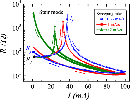
III.5 Spintronic systems
Memory is not necessarily confined to structural or charge properties but may also arise from the spin degree of freedom. This is a particularly important result in view of the possible development of devices that operate with low dissipation and show high reliability under ac-bias conditions. In the following, we then discuss memory effects in the two major areas of spintronic research: semiconductor Zutic et al. (2004) and metal Bratkovsky (2008); Brataas et al. (2006) spintronics.
III.5.1 Semiconductor spintronic systems
It was shown by Pershin and Di Ventra Pershin and Di Ventra (2008b) that memory effects are an intrinsic feature of many semiconductor spintronic systems. These effects have a spin-related origin and, consequently, can not be observed in spin unpolarized systems. The general idea behind these memory phenomena is as follows. If we consider a structure (such as, for example, a semiconductor/ferromagnet junction) driven by a time-dependent external control parameter (such as applied voltage or current) then, when the external control parameter changes, it takes some time for the electron spin polarization to adjust to a new control parameter value - typically, the equilibration is governed by electron-spin diffusion and relaxation processes Pershin and Di Ventra (2008b). Within the time scale of this “spin-polarization adjustment”, the system keeps its memory on the past dynamics and, when, in addition, the level of electron spin polarization influences the system’s resistance, it exhibits memristive behavior.
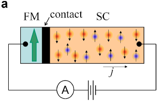
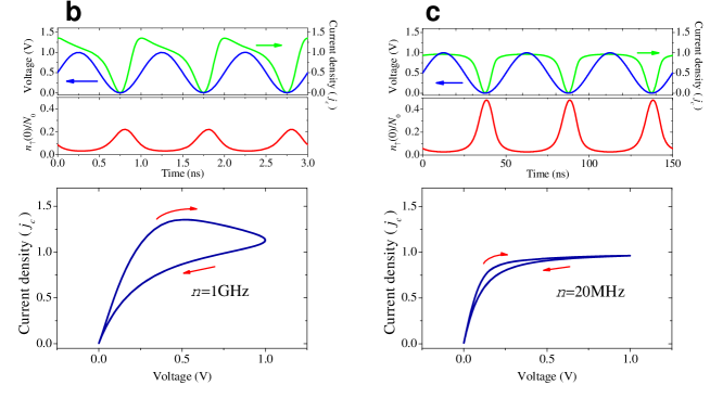
As an example, let us consider current flowing through a semiconductor-half-metal (namely, a perfect ferromagnet Attema et al. (2006)) junction (see figure 32(a)) in such a way that the electron flow is directed from the semiconductor into the ferromagnet (this process is called spin extraction). It is known that spin extraction is accompanied by the phenomenon of spin blockade Pershin and Di Ventra (2007) characterized by a saturated curve Pershin and Di Ventra (2008a). Physically, the outflow of majority-spin electrons from the semiconductor leaves a cloud of minority-spin electrons near the junction. This minority-spin cloud can limit the majority-spin current creating a pronounced spin-blockade at a critical current density Pershin and Di Ventra (2007)
| (72) |
where is the electron density in the semiconductor, is the diffusion coefficient, and is the spin-relaxation time.
The time evolution of the electron spin polarization in a non-degenerate semiconductor can be described by the two-component drift-diffusion model Yu and Flatté (2002)
| (73) |
| (74) |
which are accompanied by an equation for the total voltage drop Pershin and Di Ventra (2007)
| (75) |
where is the electron charge, is the density of spin-up (spin-down) electrons, is the corresponding current density, is the conductivity, is the mobility, is the length of the semiconductor region, is the electric field, is the semiconductor resistivity, and is the contact resistivity at .
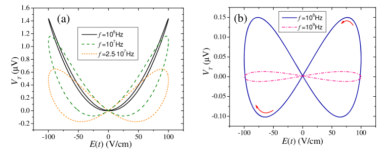
Clearly, equations (73,75) define a continuous current-controlled memristive system (note that by inverting equation (75) it can also be redefined as a voltage-controlled memristive system). In such a system, the majority-spin density at the boundary defines (through equation (75)) the resistance of the device. The details of the memristive model of semiconductor/half metal junctions (in the assumption of constant electron density) is summarized in the table 9. The differential equation for the continuous state variable ( is the direction perpendicular to the interface) should be solved with the boundary conditions specified in the caption of table 9. In figure 32(b,c) we show a numerical solution of the above equations with appropriate boundary conditions Pershin and Di Ventra (2008b). The pinched hysteresis loops demonstrate typical frequency behavior for memristive systems.
| Physical system | Semiconductor/half-metal junction |
|---|---|
| Internal state variable(s) | Density of spin-up electrons, |
| Mathematical description | |
| System type | Continuous current-controlled memristive system |
In addition to the above results, in certain semiconductor spintronic systems, spin memory effects can be observed directly in the transverse voltage. For example, this occurs in spin Hall effect systems Dyakonov and Perel (1971); Wunderlich et al. (2005) with an inhomogeneous electron density in the direction perpendicular to the direction of main current flow Pershin and Di Ventra (2009). Figure 33 shows transverse voltage hysteresis loops that demonstrate typical memristive behavior: non-linear dependence at low frequencies, pronounced hysteresis at higher frequencies, and hysteresis collapse at very high frequencies Pershin and Di Ventra (2009). The physical origin of this effect is similar to what we have discussed above: the time it takes for the electron spin polarization to relax to its instantaneous equilibrium configuration is finite, thus leading to a history-dependent observable.
III.5.2 Metal spintronic systems
A different class of spin-based memristive systems takes advantage of all-metal spintronic devices Bratkovsky (2008); Brataas et al. (2006). The operation of such devices can employ spin-torque-induced magnetization switching or magnetic-domain-wall motion Wang et al. (2009). Figure 34 depicts both schemes.
Spin-torque transfer systems - One realization (figure 34(a)) is based on spin-torque transfer Berger (1978); Slonczewski (1996); Tsoi et al. (1998); Myers et al. (1999). In spin-torque transfer systems, the resistance is determined by the relative magnetization between opposite sides of a magnetic tunnel junction. Current flowing through the junction induces spin torque, in turn changing the relative magnetization.

Quite generally, considering injection of spin-polarized electrons from a reference layer (with a fixed direction of magnetization) into a free layer (whose magnetization direction can change), the magnetization dynamics of the free layer can be described by the Landau-Lifshitz-Gilbert equation Landau and Lifshitz (1935); Gilbert (1955); Slonczewski (1996). Parameterizing the magnetization direction of the free layer by two angles and (according to Sun (2000), is the angle between the magnetization direction and a uniaxial anisotropy axis assumed to be in the interface plane, and is the angle in the plane perpendicular to the uniaxial anisotropy axis) the Landau-Lifshitz-Gilbert equation can be written as Sun (2000)
| (76) |
where the functions and on the right hand side take into account different factors influencing magnetization dynamics such as uniaxial anisotropy, easy-plane anisotropy, magnetic field, spin-torque and dissipation Sun (2000). The resistance of the magnetic tunnel junction is determined by the angle between magnetization directions of the free and reference layer that can be expressed using and . Consequently, from the point of view of memory systems, the magnetic tunnel junctions can be categorized as second-order current-controlled memristive systems.
To illustrate the origin of memory behind these concepts, let us consider a simple system of a free layer with uniaxial anisotropy only. In this case, the Landau-Lifshitz-Gilbert equation involves only and the order of the memristive system is reduced. For this specific situation, equations (76) are written as Wang et al. (2009); Sun (2000)
| (77) |
where is the angle between the free-layer magnetization direction and the pinned-layer (reference layer) magnetization direction, is the gyromagnetic ratio, is the damping parameter, is the perpendicular anisotropy of the free layer, and describes the effect of the polarized-current () spin-torque. Here, is the polarization efficiency, is the film-element volume and is the magnetization saturation.
Resistance of the corresponding magnetic tunnel junction (MTJ) is given by
| (78) |
where is the MTJ conductance when , and the tunneling magnetoresistance, , is the ratio of the difference between high and low conductance to low conductance (high conductance occurs when both layers magnetizations are parallel to each other and low conductance when the magnetizations are antiparallel). The model of spin-torque transfer device discussed above is condensed in the table 10. Its memristive origin is evident. In fact, an interesting feature of this system is the periodicity of the angle when it is changed by . The state variable , actually, can not record such a change. This feature should be taken into account in studies of such structures.
| Physical system | Spin torque transfer device |
|---|---|
| Internal state variable(s) | Magnetization direction angle, |
| Mathematical description | |
| System type | First-order current-controlled memristive system |
Spin-torque-induced domain-wall motion - In the second realization of metallic spintronics (figure 34(b)) a long spin-valve structure is realized with domain-wall motion in the free layer induced by the current Wang et al. (2009). In this geometry, the current flows in both free and reference layers. The resistance of such a structure depends on the domain-wall position (along the direction of current flow) as
| (79) |
Here, is the free-layer length, is the low resistance when magnetizations of free and reference layers are parallel and is the high resistance when magnetizations of both layers are antiparallel. In a linear approximation, the domain wall velocity is proportional to the current strength
| (80) |
where is a proportionality coefficient. Equation (80) should be solved with the boundary conditions . It follows from equations (79,80) that the device is described by general equations
| (81) |
Therefore, this spin-valve structure with domain-wall motion is also a first-order current-controlled memristive system. When the position of the domain wall is confined inside the free layer (), we can integrate equation (80) obtaining . In this regime, the device behaves as an ideal memristor whose memristance is given by
| (82) |
In reality, the domain wall motion is a complex process. Consequently, equation (82) provides only a first approximation Wang et al. (2009) to the device response.
| Physical system | Domain wall |
|---|---|
| Internal state variable(s) | Position, |
| Mathematical description | |
| System type | Current-controlled memristor |
Wang et al. have suggested to use the temperature dependence of the domain wall mobility - which is observed within a certain range of parameters - to sense an external temperature Wang et al. (2010b). Generally, the domain wall velocity as a function of the driving current has a threshold-type dependence Zapperi et al. (1998). Around the critical current value, the thermal fluctuations play an important role in the domain wall de-pinning from crystallographic defects thus providing a basis for thermal sensitivity Wang et al. (2010b). The resulting spintronic memristor temperature sensor has the same device structure as shown in figure 34(b). For temperature sensing, it is suggested to apply a voltage pulse of a constant magnitude to the device. The resistance difference before and after the voltage pulse is measured and calibrated to sense the temperature. Theoretically, the domain wall motion in the critical current region is described by stochastic differential equations Duine et al. (2007). Therefore, this system is an example of a stochastic memory circuit element introduced in section II.1.
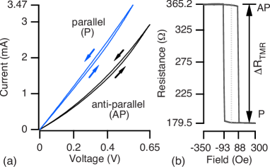
A different approach to memristive switching of magnetic junctions was followed by Krzysteczko et al. Krzysteczko et al. (2009). These authors have fabricated a MgO modified magnetic tunnel junction with a resistive switching material inside. As shown in figure 35, resistive switching results in a splitting of magnetoresistance curves. The authors observed a tunnel magnetoresistance of about 100% ratio, and bipolar resistive switching of about 6%. Five resistance states were demonstrated. This approach is thus a promising alternative to create multi-bit states for storage and logic.
III.6 Ionic channels
Another important memristive system pertains to biological neural networks, and in particular to the functioning of membranes in axon cells. In fact, in 1952 Hodgkin and Huxley suggested a model of action potentials Hodgkin and Huxley (1952) in neurons that employs history-dependent channel conductances that are essentially memristive. This model is one of the most significant conceptual achievements in neuroscience Wang et al. (2000). In its original formulation, the nerve membrane (specifically, the membrane of the squid giant axon) was described by three types of ion channels: leakage channels (primarily carrying chloride ions), Na channels and K channels. Leakage channels are mainly responsible for the resting membrane potential and have a relatively low constant conductance. The conductance of the other two channels changes as a function of time and voltage, and here lies the memristive behavior we are interested in. Hodgkin and Huxley have demonstrated that step depolarizations of the squid axon trigger a rapid inward current across the membrane carried by Na+ ions, followed by an outward current due K+ ions.
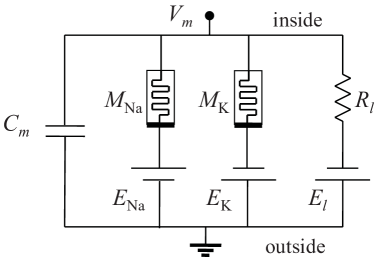
In order to quantitatively understand the experimental data, they have then suggested an equivalent circuit model of the membrane as shown in figure 36. In this plot, we use symbols of memristors in order to denote variable conductance channels. Mathematically, the membrane current is written as Hodgkin and Huxley (1952)
| (83) |
where the memory conductances , , with , , constants, describes the leakage resistance, and all other circuit quantities can be read from the circuit diagram 36. The time-dependencies of voltage-dependent gating variables , and are given by the equations
| (84) | |||
| (85) | |||
| (86) |
where and are voltage-dependent constants Hodgkin and Huxley (1952) defined as
| (87) | |||
| (88) | |||
| (89) | |||
| (90) | |||
| (91) | |||
| (92) |
In the above equations, the voltage is in mV and time is in ms. The quantities , and take values between 0 and 1 thus representing variation of channels’ conductances in time.
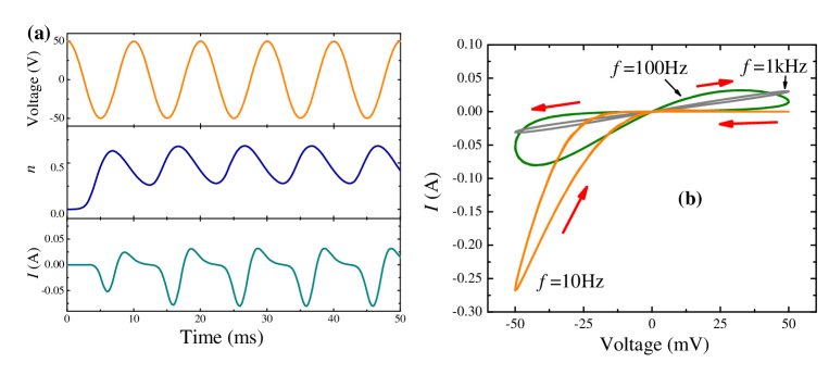
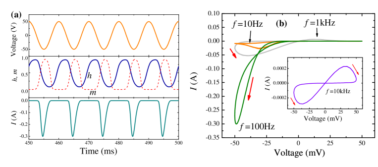
It follows from the expressions for and (given below equation (83)) and equations (84-86) that the potassium channels can be classified as first-order voltage-controlled memristive systems and the sodium channels as second-order voltage-controlled memristive systems Chua and Kang (1976). In figures 37, 38 we plot simulations of potassium and sodium channel memristive systems biased by ac-voltage. These plots demonstrate frequency-dependent curves typical of memristive systems. There is, however, an interesting feature that can be seen in figure 38(b) for the Hz curve: at negative voltages, the curve has a self-crossing. To the best of our knowledge we are not aware of experimental results for these systems that employ ac biases, and thus this self-crossing feature remains to be verified.
Modern models of neuronal dynamics are based on similar equations, but often involve many more ion channel types, with the ion channels possibly located on different parts of a spatially extended neuron Moss and Gelen (2001). Therefore, a single neuron description may involve a large number of memristive systems.
IV Memcapacitive systems
Having discussed experimental realizations of memristive systems, in this section we consider systems showing memcapacitive behavior. Under the term capacitor, we understand a general electronic device capable of storing charge and energy. Such a device normally includes a couple of external metal plates having negligible resistance and a dielectric medium between the plates. In capacitors, memory effects can originate from changes in the geometry and/or permittivity (figure 39).
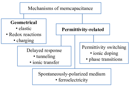
Under geometrical mechanisms of memcapacitance we understand situations when geometrical morphology of the plates changes in time (e.g., their relative distance and/or shape). In permittivity-related mechanisms, dielectric properties of the material between the plates provide the memory. We can identify three most probable permittivity-related mechanisms (figure 39): delayed-response mechanism, when dielectric permittivity dynamics involves a time delay, permittivity-switching mechanism, when the dielectric constant changes its value under the external input (but the response is fast), and spontaneously-polarized medium mechanism, in which a spontaneously-polarized material (ferroelectric) is used in the capacitor structure.
We discuss below physical systems demonstrating these different mechanisms of memcapacitance. Known mathematical models of some of these systems are also presented. We also note that a methodology for SPICE modeling of memcapacitive systems has been developed recently Biolek et al. (2010b).
IV.1 Geometrical memcapacitive systems
IV.1.1 Micro- and nano-electro-mechanical systems
Micro-electro-mechanical system (MEMS) and nano-electro-mechanical system (NEMS) capacitors Rebeiz (2002); Varadan et al. (2002); Evoy et al. (2004); Luo et al. (2006); Jang et al. (2008); Herfst et al. (2008); Nieminen et al. (2002) are variable capacitors whose operation is based on an interplay of mechanical and electrical properties of micro- and nano-size systems. Such elements are key components in many radio-frequency (RF) applications such as tunable filters, impedance matching circuits and voltage-controlled oscillators Rebeiz (2002); Varadan et al. (2002). In addition, these structures, on the nanoscale, are considered for memory applications Jang et al. (2008) and sensitive measurements LaHaye et al. (2009). Normally, capacitors built from these systems utilize a diaphragm-based, a microbridge-based or a cantilever-based structure fabricated via micromachining Rebeiz (2002); Varadan et al. (2002).
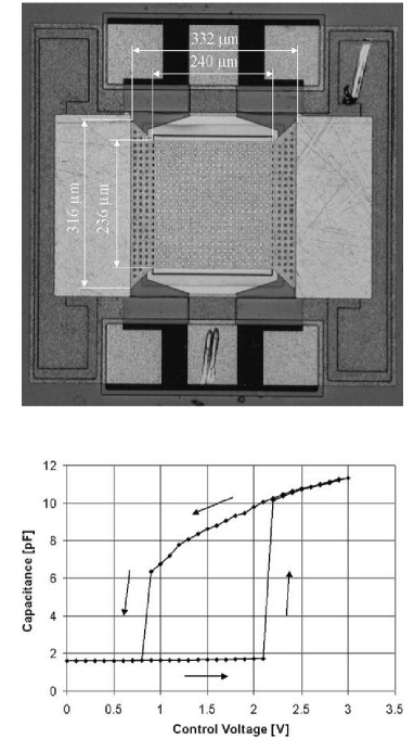
Figure 40 shows an experimental image of a memcapacitive system constructed from MEMS and measured capacitance as a function of voltage. The capacitance curve shows a well defined hysteresis which is a manifestation of memory effects in the structure. Memory effects are related to displacement of a top capacitor plate that can be considered to be suspended by a spring Nieminen et al. (2002). Below, we consider a model of elastic memcapacitive system that (with appropriate boundary conditions) can be used to described the capacitor features of the MEM system shown in figure 40. For more details on MEMS and NEMS we refer to Rebeiz (2002); Varadan et al. (2002); Pelesko and Bernstein (2002).
IV.1.2 Elastic memcapacitive systems
A model of a simple elastic memcapacitive system is discussed in Sec. II.5.3 of this review. Here, we would like to mention about a different elasticity-based memcapacitive system Martinez-Rincon and Pershin (2010) whose schematics is shown in Fig. 41. In this realization, the capacitor is formed by a strained membrane (upper plate) and a flat fixed lower plate. In this model two equilibrium states (up-bent and down-bent membrane) coexist that can be used for a non-volatile storage of a bit of information. The possibility of switching between the two states as well as chaotic behavior of such a system in a certain range of parameters has also been demonstrated Martinez-Rincon and Pershin (2010). For reference, we provide the model of strained membrane memcapacitive system in the table 12.
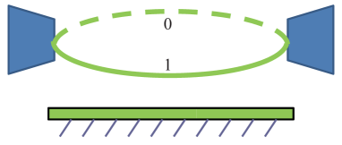
| Physical system | Strained membrane memcapacitive system |
|---|---|
| Internal state variable(s) | Displacement and velocity of upper plate, |
| , | |
| Mathematical description | |
| System type | Second-order charge-controlled memcapacitive system |
IV.1.3 Other geometrical memcapacitive systems
There are other possible realizations of geometrical memcapacitive systems. In many memristive systems, for example, the morphology of conducting regions changes in time Waser and Aono (2007). Therefore, in addition to a resistance change, the capacitance of such systems changes as well. In particular, co-existence of memristive and memcapacitive behavior has also been observed in perovskite thin films Liu et al. (2006) (see also figure 10).
IV.2 Delayed-response memcapacitive systems
IV.2.1 Superlattice memcapacitive systems
A solid-state memcapacitive system based on the slow polarization rate of a medium between plates of a regular parallel-plate capacitor has been recently proposed Martinez-Rincon et al. (2010). The key idea is to use non-linear electron transport (tunneling) for fast writing and long storage capabilities. Figure 42(a) shows a particular example of memcapacitive system in which metal layers are embedded into an insulating material between external capacitor plates. The structure is designed in such a way that the electron transport between external plates and internal layers is not possible. Therefore, the internal charges can only be redistributed between the internal layers creating a medium polarization. Correspondingly, there is a constrain imposed on the total internal charge:
| (93) |
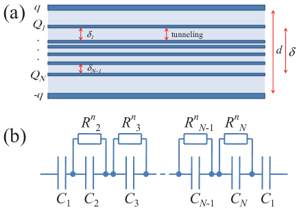
The capacitance of the total structure is given by Martinez-Rincon et al. (2010)
| (94) |
where , are geometry-related parameters. The dynamics of the charge at a metal layer is determined by the currents flowing to and from that layer:
| (95) |
where is the tunneling electron current flowing from layer to layer (for more details see reference Martinez-Rincon et al. (2010)). It follows from equations (93,94,95) that such a superlattice memcapacitive system is an order charge-controlled memcapacitive system. Table 13 presents summary of the superlattice memcapacitive system.
| Physical system | Superlattice memcapacitive system |
|---|---|
| Internal state variable(s) | Charges on internal metal plates, |
| () | |
| Mathematical description | |
| System type | ()-order charge-controlled memcapacitive system |
Simulations of a two-layer memcapacitive system with symmetrically positioned internal layers is depicted in figure 43. Interesting features of this memcapacitive system include non-pinched hysteresis loop (figure 43(c)), and both negative and diverging capacitance (figure 43(d)). Moreover, since electron tunneling between the layers is accompanied by energy loss, the memcapacitive system is dissipative (figure 43(e)). Using a set of non-linear resistors and usual capacitors, an equivalent model of the given memcapacitive system can be formulated (see figure 42(b)). This is an example of the situation - anticipated in section II.8 - in which a memcapacitive system can be constructed from classical circuit elements. We re-iterate here that this is not a trivial point because one can use a unified set of equations, (4) and (5), describing a single memory system to represent a complex functionality as that reported here.
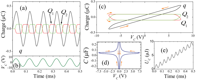
IV.2.2 Ionic memcapacitive systems
Memcapacitive behavior can be observed also in certain ionic systems because of their relatively slow dielectric response. A typical nanopore sequencing setup Branton et al. (2008); Zwolak and Di Ventra (2008) is an example of such a system. Let us then consider two chambers with ionic solution separated by a membrane with a nanopore Krems et al. (2010). When a varying voltage is applied to electrodes located in different chambers, ions redistribute with a time lag affecting the total system capacitance. In particular, it has been shown Krems et al. (2010) that the ac response of such a system demonstrates non-pinched hysteresis loops, and both negative and divergent capacitance. Moreover, the equivalent scheme of this setup can also be modeled using a set of classical circuit elements Krems et al. (2010). Since nanopores are ubiquitous on membranes of biological cells (e.g., the nerve cells) we expect these phenomena to be observable (at appropriate frequencies) even in those cases. We are not aware, though, of either theoretical or experimental work along these lines.
IV.3 Permittivity-switching memcapacitive systems
IV.3.1 Polymer-based memcapacitive systems
An analog memory capacitor has been reported in reference Lai et al. (2009). In this work the programmable capacitance was achieved in a field-configurable doped polymer, in which the modification of ionic concentrations induces a nonvolatile change in the polymer dielectric properties. Several device structures were investigated and two of them are shown in figure 44. In both structures, the RbAg4I5 ionic conductor functions as an ionic source. It contains Ag cations having a higher mobility and iodine anions whose mobility is lower and, in a polymer, is of a threshold type. The latter is because the iodine anions, having a much larger radius, can form a large ionic complex I, and/or chemically bond with the MEH-PPV polymer used in the memory capacitor.
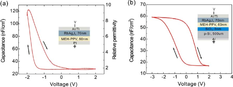
Negative voltage pulses above a threshold were used to inject iodine anions into the polymer, while positive voltage pulses (above the threshold) were used to extract iodine anions from the polymer. Some of Ag cations follow the iodine anions because of electrostatic interactions. When in the polymer, the anions and the cations form ionic dipoles increasing the polymer permittivity and device capacitance Lai et al. (2009). Since a voltage above a threshold is needed to overcome the ionic bonding with the polymer, the devices provide reasonably nonvolatile memory characteristics Lai et al. (2009). In particular, it has been reported that after the analog capacitance was configured to a certain value, it changed by less then 10 under continuous reading for 5 days.
IV.3.2 Phase-transition memcapacitive systems
During the process of a metal-to-insulator transition (MIT) both resistance (as we discussed in section III.4) and dielectric properties Qazilbash et al. (2007); Driscoll et al. (2008) are affected. This latter property was used to fabricate a memory metamaterial in which a persistent electrical tuning of a resonant frequency was demonstrated Driscoll et al. (2009b). In this particular case, vanadium dioxide has been used as the memory material undergoing the MIT, which we have discussed in section III.4 in the context of memory resistance. In the experimental setup, a split-ring resonator array was patterned on a 90-nm thin film of vanadium dioxide connected by two electrodes to a voltage source. The device was mounted on a temperature-controlled stage and a temperature of 338.6 K was selected. At this temperature, the slope of the resistance as the function of temperature is the steepest because of the proximity to the MIT. Therefore, even small amplitude voltage pulses have a notable effect on material characteristics Driscoll et al. (2009b). Such electrical pulses directly applied to vanadium dioxide were used to modify its dielectric properties. The latter ones were registered by measuring the modification of the resonant frequency of the split-ring resonator array.
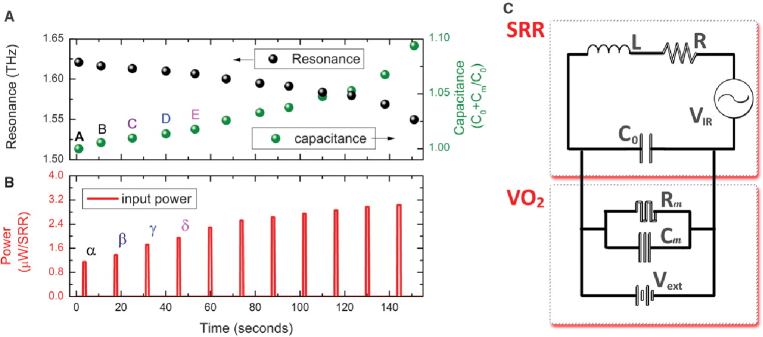
Figure 45(a) demonstrates the experimentally measured increase in the metamaterial capacitance with each applied voltage pulse. As the input power per pulse increases with pulse number (see figure 45(b)), the MIT in vanadium dioxide progresses causing the permittivity increase. Overall, the resonant frequency can be red-shifted by as much as 20% from its spectral maximum at THz Driscoll et al. (2009b). It is also worth noting that the effective circuit model of split-ring resonator deposited on vanadium dioxide involves both memristive and memcapacitive elements (figure 45). As already anticipated, memristive and memcapacitive properties co-exist very often, and in the metamaterial configuration Driscoll et al. (2009b) they play together an important role in the device operation.
IV.4 Spontaneously-polarized medium memcapacitive systems
IV.4.1 Ferroelectric memcapacitive systems
Another interesting concept is the use of ferroelectric materials Valasek (1921); Dawber et al. (2005); Lang (2006) as the dielectric medium of a memory capacitor. Ferroelectric materials are composed of domains with a non-zero average electrical polarization. The polarization of ferroelectric materials shows hysteresis as a function of electric field, revealing two well-defined polarization states. These states are used in the ferroelectric random-access memory (RAM) technology Scott and Paz de Araujo (1989) having functionality similar to Flash memory.
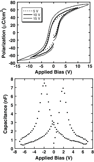
Experimentally, when ferroelectric materials are inserted into capacitor structures, a hysteretic behavior is observed (see, for example, references Kholkin et al. (2002); Kim et al. (2007c); Cagin et al. (2007); Ducharne et al. (2007)). In particular, in figure 46 we plot the polarization-voltage and capacitance-voltage characteristics of metal-ferroelectric-metal capacitor Pt/PZT/Pt where PZT is (Pb,Zr)TiO3 Cagin et al. (2007). In this plot, the curve demonstrates the characteristic “butterfly” shape related to ferroelectric material and can be thus characterized as a type-II memcapacitive system (cf. figure 2). In this experiment, the dielectric constant of the PZT film ranged from to , where is the vacuum permittivity. The peak capacitance occurring at V corresponds to the coercive field of the ferroelectric material.
IV.5 Other memcapacitive systems
IV.5.1 MOS capacitors with nanocrystals
Metal-Oxide-Semiconductor (MOS) structures with embedded nanocrystals (figure 47(a)) have been much investigated recently Kobayashi et al. (1997); Shi et al. (1998); Dimitrakis et al. (2003); Kim et al. (2001); King et al. (2001); Kim et al. (2002); Wang et al. (2004b, a); Su et al. (2005); Kanoun et al. (2006); Lee et al. (2006); Zhu et al. (2007); Choi et al. (2008a); Li and Liu (2010). These devices are promising candidates to replace floating-gate Flash memory. The latter, in fact, has long programming times and poor endurance. Many different materials such as Si Tiwari et al. (1996); Shi et al. (1998); Dimitrakis et al. (2003); Kim et al. (2001); King et al. (2001); Su et al. (2005), Ge Kobayashi et al. (1997); Kim et al. (2001, 2002); Wang et al. (2004b); Kanoun et al. (2006); Lee et al. (2006), SiGe Zhu et al. (2007); Li and Liu (2010), Au Paul et al. (2003) and Ag Wang et al. (2004a) have been considered as candidates for the nanocrystals that store charge. Currently, Ge nanoscrystals seem to be the most promising ones because of a better data retention due to the smaller band-gap compared to Si Lee et al. (2006).
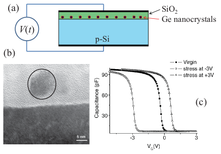
It is known that curves of usual MOS capacitors demonstrate a non-linear behavior Nicollian and Brews (2002) (see the ”Virgin” line in figure 47(c)). Nanocrystals added to a MOS structure (an actual Ge nanocrystal image is shown in figure 47(b)), provide a mechanism controlling the displacement of the curve. When charge is transferred to nanocrystals, the curve shifts by the amount determined according to the equation Kanoun et al. (2006); Tiwari et al. (1996)
| (96) |
where is the elementary charge, is the number of charges per nanocrystal, is the density of Ge nanocrystals, is the control oxide thickness, is the mean diameter of Ge nanocrystals, and are dielectric permittivities of Ge nanocrystals and oxide, respectively. Figure 47(c) demonstrates displacement of curves induced by positive and negative stress biases.
From the point of view of memory elements, the amount of transferred charge plays the role of the state variable defining the capacitance . The dynamics of can be described by a rate equation. However, the total equivalent scheme of such device should include a resistor in series with a capacitor as charge transfer to nanocrystals involves also dissipation processes. Indeed, such an equivalent resistor-capacitor circuit of MOS capacitors with nanocrystals was recently discussed Kwok (2008). Therefore, MOS capacitors with nanocrystals do not manifest a purely memcapacitive behavior, although the memcapacitive component in these devices seems to be the dominant one. This is thus an example of a combined system as those discussed in section II.7.
V Meminductive systems
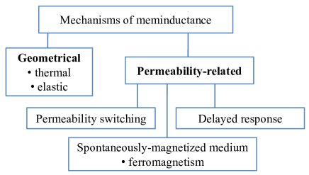
We are now left to consider systems that show meminductive behavior. These are systems whose inductance depends on the past dynamics and which can store energy. In this case, the energy stored may be a combination of magnetic energy and energy due to other degrees of freedom (e.g., elastic kinetic energy). Similar to the case of memcapacitive systems, memory effects in inductors can originate from a geometrical variation of their structure, or be related to their permeability (see figure 48). Although at the present time meminductors and meminductive systems are the least studied members of the family of circuit elements with memory, there are nonetheless several interesting examples of such devices, and owing to their practical importance, we expect more will be discovered/designed in the future. Moreover, several SPICE models of meminductive systems have been suggested Biolek et al. (2010a). Below, we overview experimental realizations of meminductive systems based on the bimorph effect, introduce a model of an elastic meminductive system, and discuss some other possible realizations of these elements.
V.1 Geometrical meminductive systems
V.1.1 Bimorph meminductive systems
Like for memcapacitive systems’ realizations, the micro-electro-mechanical system (MEMS) technology provides an opportunity to fabricate devices whose operation is based on an interplay of mechanical, electrical, magnetic and thermal properties. Several designs of inductors based on tunable MEMS that employ the bimorph effect Chu et al. (1993) have been reported Lubecke et al. (2001); Zine-El-Abidine et al. (2004); Chang and Sivoththaman (2006). The bimorph effect refers to composite materials that show electrothermal actuation, namely they show reversible mechanical deformation under electrothermal effects. The tunability of the inductors based on this effect is then achieved by the difference in thermal expansion coefficients of the two materials forming the inductor. When a voltage is applied to such a structure, its temperature changes due to heating and the structure deforms in a controllable manner. As a finite time is required for heating and cooling, the inductance is history-dependent. Therefore, such a device behaves as a meminductive system.
(a)
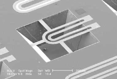 (b)
(b)
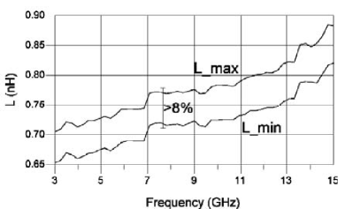
(a)
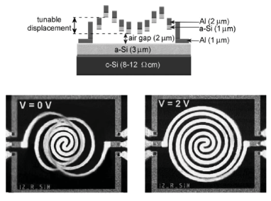 (b)
(b)
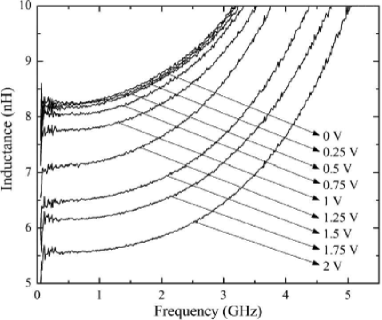
Two experimental designs of bimorph-effect based meminductive system are shown in figure 49(a) and figure 50(a). The first structure (figure 49(a)) consists of two inductors (fabricated of gold/silicon nitride bi-layer) connected in parallel. The outer loop inductor is fixed by nitride beams while the inner inductor is free to move. The heating of the structure by current causes the inner inductor to deflect downwards changing the structure’s inductance. A variation of the inductance as much as 8% was reported Zine-El-Abidine et al. (2004). A larger tuning range of 32% is achieved in the structure shown in Figure 50(a). Here, the meminductive system is made of an amorphous-silicon/aluminum (a-Si/Al) coil. Figure 50(a) shows that an applied dc voltage flattens the initial 3D structure.
The modeling of such meminductive systems should be based on the heat transfer equation, similar to the case of thermistors (see section III.1). In the simplest case, we can assume that the device state is defined by a single temperature , that is,
| (97) |
where is the magnetic flux piercing the inductor, is the current that flows in it, and satisfies
| (98) |
where is the heat capacitance, is the dissipation constant of the device, and is the background (environment) temperature. It follows from equations (97,98) that meminductive systems based on the bimorph effect are first-order current-controlled meminductive systems. Moreover, since the state function (equation (98)) and the response function (equation (97)) are even functions of the current, these systems (under these simplified assumptions) should exhibit type-II hysteresis loops under a periodic stimulus (see figure 2). Table 14 summarizes properties of bimorph meminductive systems.
| Physical system | Bimorph meminductive system |
|---|---|
| Internal state variable(s) | Temperature, |
| Mathematical description | |
| System type | First-order current-controlled meminductive system |
V.1.2 Elastic meminductive system
A model of meminductive system whose operation is based on an interplay of elastic forces with current-current interaction can be found in Sec. II.6.3 of this review.
V.2 Other meminductive systems
Having discussed geometry-based meminductive systems, we now turn to other possible realizations that, as it was mentioned above, can be based on peculiarities in the permeability response. In particular, a meminductive behavior can be realized using the core material whose response to the applied magnetic field depends on its history. As an example, we can think about ferromagnetic materials exhibiting a magnetic hysteresis such as iron or iron-based alloys. Such inductors can be easily realized in practice, and the desired orientation of the ferromagnetic core easy axis with respect to the coil direction can be selected Vroubel et al. (2004). Moreover, a mathematical framework to model iron-core inductors is reported in Matsuo et al. (1999). As of now, however, a clear connection of such inductors with the theory of memory elements has not been developed. In addition, memory effects in inductance (such as lagging) were revealed in the context of superconducting circuits Shevchenko et al. (2008). An interesting - yet unexplored - direction is to employ field-induced ion motion in solid state electrolytes for non-volatile realizations of meminductive systems.
VI Other systems with memory
In this section we consider several systems with memory that can not be categorized as pure memristive, memcapacitive or meminductive systems. Structural peculiarities of such devices (such as, for example, the presence of a third terminal or complex behavior) require a more involved description containing, in some cases, several basic circuit elements. For example, the equivalent structure of Josephson junctions considered below involves four different elements: resistor, capacitor, non-linear inductor and memristor. However, our goal here is not to provide a complete list of complex device structures with memory. Rather, we want to discuss some important examples that are presently investigated for practical applications, and show the wide variety of systems where memory may occur.
VI.1 Three-terminal devices
VI.1.1 Electrochemical cell “memistor”
A transistor-like three-terminal structure, that was named memistor (not to be confused with the term “memristor” we have employed so far), was designed by Widrow and co-workers Widrow (1960); Widrow and Angell (1962) in the early sixties for demonstration in neural networks. In Widrow’s memistor, the resistance between two of the terminals was controlled by the time integral of the current in the third terminal Widrow (1960). The particular realization of the memistor employed the phenomenon of “electroplating” whereby the amount of metal deposited on a resistive substrate is determined by the control current. In the first successful attempt, a memistor was realized using electroplating of copper from a copper sulfate-sulfuric acid bath upon an ordinary pencil lead Widrow (1960).
(a)
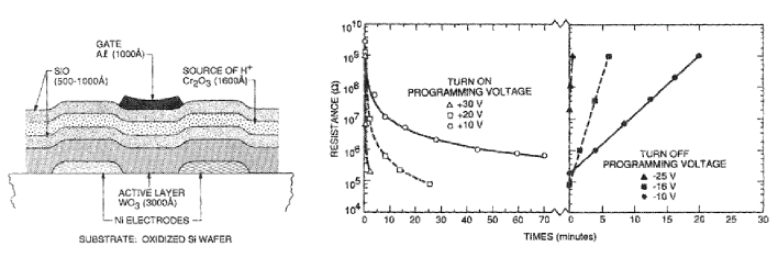
(b)
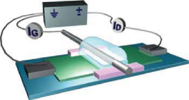 (c)
(c)
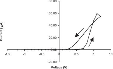
VI.1.2 Solid-state “memistor”
A solid-state realization of the memistor was reported by Thakoor et al. Thakoor et al. (1990) in 1990. In the solid-state memistor device schematically shown in figure 51(a), the programming voltage is applied to the gate electrode with respect to the two read electrodes positioned at the bottom of the structure. The read electrodes are separated by a layer of tungsten trioxide, WO3. The resistance of tungsten trioxide was varied due to a transfer of hydrogen ions H+ from a thin film of hydroscopic chromium oxide Cr2O3 into the WO3 active layer. It was suggested that a redox reaction (with describing the amount of H+ ions transferred into WO3)
converting the WO3 film into a conducting bronze during “turn-on” and the reverse reaction during “turn-off” is responsible for the variation of resistance Thakoor et al. (1990). The possibility of continuous analog programming of resistance in a wide range of values from to was demonstrated. Experimentally measured curves under programming conditions (see figure 51(a)) show a power-law relationship for the “turn-on” process, and an exponential relationship for “turn-off” process Thakoor et al. (1990). Such a different form of “turn-on” and “turn-off” curves was related to a generated emf that is in the same direction with the applied voltage in the “turn-off” process, and in the opposite direction during the “turn-on” one, thus facilitating and opposing ion transfer, respectively Thakoor et al. (1990).
VI.1.3 Polymeric transistor
In several recent papers Erokhin et al. (2005); Smerieri et al. (2008); Berzina et al. (2009, 2010) a polymeric transistor with memory was investigated. Although the demonstrated transistor is a three-terminal device, it was called a memristor in some of these publications. Here, in order to avoid confusion, we prefer to use the name “transistor with memory” because of the three terminals configuration.
The operation of polymeric transistors with memory is based on the possibility to reversibly change the conductivity of the conductive polymer emeraldin base polyaniline (PANI) between oxidized and reduced states using ion drift in a solid electrolyte (LiCl was used in initial studies Erokhin et al. (2005)). The observed variation of conductivity was about two orders of magnitude Erokhin et al. (2005) under bi-polar operational conditions. In figure 51(c) we show an example of curve for a polymeric transistor with memory.
It is interesting that in such devices the shape is sensitive to electrolyte composition Berzina et al. (2010). On this ground, an optimal electrolyte composition was determined Berzina et al. (2010). Moreover, possible applications of polymeric transistor with memory in adaptive networks mimicking to some extent the learning behavior of biological systems were suggested Erokhin et al. (2007) (see also section VII.2.1 where we discuss applications of three-terminal devices in neuromorphic circuits).
VI.2 Memristive component in Josephson junctions
In a realistic model of a Josephson junction Chua (2003), the latter is approximated by an equivalent scheme shown in figure 52 involving a linear resistor , linear capacitor , non-linear inductor and memristor connected in parallel (this model is also discussed in reference Jeltsema and van der Schaf (2010)). In this scheme, the memristor takes into account a small current component due to interference among quasi-particle pairs Chua (2003). The current through the memristor (we do not consider here the rest of the circuit since its modeling is standard, see, e.g., Likharev (1979)) is given by Overhauser (2000); Josephson (1962)
| (99) |
where and are device-related constants Chua (2003), and is the superconducting phase difference across the junction.
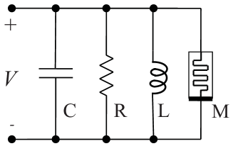
Since in the ac Josephson effect the phase difference evolves according to ( is the electron charge)
| (100) |
the equation (99) results in
| (101) |
which describes an ideal voltage-controlled memristor. We thus see that Josephson junctions contain a memristive component. This component is however generally small, and in most cases of practical interest it can be neglected. Nevertheless, this example is important since the memristive component in Josephson junctions is a rare example of ideal memristor.
| Physical system | Josephson junction |
|---|---|
| Internal state variable(s) | Phase difference, |
| Mathematical description | |
| System type | Voltage-controlled memristor |
VII Application of memory elements
There are several already well established applications of memory elements such as the use of thermistors or tunable capacitors employing MEMS. Here, we would like to focus instead on future potential applications. Such future applications of memory circuit elements are envisioned in both digital and analog domains. These mostly concern memristive systems, while those involving memcapacitive and meminductive systems are still at an early stage, even though certain applications discussed below (e.g., biologically-inspired circuits or logic) could be equally realized with these classes of systems.
In the digital domain, applications of memristive systems involve non-volatile solid-state memory, signal processing and programmable logic. Analog applications of memristive systems are based on the possibility to continuously vary their physical response and, therefore, on their ability to store more (theoretically infinite) information than in the digital regime. In this respect, these are related to analog signal processing, learning circuits, programmable analog circuits and neuromorphic circuits. Below we discuss such cases.
VII.1 Digital applications
VII.1.1 Digital memory
The digital binary non-volatile memory is the most straightforward and developed application of memristive systems. The current research efforts are primarily focused on this technological direction Karg et al. (2008); Csaba and Lugli (2009); Cagli et al. (2009); Vontobel et al. (2009); Strukov and Williams (2009b); Lian et al. (2010); Zhuge et al. (2010); Wu et al. (2005); Green et al. (2007). It is expected that the resistive random access memory (ReRAM) may replace Flash memory Lai (2008) in some years. Physically, a bit of information can be easily encoded in the memristive system’s state assigning, for example, the low resistance state to 1 and the high resistance state to 0. Moreover, the possibility of continuous variation of device’s resistance offers an opportunity for a multistate memory cell Nagashima et al. (2010); Moreno et al. (2010).
In table 16 we compare some basic technical characteristics of NAND (not AND gate-type) Flash memory and nanoionic ReRAM ITRS. The International Technology Roadmap for Semiconductors - ITRS 2009 Edition. http://www.itrs.net . Most of the demonstrated nanoionic ReRAM parameters are extracted from Ref. Dietrich et al. (2007) that reports fabrication of 2-Mbit CBRAM (Conductive Bridging Random Access Memory) utilizing 90nm technology. In this architecture, each memory cell contains one transistor and one memristive junction based on formation/disruption of a conductive bridge formed by Ag atoms in a germanium selenide chalcogenide material. The main advantage of ReRAM over Flash memory is in the significantly shorter read/write times. In addition, ReRAM technology is suitable for higher integration density circuit architecture by using a stack of crossbar arrays. The drawbacks of ReRAM include a low read voltage and relatively high write energy.
A single crossbar array ReRAM architecture is called CMOL Heath et al. (1998); Likharev and Strukov (2005) (Cmos+MOLecular-scale devices) combining a single crossbar layer (see figure 53(a)) with a conventional CMOS (complementary metal oxide semiconductor) layer. In the recently suggested three-dimensional extension of CMOL technology Strukov and Williams (2009b), a single CMOS layer is located underneath multiple crossbar layers separated by translation layers (figure 53(b)). In such an architecture, each memristive element can be accessed via a unique four-dimensional address (for a single crossbar layer, the address is two-dimensional) Strukov and Williams (2009b).
| Property | NAND Flash | Nanoionic ReRAM | ||
|---|---|---|---|---|
| Year/status | 2009 | 2024 | Demonstrated | Best projected |
| Feature size F (nm) | 90 | 18 | 90 | 5-10 |
| Cell area | 5F2 | 5F2 | 8F2 | 8/5F2 |
| Read time | 50 ns | 8ns | 50ns | 10ns |
| Write/Erase time | 1/0.1ms | 1/0.1ms | 5ns5ns | 20ns |
| Retention time | 10y | 10y | 10y | 10y |
| Write cycles | 1E5 | 1E5 | 1E9 | 1E16 |
| Write operating voltage (V) | 15 | 15 | 0.6/-0.2 | 0.5 |
| Read operating voltage (V) | 2 | 1 | 0.15 | 0.2 |
| Write emergy (Jbit) | 1E-14 | 1E-15 | 5E-14 | 1E-15 |
(a)
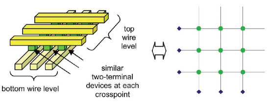
(b)
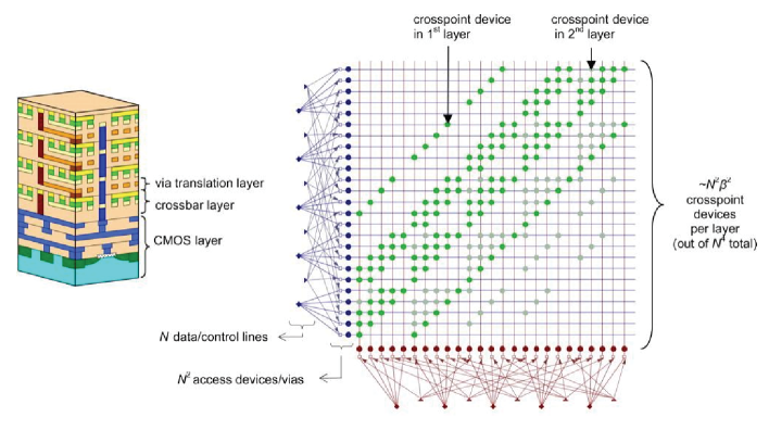
As we have noted in section III.2, the implementation of crossbar array memory may be complicated as a crossbar array represents a resistive network so that the current between any two selected word and bit lines can flow through many memristive devices. One of the approaches to overcome this problem is to use individual access devices such as diodes or transistors. Another approach was recently suggested by Wang and co-authors Wang et al. (2010a). In order to write information into a specific cell, they propose to apply and voltages to the corresponding word and bit lines and zero voltage to all other lines. In this way, only the selected cell will be subjected to voltage amplitude and all others cell will experience or bias. Assuming that the switching occurs when the applied voltage amplitude is above , the change of only selected cell becomes possible. A negative side of this approach is that the current still will flow through all memristive elements connected to two selected lines dramatically increasing the power dissipation when utilizing many-elements crossbar arrays.
A detailed overview of emergent storage memory technologies can be found in the review paper Burr et al. (2008).
VII.1.2 Logic
Another important application of memristive systems is in the field of digital logic circuits. On the one hand, memristive systems can serve as configuration bits and switches in a data routing network, and on the other hand they can be used to perform logic operations. In particular, Strukov and Likharev Strukov and Likharev (2005, 2007) have shown the potential of using CMOL circuits in the areas of field-programmable gate arrays (FPGAs) Strukov and Likharev (2005) and image processing Strukov and Likharev (2007). The efficiency analysis shows that memristive FPGAs are much faster and more energy efficient in comparison with similar traditional devices based on CMOS technology Cabe and Das (2009). Hybrid reconfigurable logic circuits Xia et al. (2009), and logic circuits with a “self-programming” capability Borghetti et al. (2009) (namely, with a capability of a circuit to reconfigure itself) were demonstrated. In both works, titanium-dioxide thin-film memristive systems were used as basic device structures.
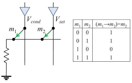
In stateful logic architecture, the “state” of the memristive system acts as both a logic gate and a latch (bi-stable circuit element capable to hold one bit of information). The concept of crossbar latch was discussed in reference Kuekes et al. (2005) where a device storing a logic value, enabling logic value restoration and inversion was demonstrated. It was concluded that such functionality, in combination with resistor/diode logic gates, enables universal computing Kuekes et al. (2005), namely given a description of any other computer or program and some data, it can perfectly emulate this second computer or program. Recently, Borghetti et al. have experimentally demonstrated a realization of material implication and NAND operation with memristive elements Borghetti et al. (2010). In addition, Lehtonen and Laiho Lehtonen and Laiho (2009); Lehtonen et al. (2010) have analyzed how many additional memristive elements, in addition to memristive systems holding initial values, are needed to compute any Boolean function. Their conclusion is that two memristive systems indeed suffice to compute all Boolean functions Lehtonen et al. (2010).
To understand logic operations with memristive systems, let us consider a realization of material implication shown in figure 54. In this circuit, voltages are used in circuit operation, state 0 corresponds to the high-resistance state of memristive systems, and state 1 is the low-resistance state, and the memristive systems are connected to a load resistor. The circuit operation is based on the threshold-type behavior of experimentally realizable memristive systems (see, e.g., the equation for in table 6). The calculation result is stored in .
First of all, we note that the amplitudes of and are selected in such a way that the voltage on never exceeds the threshold. Therefore, the state of remains unchanged. When is in the high resistance state (=0) and and are applied, the voltage on exceeds the threshold leading to the transition of from 0 to 1. However, under the same conditions but with =1, the voltage drop on is reduced and the transition of from 0 to 1 is prohibited. Symbolically, material implication operation can be expressed as
| (102) |
namely the logic operation is stored in . Material implication - together with the possibility of reset (by changing polarity of ) - are functionally complete, thus providing an opportunity to compute any Boolean function Lehtonen and Laiho (2009).
However, to the best of our knowledge, the actual sequences of operations to realize other logic gates were not reported anywhere in the literature. Therefore, below we provide the realization of the basic logic functions NOT, OR, and AND. In these operations, an additional work memristive element is used, which is also used to store the results.
| (103) | ||||
| (104) | ||||
| (105) | ||||
Based on material implication, an algorithm for adding two numbers was suggested Lehtonen and Laiho (2009). However, this operation requires a large number of steps. In order to overcome this deficiency, the present authors have suggested a modification of the circuit shown in Fig. 54 by adding a memcapacitive element Pershin and Di Ventra (2010c). In such a configuration, ”input” memristive systems can be distinguished from ”output” ones. The operation of the modified circuit is based on charging the memcapacitive system through the input memristive system and discharging it through output ones. This protocol requires smaller number of steps to perform both main logic and arithmetic operations. In fact, the basic logic operations (NOT, AND, OR) as well as addition of two one-bit numbers were experimentally demonstrated using memristor emulators Pershin and Di Ventra (2010c) (see also section VII.2.5).
We would like to point out that several hybrid circuit layouts were patented that could perform these types of operations (see, e.g., references Snider (2004); Mouttet (2006)). We also note that, since memory circuit elements are intrinsically analog devices (they acquire a continuous set of values within a certain range), they could also be used to generate “fuzzy logic” Klir and Yuan (1995), namely non-Boolean logic operations, such as statements of the type (IF variable IS property THEN action), , etc. However, we are not aware of any experimental (or theoretical) work in this direction.
VII.2 Analog applications
VII.2.1 Neuromorphic circuits
Another potential exciting application of memristive systems - and, possibly, the most important among analog applications - is in neuromorphic circuits. Neuromorphic circuits are circuits whose operation is meant to mimic that of the (human or animal) brain. In these circuits, memristive systems (and possibly also memcapacitive systems) can be used as synapses whose role is to provide connections between neurons and store information. As anticipated in section III.2.1, the small size of solid-state memristive systems is highly beneficial for this application since the density of memristive systems in a chip can be of the same order of magnitude as the density of synapses in human brains ( synapses/cm2) Snider (2008). Therefore, using memristive systems, the fabrication of an artificial neural network of a size comparable to that of a biological brain becomes possible.
An important feature of biological synapses is the spike-timing-dependent plasticity Levy and Steward (1983); Markram et al. (1997); Bi and Poo (1998); Froemke and Dan (2002). In fact, when a post-synaptic signal reaches the synapse before the action potential of the pre-synaptic neuron, the synapse shows long-term depression (LTD), namely its strength decreases (smaller connection between the neurons) depending on the time difference between the post-synaptic and the pre-synaptic signals. Conversely, when the post-synaptic action potential reaches the synapse after the pre-synaptic action potential, the synapse undergoes a long-time potentiation (LTP), namely the signal transmission between the two neurons increases in proportion to the time difference between the pre-synaptic and the post-synaptic signals. These general features of biological synapses can be implemented using different types of memristive systems Pershin and Di Ventra (2010c). We can distinguish three general approaches to STDP realization in artificial neural networks: using an overlap of asymmetric pulses Snider (2008); Parkin (2010); Pershin and Di Ventra (2010c), employing additional CMOS circuitry to track pulse timing Jo et al. (2010), and utilizing higher-order memristive systems with intrinsic pulse-timing tracking capability Pershin and Di Ventra (2010c).
A model of such a higher-order memristive system that is capable to track time separation between post- and pre-synaptic action potentials was suggested by the present authors in reference Pershin and Di Ventra (2010c). We provide the model’s details in table 17. In there, is a constant, is a threshold voltage, is a threshold value of the internal variable , is a constant defining the time window of STDP. It is assumed that short (e.g., ms width) pre-synaptic and post-synaptic square pulses of the same polarity are applied to the second-order memristive system. According to the equation for , the memristance can change when . The change of is described by an equation whose right-hand side contains excitation terms involving -functions and a relaxation term . Therefore, after being excited, the decay of the variable occurs with a decay constant . The particular combination of -functions in this equation defines the excitation rules: i) the excitation is possible only when and ii) the variable excited by a certain polarity of the voltage applied to the memristive system ( is given by a difference of pre-synaptic and post-synaptic potentials) can not be re-excited by a pulse of opposite polarity if . We also note that the change in memristance described by the equations in table 17 is constrained between and . These constraints are similar to those previously reported in table 6.
| Physical system | Artificial memristive synapse |
|---|---|
| Internal state variable(s) | Resistance and timing variable, , |
| Mathematical description | |
| System type | Second-order voltage-controlled memristive system |
Experimentally, several circuits showing neuromorphic behavior of different types and complexities were demonstrated Pershin and Di Ventra (2010a); Jo et al. (2010); Choi et al. (2009); Alibart et al. (2010); Lai et al. (2010). These circuits were based on two-terminal Pershin and Di Ventra (2010a); Jo et al. (2010); Choi et al. (2009) and three-terminal Alibart et al. (2010); Lai et al. (2010); Zhao et al. (2010) memristive devices. Jo et al. Jo et al. (2010) have demonstrated a spike-timing-dependent plasticity (STDP) using a crossbar array of Ag-based memristive synapses. In their architecture, CMOS elements were used to analyze timing of pre- and post-synaptic pulses in order to generate positive or negative memristive device programming pulses. In figure 55 we show a comparison of STDP of artificial synapses with changes in excitatory post-synaptic current of rat hippocampal neurons Jo et al. (2010). Choi and co-authors Choi et al. (2009) have built a crossbar array of GdOx/Cu-doped MoOx memory and demonstrated a weight sum operation important for neural networks.
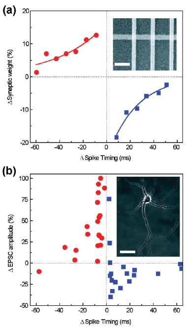
Three-terminal memristive devices employed in recent experiments Alibart et al. (2010); Lai et al. (2010) were of a transistor structure in which the gate electrode was typically used to induce resistance changes probed by a current through two other electrodes. Lai and co-workers Lai et al. (2010) have demonstrated a synaptic transistor showing STDP. They have used a conventional MOS transistor structure with a conjugated polymer (MEH-PPV) layer and a layer of ionic conductor RbAg4I5 placed below the gate electrode. Peculiar features of their experiments are paired spikes composed of 1ms positive and 1ms negative voltage pulses. In figure 56 an experimentally measured STDP of such synaptic devices is demonstrated. Alibart et al. Alibart et al. (2010) have fabricated a nanoparticle organic memory field-effect transistor (NOMFET) whose memory response is due to charging gold nanoparticles embedded into a layer of pentacene thin film. Using this NOMFET they have observed facilitating and depressing synaptic behavior. Possible drawbacks of this approach include charge leaking limiting retention time in the range of a few seconds to a few thousand of seconds and high amplitude voltage (V) needed for circuit operation Alibart et al. (2010). In a recent paper Zhao et al. (2010), a crossbar array architecture integrating optically-gated carbon nanotubes was also suggested for neuromorphic applications.
(a)
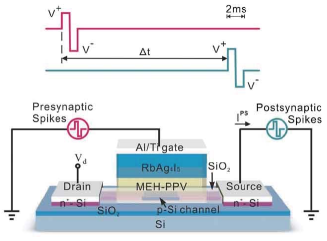 (b)
(b)
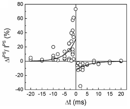
Pershin and Di Ventra Pershin and Di Ventra (2010a) have reported the experimental realization of a neural network based on memristor emulators (see section VII.2.5 for their electronic scheme) demonstrating associative learning. The neural network used in that experimental study contains two memristive synapses and three neurons as shown in figure 57. Associative memory is a fundamental property of the animal brain closely related to the so-called Pavlovian training Pavlov (1927) in which a particular response to a given stimulus develops. The most notable experiment of associative memory is that of a dog to which food is shown and, at the same time, the tone of a bell is rang so that, with time, the dog salivates at the ring of the bell only. In the electronic three-neuron network described in reference Pershin and Di Ventra (2010a), two input neurons were responsible for the “sight of food” and “sound” events, while the output neuron generated a “salivation” command.
Figure 58 demonstrates experimental results of the neural network operation. The functioning of the electronic circuits is essentially based on pulse overlapping. When Input 1 is excited, the first neuron sends forward positive-polarity pulses that excite the third neuron which starts sending positive pulses in the forward direction and negative pulses backward. If, at the same time, the second neuron is also excited, the overlap of positive pulses from this second neuron and negative pulses from the third neuron over memristive synapse results in a voltage on exceeding its threshold. In this way, the resistance decreases, or, in other words, an association develops.
If we return to figure 58 again, it clearly shows that, if one starts with an untrained state of the synapse connecting the input “sound” neuron and output neuron and exposes the neural network to “sight of food” and “sound” signals simultaneously, then an association between “food” and “sound” develops and an output signal is generated when only the “sound” input signal is applied. This is exactly the associative memory behavior discussed above.
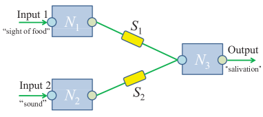
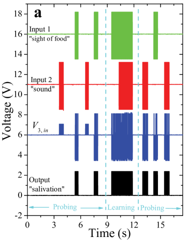
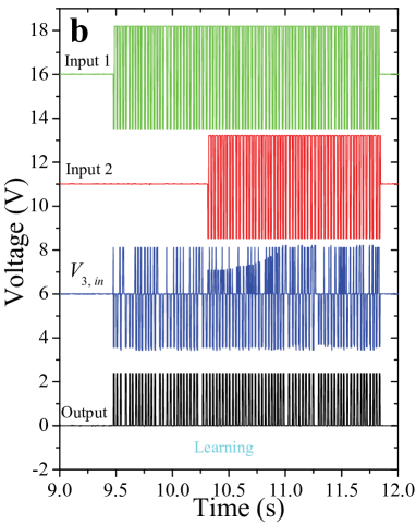
VII.2.2 Quantum computing with memory circuit elements
Memcapacitive and meminductive systems may find useful applications in electronic circuits with superconducting qubits Clarke and Wilhelm (2008); Zagoskin and Blais (2007). Since typical superconducting qubit circuits involve usual capacitors and inductors Clarke and Wilhelm (2008); Zagoskin and Blais (2007), certain memcapacitive and meminductive elements are ideal for such circuits. What are the advantages of using memory elements in superconducting qubit circuits? One of many possible applications is field-programmable quantum computing that was recently discussed by the present authors Pershin and Di Ventra (2010c). The idea is to replace capacitive (inductive) elements that provide coupling between different qubits by non-dissipative memcapacitive (meminductive) elements, and introduce additional voltage sources to control the state of these memory elements. In this way, the coupling strength between qubits can be selected. If we consider simultaneously interacting qubits then a variation of coupling between two of them will result in absolutely different interaction Hamiltonians thus leading to a different system evolution. Quantum computation algorithms will thus benefit from such novel quantum hardware functionality because of the many (practically infinite) interaction schemes that can be implemented within a single circuit architecture Pershin and Di Ventra (2010c). We would like to note, however, that for such application we envision memcapacitive and meminductive elements that are non-dissipative (at least within certain time scales), so that they do not introduce additional qubit relaxation/decoherence.
It might be well to point out that Josephson junctions coupled with nanomechanical resonators were studied in the past Cleland and Geller (2004); Buks and Blencowe (2006); Zhou and Mizel (2006); Zhang et al. (2009); Pugnetti et al. (2010). For example, it was shown in reference Cleland and Geller (2004) that a nanomechanical resonator consisting of a piezoelectric crystal sandwiched between split metal electrodes can be used to provide coupling between phase qubits. Such a resonator has signatures of a memcapacitive system in which elastic vibrations plays an important role. However, the coupling provided by the resonator is of a constant strength Cleland and Geller (2004) and, therefore, it can not be directly used for the field-programmable quantum computing idea discussed above.
VII.2.3 Learning circuits
Quite generally, a “learning circuit” is an electronic circuit whose response at a given time adapts according to signals applied to the circuit at previous moments of time Pershin et al. (2009). All three memory circuit elements are ideal components for such a circuit since they provide non-volatile information storage and compatibility (as time-dependent devices) with other circuit elements. The present authors have recently suggested Pershin et al. (2009) a learning circuit which mimics adaptive behavior of a slime mold Physarum polycephalum from the group of amoebozoa. This work was inspired by recent experimental observations on this unicellular organism Saigusa et al. (2008). These experiments have shown that when Physarum polycephalum is exposed to a pattern of periodic environment changes (of temperature and humidity), it “learns” and adapts its behavior in anticipation of the next stimulus to come. We have shown Pershin et al. (2009) that such behavior can be described by the response of a simple electronic circuit as that shown in figure 59(a). The circuit is composed of an LC contour and a memristive system in parallel with the capacitor. The memristive system was described by the equations presented in table 6 that was introduced in section III.2.4. This model takes into account the non-linear memristance rate of change defined by two parameters and (see also figure 59(a)).
Figure 59(b) represents simulation results of the response of the circuit. When a periodic signal is applied to the learning circuit, the voltage across the capacitor significantly changes and can exceed the threshold voltage of the memristive system. This leads to an increase in the resistance of the memristive system and, consequently, in a smaller damping of the LC contour. Therefore, the LC contour oscillations are maintained for a longer period of time in analogy with the same type of behavior observed when the amoeba is subject to periodic environment changes.
(a)
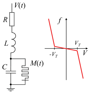 (b)
(b)
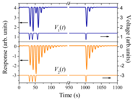
Very recently, an electronic circuit Driscoll et al. (2010b) having a close similarity to the learning circuit in Fig. 59(a) was experimentally implemented. In this circuit, a vanadium dioxide memristive system was placed into an contour. It was demonstrated that the application of specific frequency signals sharpens the quality factor of its resonant response, and thus the circuit learns according to the input waveform.
VII.2.4 Programmable analog circuits
In programmable analog circuits, memristive systems that operate under threshold conditions (as those described in the previous section) can be used as digital potentiometers Pershin and Di Ventra (2010d). The main idea is to apply small amplitude voltages to memristive systems when they are used as analog circuit elements, and high amplitude voltage pulses for the purpose of resistance programming. Since the state of memristive system appreciably changes only when the voltage applied to it exceeds a certain threshold Strukov and Williams (2009a), its resistance is constant in the analog mode of operation, and changes by discrete values with each voltage pulse. Using this idea, several programmable analog circuits demonstrating memristive system-based programming of threshold, gain and frequency were demonstrated by these authors Pershin and Di Ventra (2010d).
VII.2.5 Emulators of memristive, memcapacitive and meminductive systems
All of the above mentioned programmable analog circuits were built using a memristor emulator Pershin and Di Ventra (2010d) which is schematically shown in figure 60(a). It consists of a microcontroller-controlled digital potentiometer whose resistance value is calculated by the microcontroller using equations of a current-controlled or voltage-controlled memristive system. For these calculations, the value of the voltage applied to the scheme is provided by an analog-to-digital converter. Since virtually almost any set of memristive system equations can be pre-programmed, the memristor emulator offers a unique opportunity to simulate memristive behavior in electronic circuits.
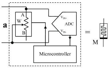
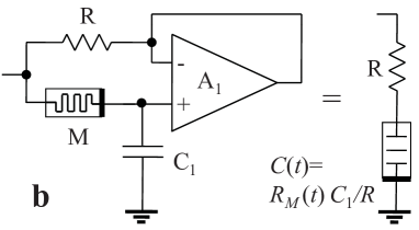
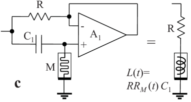
Moreover, the present authors have suggested that specific circuits with memristive systems can emulate an effective memcapacitive and meminductive behavior Pershin and Di Ventra (2010b). The architecture of such circuits (see figure 60 (b,c)) is based on the gyrator scheme. In both memcapacitive system and memindictive system emulators, memory properties of the memristor emulator described above are effectively transferred into an effective memcapacitive and meminductive response.
For instance, let us consider the circuit of memcapacitive system emulator depicted in figure 60 (b). In this scheme, since the operational amplifier keeps nearly equal voltages at its positive and negative inputs, the voltage on the capacitor is applied to the right terminal of . Therefore, we can think that an effective capacitor with a time-dependent capacitance is connected to the right terminal of , so that the relation holds.
Let us assume that a voltage-controlled memristive system is used in the memcapacitive system emulator. Then, equations describing the effective memcapacitor are given by
| (106) | |||||
| (107) | |||||
| (108) |
where is the applied voltage and is the voltage on the capacitor . In equations (106-108), acts as an additional state variable of the effective memcapacitive system. In fact, this is not surprising since the capacitor (in figure 60(b)) stores information in the form of charge. Consequently, the order of the effective voltage-controlled memcapacitive system exceeds the order of the memristive system by one.
The operation of the meminductive system emulator in figure 60(c) can be understood in a similar manner. These emulators also show an interesting connection between the three memory elements. However, we need to stress that since the memcapacitive system and meminductive system emulators involve an extra internal resistance, they do not behave as single (perfect) memcapacitive or meminductive systems. Recently, Biolek and Biolkova Biolek and Biolkova (2010) have suggested a different scheme (mutator) transforming memristive behavior into memcapacitive one. Their approach utilizes two operational transimpedance amplifiers operating as the current conveyors. The suggested scheme responds as an ideal memcapacitive system without an additional resistance as that shown in the equivalent scheme in figure 60(b).
VII.2.6 Other circuits
There are a few other memristive system-based analog circuits discussed in the literature Shima et al. (2009); Wey and Benderli (2009); Bray and Werner (2010). In particular, an interesting method of using memristive systems as passive electromagnetic switches was suggested and analyzed by Bray and Werner Bray and Werner (2010). Way and Benderli Wey and Benderli (2009) have simulated and analyzed an architecture of an amplitude-modulation circuit. A circuit element combining diode and memory resistance properties, the switchable rectifier, was proposed and built by Shima et al. Shima et al. (2009). Their device based on Pt/TiOx/Pt structure demonstrates a reproducible switching. Such a circuit element can find useful applications in both analog and digital domains.
Moreover, several authors have investigated chaotic circuits with memristors Itoh and Chua (2008); Muthuswamy and Kokate (2009); Qi-Shui et al. (2010); Bao et al. (2010); Bo-Cheng et al. (2010); Messias et al. (2010). For the most part modified Chua’s oscillators Matsumoto (1984); Madan (1993) were considered Itoh and Chua (2008); Muthuswamy and Kokate (2009); Bao et al. (2010); Bo-Cheng et al. (2010). In such an approach, the active nonlinear resistance element, Chua’s diode Madan (1993), is replaced by an active memristor (as we show in figure 61) and novel features in chaotic behavior are observed Itoh and Chua (2008); Muthuswamy and Kokate (2009); Bao et al. (2010); Bo-Cheng et al. (2010). An active memristor is one for which Eq. (30) is not satisfied. In fact, one such circuit was implemented experimentally Muthuswamy (2010). We have, however, recently shown that chaotic behavior does not require active memristors and even a single memristive system driven by an ac voltage can manifest chaos Driscoll et al. (2010a). Moreover, chaos is observed when an ac-voltage is applied to the bistable membrane memcapacitive system considered in section IV.1.2 Martinez-Rincon and Pershin (2010). Apart from interesting fundamental studies of non-linear systems, the field of applications of such circuits includes secure communications with chaos Muthuswamy and Kokate (2009).
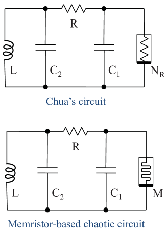
VIII Conclusions and outlook
In this review we have shown that memory effects are ubiquitous in complex materials and nanoscale systems. This memory manifests itself under several physical properties - related to charge, spin, and structural dynamics - which, however, can be generally categorized as memristive, memcapacitive and meminductive, or a combination of these. The advantage of these elements is based on a combination of a history-dependent behavior with properties of basic circuit elements - such as resistors, capacitors or inductors. The realization of this link between the underlying physical properties that lead to memory and their description in terms of memory circuit elements opens up unprecedented opportunities in both fundamental science and applications, since it guides the discovery of novel functionalities, inspires new concepts and connections between apparently diverse fields, and in certain cases it also allows a reconsideration of old concepts from a totally new perspective. Cagli et al. (2009)
We have provided a large set of examples of systems where these memory effects are observed or expected. Clearly, due to the necessary space limitations of this review we are far from having exhausted all possible physical systems and devices that show these features. Indeed, as we have also emphasized in this review, we firmly think that due to the continued miniaturization of devices, many more systems will be discovered that show memory. This confidence is supported by the physical fact that the change of state of electrons and ions is not instantaneous, rather it generally depends on the past dynamics.
We have also discussed many applications, ranging from information storage to learning/programmable circuits to biologically-inspired systems. In some cases, we also expect that the cost of certain practical implementations of these elements should be relatively low in view of their simple structure. It is thus not too unlikely that some of the systems we have discussed in this review may develop into commercially available products in the coming years, and find their own niche of applications. We therefore anticipate that novel exciting applications will be developed with beneficial impact not only for technology but also for fundamental science.
Acknowledgments
This work has been partially funded by the NSF grant No. DMR-0802830.
References
- Alexandrov and Bratkovsky (2009) Alexandrov, A. S., and A. M. Bratkovsky, 2009, Phys. Rev. B 80, 115321.
- Alibart et al. (2010) Alibart, F., S. Pleutin, D. Guerin, C. Novembre, S. Lenfant, K. Lmimouni, C. Gamrat, and D. Vuillaume, 2010, Adv. Funct. Mat. 20, 330.
- de Almeida et al. (2002) de Almeida, L. A. L., G. S. Deep, A. M. N. Lima, and H. Neff, 2002, Optical Engineering 41(10), 2582.
- Arcangeletti et al. (2007) Arcangeletti, E., L. Baldassarre, D. Di Castro, S. Lupi, L. Malavasi, C. Marini, A. Perucchi, and P. Postorino, 2007, Phys. Rev. Lett. 98(19), 196406.
- Argall (1968) Argall, F., 1968, Solid-State Electronics 11, 535.
- Asamitsu et al. (1997) Asamitsu, A., Y. Tomioka, H. Kuwahara, and Y. Tokura, 1997, Nature 388, 50.
- Attema et al. (2006) Attema, J. J., G. A. de Wijs, and R. A. de Groot, 2006, Journal of Physics D: Applied Physics 39(5), 793.
- Baikalov et al. (2003) Baikalov, A., Y. Wang, B. Shen, B. Lorenz, S. Tsui, Y. Sun, Y. Xue, and C. Chu, 2003, Appl. Phys. Lett. 83(5), 957.
- Bao et al. (2010) Bao, B. C., Z. Liu, and J. P. Xu, 2010, El. Lett. 46(3), 228.
- Benderli and Wey (2009) Benderli, S., and T. A. Wey, 2009, El. Lett. 45, 377.
- Berger (1978) Berger, L., 1978, J. Appl. Phys. 49, 2156.
- Berzina et al. (2009) Berzina, T., A. Smerieri, M. Bernabo, A. Pucci, G. Ruggeri, V. Erokhin, and M. P. Fontana, 2009, J. Appl. Phys. 105(12), 124515.
- Berzina et al. (2010) Berzina, T., A. Smerieri, G. Ruggeri, M. Bernabo’, V. Erokhin, and M. Fontana, 2010, Materials Science and Engineering: C 30(3), 407, ISSN 0928-4931.
- Bi and Poo (1998) Bi, G. Q., and M. M. Poo, 1998, J. Neurosci. 18, 10464.
- Biolek et al. (2010a) Biolek, D., Z. Biolek, and V. Biolkova, 2010a, Analog Integr. Circ. Sig. Process., available online .
- Biolek et al. (2010b) Biolek, D., Z. Biolek, and V. Biolkova, 2010b, El. Lett. 46, 520.
- Biolek and Biolkova (2010) Biolek, D., and V. Biolkova, 2010, El. Lett. 46, 1428.
- Biolek et al. (2009a) Biolek, Z., D. Biolek, and V. Biolkova, 2009a, Radioengineering 18, 210.
- Biolek et al. (2009b) Biolek, Z., D. Biolek, and V. Biolkova, 2009b, Proc. of ECCTD ’09, European Conference on Circuit Theory and Design , 249.
- Bo-Cheng et al. (2010) Bo-Cheng, B., L. Zhong, and X. Jian-Ping, 2010, Chin. Phys. B 19, 030510.
- Borghetti et al. (2009) Borghetti, J., Z. Li, J. Straznicky, X. Li, D. A. A. Ohlberg, W. Wu, D. R. Stewart, and R. S. Williams, 2009, Proc. Nat. Ac. Sci. 106, 1699.
- Borghetti et al. (2010) Borghetti, J., G. S. Snider, P. J. Kuekes, J. J. Yang, D. R. Stewart, and R. S. Williams, 2010, Nature 464, 873.
- Branton et al. (2008) Branton, D., D. W. Deamer, A. Marziali, H. Bayley, S. A. Benner, T. Butler, M. Di Ventra, S. Garaj, A. Hibbs, X. Huang, S. B. Jovanovich, P. S. Krstic, et al., 2008, Nat. Biotechnol. 26(10), 1146.
- Brataas et al. (2006) Brataas, A., G. Bauer, and P. Kelly, 2006, Phys. Rep. 427(4), 157.
- Bratkovsky (2008) Bratkovsky, A. M., 2008, Reports on Progress in Physics 71, 026502.
- Bray and Werner (2010) Bray, M. G., and D. H. Werner, 2010, Appl. Phys. Lett. 96, 073504.
- Buks and Blencowe (2006) Buks, E., and M. P. Blencowe, 2006, Phys. Rev. B 74, 174504.
- Burr et al. (2008) Burr, G. W., B. N. Kurdi, J. C. Scott, C. H. Lam, K. Gopalakrishnan, and R. S. Shenoy, 2008, IBM J. Res. Dev. 52, 449.
- Cabe and Das (2009) Cabe, A. C., and S. Das, 2009, Nanotechn. 20, 165203.
- Cagin et al. (2007) Cagin, E., D. Y. Chen, J. J. Siddiqui, and J. D. Phillips, 2007, Journal of Physics D: Applied Physics 40(8), 2430.
- Cagli et al. (2009) Cagli, C., F. Nardi, and D. Ielmini, 2009, IEEE Trans. El. Dev. 56(8), 1712.
- Cai et al. (2005) Cai, L., M. Cabassi, H. Yoon, O. Cabarcos, C. McGuiness, A. Flatt, D. Allara, J. Tour, and T. Mayer, 2005, Nano Lett. 5, 2365.
- Cavalleri et al. (2004) Cavalleri, A., T. Dekorsy, H. H. W. Chong, J. C. Kieffer, and R. W. Schoenlein, 2004, Phys. Rev. B 70(16), 161102.
- Chang and Sivoththaman (2006) Chang, S., and S. Sivoththaman, 2006, IEEE El. Dev. Lett. 27(11), 905.
- Chen et al. (1986) Chen, M., K. A. Rubin, and R. W. Barton, 1986, Appl. Phys. Lett. 49, 502.
- Choi et al. (2005) Choi, B., D. Jeong, S. Kim, C. Rohde, S. Choi, J. Oh, H. Kim, C. Hwang, K. Szot, R. Waser, B. Reichenberg, and S. Tiedke, 2005, J. Appl. Phys. 98, 033715.
- Choi et al. (2008a) Choi, H., B.-S. Choi, T.-W. Kim, S.-J. Jung, M. Chang, T. Lee, and H. Hwang, 2008a, Nanotechnology 19, 305704.
- Choi et al. (2009) Choi, H., H. Jung, J. Lee, J. Yoon, J. Park, D.-J. Seong, W. Lee, M. Hasan, G.-Y. Jung, and H. Hwang, 2009, Nanotechn. 20, 345201.
- Choi et al. (2008b) Choi, S., S.-H. Hong, S. H. Cho, S. Park, S.-M. Park, O. Kim, and M. Ree, 2008b, Adv. Mat. 20(9), 1766+.
- Chu et al. (1993) Chu, W.-H., M. Mehregany, and R. L. Mullen, 1993, J. Micromech. Microeng. 3, 4.
- Chua (1971) Chua, L. O., 1971, IEEE Trans. Circuit Theory 18, 507.
- Chua (2003) Chua, L. O., 2003, Proc. IEEE 91, 1830.
- Chua and Kang (1976) Chua, L. O., and S. M. Kang, 1976, Proc. IEEE 64, 209.
- Claassen et al. (2010) Claassen, J. H., J. W. Lu, K. G. West, and S. A. Wolf, 2010, Appl. Phys. Lett. 96, 132102.
- Clarke and Wilhelm (2008) Clarke, J., and F. K. Wilhelm, 2008, Nature 453, 1031.
- Cleland and Geller (2004) Cleland, A. N., and M. R. Geller, 2004, Phys. Rev. Lett. 93, 070501.
- Crowley (1973) Crowley, J. M., 1973, Biophysical journal 13, 711.
- Csaba and Lugli (2009) Csaba, G., and P. Lugli, 2009, IEEE Trans. Nanotechn. 8, 369.
- Dawber et al. (2005) Dawber, M., K. M. Rabe, and J. F. Scott, 2005, Rev. Mod. Phys. 77(4), 1083.
- Dearnaley et al. (1970) Dearnaley, G., A. M. Stoneham, and D. V. Morgan, 1970, Reports on Progress in Physics 33, 1129.
- Di Ventra (2008) Di Ventra, M., 2008, Electrical Transport in Nanoscale Systems (Cambridge University Press).
- Di Ventra et al. (2009) Di Ventra, M., Y. V. Pershin, and L. O. Chua, 2009, Proc. IEEE 97(10), 1717.
- Dietrich et al. (2007) Dietrich, S., M. Angerbauer, M. Ivanov, D. Gogl, H. Hoenigschmid, M. Kund, C. Liaw, M. Markert, R. Symanczyk, L. Altimime, S. Bournat, and G. Mueller, 2007, IEEE J. Sol.-State Circ. 42, 839.
- Dimitrakis et al. (2003) Dimitrakis, P., E. Kapetanakis, P. Normand, D. Skarlatos, D. Tsoukalas, K. Beltsios, A. Claverie, G. Benassayag, C. Bonafos, D. Chassaing, M. Carrada, and V. Soncini, 2003, Materials Science and Engineering B 101(1-3), 14, ISSN 0921-5107, eMRS 2002 Symposium S: Micro- and Nano-structured Semiconductors.
- Do et al. (2009) Do, Y. H., J. S. Kwak, J. P. Hong, H. Im, and B. H. Park, 2009, J. Kor. Phys. Soc. 55, 1009.
- Dong et al. (2008) Dong, Y., G. Yu, M. C. McAlpine, W. Lu, and C. M. Lieber, 2008, Nano Lett. 8(2), 386.
- Driscoll et al. (2009a) Driscoll, T., H.-T. Kim, B. G. Chae, M. Di Ventra, and D. N. Basov, 2009a, Appl. Phys. Lett. 95, 043503.
- Driscoll et al. (2009b) Driscoll, T., H.-T. Kim, B.-G. Chae, B.-J. Kim, Y.-W. Lee, N. M. Jokerst, S. Palit, D. R. Smith, M. Di Ventra, and D. N. Basov, 2009b, Science 325, 1518.
- Driscoll et al. (2008) Driscoll, T., S. Palit, M. M. Qazilbash, M. Brehm, F. Keilmann, B.-G. Chae, S.-J. Yun, H.-T. Kim, S. Y. Cho, N. M. Jokerst, D. R. Smith, and D. N. Basov, 2008, Appl. Phys. Lett. 93, 024101.
- Driscoll et al. (2010a) Driscoll, T., Y. V. Pershin, D. N. Basov, and M. Di Ventra, 2010a, submitted for publication .
- Driscoll et al. (2010b) Driscoll, T., J. Quinn1, S. Klein, H. T. Kim, B. J. Kim, Y. V. Pershin, M. Di Ventra, and D. N. Basov, 2010b, Appl. Phys. Lett. 97, 093502.
- Ducharne et al. (2007) Ducharne, B., D. Guyomar, and G. Sebald, 2007, Journal of Physics D: Applied Physics 40(2), 551.
- Duine et al. (2007) Duine, R. A., A. S. Núñez, and A. H. MacDonald, 2007, Phys. Rev. Lett. 98(5), 056605.
- Dyakonov and Perel (1971) Dyakonov, M. I., and V. I. Perel, 1971, Physics Letters A 35(6), 459.
- Erokhin et al. (2005) Erokhin, V., T. Berzina, and M. Fontana, 2005, J. Appl. Phys. 97, 064501.
- Erokhin et al. (2007) Erokhin, V. V., T. S. Berzina, and M. P. Fontana, 2007, Crystallogr. Rep. 52, 159.
- Evoy et al. (2004) Evoy, S., M. Duemling, and T. Jaruhar, 2004, in Introduction to Nanoscale Science and Technology, edited by M. Di Ventra, S. Evoy, and J. R. Heflin (Springer), pp. 389–416.
- Fors et al. (2005) Fors, R., S. I. Khartsev, and A. M. Grishin, 2005, Phys. Rev. B 71, 045305.
- Froemke and Dan (2002) Froemke, R. C., and Y. Dan, 2002, Nature 416, 433.
- Gergel-Hackett et al. (2009) Gergel-Hackett, N., B. Hamadani, B. Dunlap, J. Suehle, C. Richter, C. Hacker, and D. Gundlach, 2009, IEEE El. Dev. Lett. 30, 706.
- Gilbert (1955) Gilbert, T. L., 1955, Phys. Rev. 100, 1243.
- Green et al. (2007) Green, J. E., J. W. Choi, A. Boukai, Y. Bunimovich, E. Johnston-Halperin, E. DeIonno, Y. Luo, B. A. Sheriff, K. Xu, Y. S. Shin, H.-R. Tseng, J. F. Stoddart, et al., 2007, Nature 445, 414.
- Ha and Kim (2008) Ha, H., and O. Kim, 2008, Apl. Phys. Lett. 93(3).
- Ha and Kim (2009) Ha, H., and O. Kim, 2009, Jpn. J. Appl. Phys. 48, 04C169.
- H.B. et al. (2007) H.B., C., K. Shin, and J. M. Lee, 2007, J. Vac. Sci. Technol. A25, 48.
- Heath et al. (1998) Heath, J., P. Kuekes, G. Snider, and R. Williams, 1998, Science 280(5370), 1716.
- Herfst et al. (2008) Herfst, R. W., P. G. Steeneken, H. G. A. B. Huizing, and J. Schmitz, 2008, IEEE Transactions on semiconductor manufacturing 21, 148.
- Hickmott (1962) Hickmott, T. W., 1962, J. Appl. Phys. 33, 2669.
- Hodgkin and Huxley (1952) Hodgkin, A. L., and A. F. Huxley, 1952, Journal of Physiology 117, 500.
- Ielmini and Zhang (2007) Ielmini, D., and Y. Zhang, 2007, J. Appl. Phys. 102, 054517.
- Imada et al. (1998) Imada, M., A. Fujimori, and Y. Tokura, 1998, Rev. Mod. Phys. 70(4), 1039.
- Inoue et al. (2008) Inoue, I. H., S. Yasuda, H. Akinaga, and H. Takagi, 2008, Phys. Rev. B 77, 035105.
- Itoh and Chua (2008) Itoh, M., and L. O. Chua, 2008, Int. J. Bif. Chaos 18, 3183.
- (84) ITRS. The International Technology Roadmap for Semiconductors - ITRS 2009 Edition. http://www.itrs.net, 2009.
- Iwasaki et al. (1993) Iwasaki, H., M. Harigaya, O. Nonoyama, Y. Kageyama, M. Takahashi, K. Yamada, H. Deguchi, and Y. Ide, 1993, Jpn. J. Appl. Phys. 32, 5241.
- Jang et al. (2008) Jang, J. E., S. N. Cha, Y. J. Choi, D. J. Kang, T. P. Butler, D. G. Hasko, J. E. Jung, J. M. Kim, and G. A. J. Amaratunga, 2008, Nature Nanotechnology 3, 26.
- Jeltsema and van der Schaf (2010) Jeltsema, D., and A. J. van der Schaf, 2010, Mathematical and Computer Modelling of Dynamical Systems 16, 75.
- Jeong et al. (2007) Jeong, D. S., H. Schroeder, and R. Waser, 2007, Electrochem. Sol. St. Lett. 10(8), G51.
- Jeong et al. (2009a) Jeong, D. S., H. Schroeder, and R. Waser, 2009a, Nanotechn. 20, 375201.
- Jeong et al. (2009b) Jeong, D. S., H. Schroeder, and R. Waser, 2009b, Phys. Rev. B 79, 195317.
- Jeong et al. (2009c) Jeong, H. Y., J. Y. Lee, S.-Y. Choi, and J. W. Kim, 2009c, Appl. Phys. Lett. 95, 162108.
- Jo et al. (2010) Jo, S. H., T. Chang, I. Ebong, B. B. Bhadviya, P. Mazumder, and W. Lu, 2010, Nano Lett. 10, 1297.
- Jo et al. (2009) Jo, S. H., K.-H. Kim, and W. Lu, 2009, Nano Lett. 9, 870.
- Jo and Lu (2008) Jo, S. H., and W. Lu, 2008, Nano Lett. 8(2), 392.
- Joglekar and Wolf (2009) Joglekar, Y. N., and S. J. Wolf, 2009, Eur. J. Phys. 30, 661.
- Josephson (1962) Josephson, B., 1962, Phys. Lett. 1(7), 251.
- Kandel et al. (2000) Kandel, E. R., J. H. Schwartz, and T. M. Jessell, 2000, Principles of Neural Science (McGraw-Hill Medical), 4th edition.
- Kang et al. (2003) Kang, D. H., D. H. Ahn, K. B. Kim, J. F. Webb, and K. W. Yi, 2003, J. Appl. Phys. 94, 3536.
- Kanoun et al. (2006) Kanoun, M., C. Busseret, A. Poncet, A. Souifi, T. Baron, and E. Gautier, 2006, Solid-State Electronics 50, 1310.
- Karg et al. (2008) Karg, S. F., G. I. Meijer, J. G. Bednorz, C. T. Rettner, A. G. Schrott, E. A. Joseph, C. H. Lam, M. Janousch, U. Staub, F. La Mattina, S. F. Alvarado, D. Widmer, et al., 2008, IBM J. Res. Dev. 52(4-5), 481.
- Kholkin et al. (2002) Kholkin, A. L., R. Martins, H. guas, I. Ferreira, V. Silva, O. A. Smirnova, M. E. V. Costa, P. M. Vilarinho, E. Fortunato, and J. L. Baptista, 2002, Journal of Non-Crystalline Solids 299-302(Part 2), 1311, ISSN 0022-3093.
- Kim et al. (2007a) Kim, B.-J., Y. W. Lee, B.-G. Chae, S. J. Yun, S.-Y. Oh, H.-T. Kim, and Y.-S. Lim, 2007a, Appl. Phys. Lett. 90, 023515.
- Kim et al. (2006a) Kim, D., S. Seo, S. Ahn, D. Suh, M. Lee, B. Park, I. Yoo, I. Baek, H. Kim, E. Yim, J. Lee, S. Park, et al., 2006a, Appl. Phys. Lett. 88, 202102.
- Kim et al. (2007b) Kim, D.-H., F. Merget, M. Forst, and H. Kurz, 2007b, J. Appl. Phys. 101, 064512.
- Kim et al. (2006b) Kim, D. S., Y. H. Kim, C. E. Lee, and Y. T. Kim, 2006b, Phys. Rev. B 74, 174430.
- Kim et al. (2006c) Kim, H.-T., Y. W. Lee, B.-J. Kim, B.-G. Chae, S. J. Yun, K.-Y. Kang, K.-J. Han, K.-J. Yee, and Y.-S. Lim, 2006c, Phys. Rev. Lett. 97(26), 266401.
- Kim et al. (2010) Kim, J., C. Ko, A. Frenzel, S. Ramanathan, and J. E. Hoffman, 2010, Appl. Phys. Lett. 96, 213106.
- Kim et al. (2007c) Kim, J. H., D. W. Kim, H. S. Jeon, and B. E. Park, 2007c, Jpn. J. Appl. Phys. 46, 6976.
- Kim et al. (2002) Kim, Y., H. J. Cheong, K. H. Park, T. H. Chung, H. J. Bark, J.-Y. Yi, S. H. Bang, and J. H. Cho, 2002, Semiconductor Science and Technology 17(10), 1039.
- Kim et al. (2001) Kim, Y., K. H. Park, T. H. Chung, H. J. Bark, J. Y. Yi, W. C. Choi, E. K. Kim, J. W. Lee, and J. Y. Lee, 2001, Appl. Phys. Lett. 78, 934.
- King et al. (2001) King, Y., T. King, and C. Hu, 2001, IEEE Trans. El. Dev. 48, 696.
- Klir and Yuan (1995) Klir, G. J., and B. Yuan, 1995, Fuzzy Sets and Fuzzy Logic: Theory and Applications (Prentice Hall), 1st edition.
- Kobayashi et al. (1997) Kobayashi, T., T. Endoh, H. Fukuda, S. Nomura, A. Sakai, and Y. Ueda, 1997, Appl. Phys. Lett. 71, 1195.
- Kozicki et al. (2005) Kozicki, M., M. Park, and M. Mitkova, 2005, IEEE Trans. Nanotechn. 4, 331.
- Krems et al. (2010) Krems, M., Y. V. Pershin, and M. Di Ventra, 2010, Nano Lett. 10, 2674.
- Krzysteczko et al. (2009) Krzysteczko, P., G. Reiss, and A. Thomas, 2009, Appl. Phys. Lett. 95, 112508.
- Kübler et al. (2007) Kübler, C., H. Ehrke, R. Huber, R. Lopez, A. Halabica, R. F. Haglund, and A. Leitenstorfer, 2007, Phys. Rev. Lett. 99(11), 116401.
- Kuekes et al. (2005) Kuekes, P., D. Stewart, and R. Williams, 2005, J. Appl. Phys. 97(3), 034301.
- Kwok (2008) Kwok, H. L., 2008, Physica status solidi (c) 5, 638.
- LaHaye et al. (2009) LaHaye, M. D., J. Suh, P. M. Echternach, K. C. Schwab, and M. L. Roukes, 2009, Nature 459, 960.
- Lai et al. (2009) Lai, Q., L. Zhang, Z. Li, W. F. Stickle, R. S. Williams, and Y. Chen, 2009, Appl. Phys. Lett. 95, 213503.
- Lai et al. (2010) Lai, Q., L. Zhang, Z. Li, W. F. Stickle, R. S. Williams, and Y. Chen, 2010, Adv. Mat. 22, 2448.
- Lai (2008) Lai, S. K., 2008, IBM J. Res. Dev. 52, 529.
- Lai et al. (2005) Lai, Y.-S., C.-H. Tu, D.-L. Kwong, and J. S. Chen, 2005, Appl. Phys. Lett. 87, 122101.
- Landau and Lifshitz (1935) Landau, L. D., and E. M. Lifshitz, 1935, Phys. Z. Sowiet 8, 153.
- Landauer (1957) Landauer, R., 1957, IBM J. Res. Develop. 1, 223.
- Lang (2006) Lang, S. B., 2006, Frontiers of Ferroelectricity (Springer), 1st edition.
- Lee et al. (2007) Lee, D., D. jun Seong, I. Jo, F. Xiang, R. Dong, S. Oh, and H. Hwang, 2007, Appl. Phys. Lett. 90, 122104.
- Lee et al. (2006) Lee, P. F., X. B. Lu, J. Y. Dai, H. L. W. Chan, E. Jelenkovic, and K. Y. Tong, 2006, Nanotechnology 17, 1202.
- Lee et al. (2008) Lee, S., J.-H. Jeong, T. S. Lee, W. M. Kim, and B.-K. Cheong, 2008, Appl. Phys. Lett. 92, 243507.
- Lehtonen and Laiho (2009) Lehtonen, E., and M. Laiho, 2009, in Proceedings of the 2009 International Symposium on Nanoscale Architectures (NANOARCH’09)), p. 33.
- Lehtonen et al. (2010) Lehtonen, E., J. H. Poikonen, and M. Laiho, 2010, El. Lett. 46(3), 230.
- Levy and Steward (1983) Levy, W. B., and O. Steward, 1983, Neuroscience 8, 791.
- Li and Liu (2010) Li, B., and J. Liu, 2010, Thin Solid Films 518(6, Supplement 1), S262, ISSN 0040-6090, sixth International Conference on Silicon Epitaxy and Heterostructures.
- Li et al. (2007) Li, L., Q.-D. Ling, S.-L. Lim, Y.-P. Tan, C. Zhu, D. S. H. Chan, E.-T. Kang, and K.-G. Neoh, 2007, Organic Electronics 8(4), 401, ISSN 1566-1199.
- Li et al. (2008) Li, X., C. H. Tung, and K. L. Pey, 2008, Appl. Phys. Lett. 93, 072903.
- Lian et al. (2010) Lian, K., R. Li, H. Wang, J. Zhang, and D. Gamota, 2010, Mat. Sci. Eng. B - Adv. Funct. S. S. Mat. 167, 12.
- Likharev (1979) Likharev, K. K., 1979, Rev. Mod. Phys. 51(1), 101.
- Likharev and Strukov (2005) Likharev, K. K., and D. B. Strukov, 2005, in Introducing Molecular Electronics, edited by G. F. G. Cuniberti and K. Richter (Springer), volume 657, pp. 447–477.
- Ling et al. (2008) Ling, Q.-D., D.-J. Liaw, C. Zhu, D. S.-H. Chan, E.-T. Kang, and K.-G. Neoh, 2008, Progress in Polymer Science 33, 917.
- Liu et al. (2006) Liu, S., N. Wu, A. Ignatiev, and J. Li, 2006, J. Appl. Phys. 100, 056101.
- Liu et al. (2009) Liu, X., Z. Ji, D. Tu, L. Shang, J. Liu, M. Liu, and C. Xie, 2009, Org. Electr. 10(6), 1191.
- Lopez et al. (2002) Lopez, R., T. E. Haynes, L. A. Boatner, L. C. Feldman, and R. F. Haglund, 2002, Phys. Rev. B 65(22), 224113.
- Lubecke et al. (2001) Lubecke, V., B. Barber, E. Chan, D. Lopez, M. Gross, and P. Gammel, 2001, IEEE Trans. Microw. Theory Tech. 49(11), 2093.
- Luo et al. (2006) Luo, J. K., M. Lin, Y. Q. Fu, L. Wang, A. J. Flewitt, S. M. Spearing, N. A. Fleck, and W. I. Milne, 2006, Sensors and actuators A-physical 132, 139.
- Madan (1993) Madan, R. N., 1993, Chua’s circuit: a paradigm for chaos (World Scientific Publishing Company).
- Marezio et al. (1972) Marezio, M., D. B. McWhan, J. P. Remeika, and P. D. Dernier, 1972, Phys. Rev. B 5(7), 2541.
- Markram et al. (1997) Markram, H., J. Lubke, M. Frotscher, and B. Sakmann, 1997, Science 275, 213.
- Martinez-Rincon et al. (2010) Martinez-Rincon, J., M. Di Ventra, and Y. V. Pershin, 2010, Phys. Rev. B 81, 195430.
- Martinez-Rincon and Pershin (2010) Martinez-Rincon, J., and Y. V. Pershin, 2010, submitted for publication .
- Matsumoto (1984) Matsumoto, T., 1984, IEEE Trans. Circ. Syst. 31, 1055.
- Matsuo et al. (1999) Matsuo, T., K. Okumura, and A. Kishima, 1999, IEE Proc. Circ. Dev. Syst. 146, 176.
- Meijer et al. (2005) Meijer, G. I., U. Staub, M. Janousch, S. L. Johnson, B. Delley, and T. Neisius, 2005, Phys. Rev. B 72, 155102.
- Messias et al. (2010) Messias, M., C. Nespoli, and V. A. Botta, 2010, Int. J. Bif. Chaos 20, 437.
- Moller et al. (2003) Moller, S., C. Perlov, W. Jackson, C. Taussig, and S. Forrest, 2003, Nature 426, 166.
- Moreno et al. (2010) Moreno, C., C. Munuera, S. Valencia, F. Kronast, X. Obradors, and C. Ocal, 2010, Nano Lett. 10, 3828.
- Morin (1959) Morin, F. J., 1959, Phys. Rev. Lett. 3(1), 34.
- Moss and Gelen (2001) Moss, F., and S. Gelen, 2001, Neuro-informatics and Neural Modelling (North Holland), 1st edition.
- Mouttet (2010) Mouttet, B., 2010, arXiv:1003.2842v1 .
- Mouttet (2006) Mouttet, B. L., 2006, Programmable crossbar signal processor, United States Patent 7302513.
- Muthuswamy (2010) Muthuswamy, B., 2010, Int. J. Bif. Chaos 20, 1335.
- Muthuswamy and Kokate (2009) Muthuswamy, B., and P. P. Kokate, 2009, IETE Techn. Rev. 26, 417.
- Myers et al. (1999) Myers, E. B., D. C. Ralph, J. A. Katine, R. N. Louie, and R. A. Buhrman, 1999, Science 285, 867.
- Nagashima et al. (2010) Nagashima, K., T. Yanagida, K. Oka, M. Taniguchi, T. Kawai, J.-S. Kim, and B. H. Park, 2010, Nano Lett. 10, 1359.
- Naitoh et al. (2006) Naitoh, Y., M. Horikawa, H. Abe, and T. Shimizu, 2006, Nanotechn. 17(22), 5669.
- Nian et al. (2007) Nian, Y. B., J. Strozier, N. J. Wu, X. Chen, and A. Ignatiev, 2007, Phys. Rev. Lett. 98, 146403.
- Nicollian and Brews (2002) Nicollian, E. H., and J. R. Brews, 2002, MOS (Metal Oxide Semiconductor) Physics and Technology (Wiley-Interscience).
- Nieminen et al. (2002) Nieminen, H., V. Ermolov, K. Nybergh, S. Silanto, and T. Ryhanen, 2002, J. Micromech. Microeng. 12, 177.
- Overhauser (2000) Overhauser, A. W., 2000, Phys. Rev. B 62(5), 3040.
- Ovshinsky (2004) Ovshinsky, S. R., 2004, Jpn. J. Appl. Phys. 43, 4695.
- Parkin (2010) Parkin, S., 2010, Innately three dimensional spintronic memory and logic devices: Racetrack memory and spin synapses, talk at 2010 MRS SprinG Meeting.
- Partensky (2002) Partensky, M. B., 2002, arXiv:physics/0208048 .
- Paul et al. (2003) Paul, S., C. Pearson, A. Molloy, M. A. Cousins, M. Green, S. Kolliopoulou, P. Dimitrakis, P. Normand, D. Tsoukalas, and M. C. Petty, 2003, Nano Letters 3, 533.
- Pavlov (1927) Pavlov, I., 1927, Conditioned Reflexes: An Investigation of the Physiological Activity of the Cerebral Cortex (London: Oxford University Press), (translated by G. V. Anrep).
- Pelesko and Bernstein (2002) Pelesko, J. A., and D. H. Bernstein, 2002, Modeling MEMS and NEMS (CRC Press), 1st edition.
- Pershin and Di Ventra (2007) Pershin, Y. V., and M. Di Ventra, 2007, Phys. Rev. B 75(19), 193301.
- Pershin and Di Ventra (2008a) Pershin, Y. V., and M. Di Ventra, 2008a, Phys. Rev. B 77, 073301.
- Pershin and Di Ventra (2008b) Pershin, Y. V., and M. Di Ventra, 2008b, Phys. Rev. B 78, 113309.
- Pershin and Di Ventra (2009) Pershin, Y. V., and M. Di Ventra, 2009, Phys. Rev. B 79(15), 153307.
- Pershin and Di Ventra (2010a) Pershin, Y. V., and M. Di Ventra, 2010a, Neural Networks 23, 881.
- Pershin and Di Ventra (2010b) Pershin, Y. V., and M. Di Ventra, 2010b, Electronics Letters 46, 517.
- Pershin and Di Ventra (2010c) Pershin, Y. V., and M. Di Ventra, 2010c, arXive:1009.6025 .
- Pershin and Di Ventra (2010d) Pershin, Y. V., and M. Di Ventra, 2010d, IEEE Trans. Circ. Syst. I 57, 1857.
- Pershin et al. (2009) Pershin, Y. V., S. La Fontaine, and M. Di Ventra, 2009, Phys. Rev. E 80, 021926.
- Pickett et al. (2009) Pickett, M. D., D. B. Strukov, J. L. Borghetti, J. J. Yang, G. S. Snider, D. R. Stewart, and R. S. Williams, 2009, J. Appl. Phys. 106, 074508.
- Pirovano et al. (2004) Pirovano, A., A. L. Lacaita, A. Benvenuti, F. Pellizzer, and R. Bez, 2004, IEEE Trans. El. Dev. 51, 452.
- Pugnetti et al. (2010) Pugnetti, S., Y. M. Blanter, and R. Fazio, 2010, Europhysics Letters 90, 48007.
- Qazilbash et al. (2007) Qazilbash, M. M., M. Brehm, B.-G. Chae, P.-C. Ho, G. O. Andreev, B.-J. Kim, S. J. Yun, A. V. Balatsky, M. B. Maple, F. Keilmann, H.-T. Kim, and D. N. Basov, 2007, Science 318(5857), 1750.
- Qazilbash et al. (2006) Qazilbash, M. M., K. S. Burch, D. Whisler, D. Shrekenhamer, B. G. Chae, H. T. Kim, and D. N. Basov, 2006, Phys. Rev. B 74(20), 205118.
- Qazilbash et al. (2008) Qazilbash, M. M., A. A. Schafgans, K. S. Burch, S. J. Yun, B. G. Chae, B. J. Kim, H. T. Kim, and D. N. Basov, 2008, Phys. Rev. B 77(11), 115121.
- Qi-Shui et al. (2010) Qi-Shui, Z., Y. Yong-Bin, and Y. Jue-Bang, 2010, Chin. Phys. Lett. 27, 020501.
- Quintero et al. (2007) Quintero, M., P. Levy, A. G. Leyva, and M. J. Rozenberg, 2007, Phys. Rev. Lett. 98, 116601.
- Rak and Cserey (2010) Rak, A., and G. Cserey, 2010, IEEE Trans. Comp. Des. Int. Circ. Syst. 29, 632.
- Ramírez et al. (2009) Ramírez, J.-G., A. Sharoni, Y. Dubi, M. E. Gómez, and I. K. Schuller, 2009, Phys. Rev. B 79(23), 235110.
- Raoux (2009) Raoux, S., 2009, An. Rev. Mat. Res. 39, 25.
- Raoux et al. (2008) Raoux, S., G. W. Burr, M. J. Breitwisch, C. T. Rettner, Y.-C. Chen, R. M. Shelby, M. Salinga, D. Krebs, S.-H. Chen, H.-L. Lung, and C. H. Lam, 2008, IBM J. Res. Dev. 52, 465.
- Rebeiz (2002) Rebeiz, G. M., 2002, RF MEMS: Theory, Design, and Technology (Wiley-Interscience), 1st edition.
- Riaza (2010) Riaza, R., 2010, arXiv:1010.0123v1 .
- Rozenberg et al. (2005) Rozenberg, M., I. Inoue, and M. Sanchez, 2005, Thin Solid Films 486, 4.
- Rozenberg et al. (2006) Rozenberg, M., I. Inoue, and M. Sanchez, 2006, Appl. Phys. Lett. 88, 033510.
- Rozenberg et al. (2004) Rozenberg, M. J., I. H. Inoue, and M. J. Sanchez, 2004, Phys. Rev. Lett. 92, 178302.
- Rozenberg et al. (2010) Rozenberg, M. J., M. J. Sánchez, R. Weht, C. Acha, F. Gomez-Marlasca, and P. Levy, 2010, Phys. Rev. B 81(11), 115101.
- Sai et al. (2007) Sai, N., N. Bushong, R. Hatcher, and M. Di Ventra, 2007, Phys. Rev. B 75(11), 115410.
- Saigusa et al. (2008) Saigusa, T., A. Tero, T. Nakagaki, and Y. Kuramoto, 2008, Phys. Rev. Lett. 100, 018101.
- Sapoff and Oppenheim (1963) Sapoff, M., and R. M. Oppenheim, 1963, Proc. IEEE 51, 1292.
- Savel’ev et al. (2010) Savel’ev, S. E., A. S. Alexandrov, A. M. Bratkovsky, and R. S. Williams, 2010, arXiv:1010.5656 .
- Sawa (2008) Sawa, A., 2008, Mat. Today 11, 28.
- Schindler et al. (2009a) Schindler, C., G. Staikov, and R. Waser, 2009a, Appl. Phys. Lett. 94, 072109.
- Schindler et al. (2007) Schindler, C., S. Thermadam, R. Waser, and M. Kozicki, 2007, IEEE Trans. El. Dev. 54, 2762.
- Schindler et al. (2009b) Schindler, C., I. Valov, and R. Waser, 2009b, Phys. Chem. Chem Phys. 11, 5974.
- Scott and Bozano (2007) Scott, J. C., and L. D. Bozano, 2007, Adv. Mat. 19, 1452.
- Scott and Paz de Araujo (1989) Scott, J. F., and C. A. Paz de Araujo, 1989, Science 246(4936), 1400.
- Senkader and Wright (2004) Senkader, S., and C. D. Wright, 2004, J. Appl. Phys. 95, 504.
- Seo et al. (2004) Seo, S., M. J. Lee, D. H. Seo, E. J. Jeoung, D.-S. Suh, Y. S. Joung, I. K. Yoo, I. R. Hwang, S. H. Kim, I. S. Byun, J.-S. Kim, J. S. Choi, et al., 2004, Appl. Phys. Lett. 85, 5655.
- Sharifi and Banadaki (2010) Sharifi, M. J., and Y. M. Banadaki, 2010, J. Circ. Syst. Comp 19, 407.
- Sharoni et al. (2008) Sharoni, A., J. G. Ramírez, and I. K. Schuller, 2008, Phys. Rev. Lett. 101(2), 026404.
- Shevchenko et al. (2008) Shevchenko, S. N., S. H. W. van der Ploeg, M. Grajcar, E. Il’ichev, A. N. Omelyanchouk, and H.-G. Meyer, 2008, Phys. Rev. B 78(17), 174527.
- Shi et al. (1998) Shi, Y., K. Saito, H. Ishikuro, and T. Hiramoto, 1998, J. Appl. Phys. 84, 2358.
- Shima et al. (2007) Shima, H., F. Takano, H. Akinaga, Y. Tamai, I. H. Inoue, and H. Takagi, 2007, Appl. Phys. Lett. 91, 012901.
- Shima et al. (2009) Shima, H., N. Zhong, and H. Akinaga, 2009, Appl. Phys. Lett. 94, 082905.
- Shin et al. (2010) Shin, S., K. Kim, and S.-M. Kang, 2010, IEEE Trans. Comp. Des. Int. Circ. Syst. 29, 590.
- Simmons and R (1967) Simmons, J. G., and V. R, 1967, Proc. R. Soc. A 301(1464), 77.
- Slonczewski (1996) Slonczewski, J. C., 1996, J. Magn. Magn. Mat. 159, L1.
- Smerieri et al. (2008) Smerieri, A., T. Berzina, V. Erokhin, and M. Fontana, 2008, Materials Science and Engineering: C 28(1), 18.
- Snider (2004) Snider, G., 2004, Architecture and methods for computing with reconfigurable resistor crossbars, United States Patent 7203789.
- Snider (2008) Snider, G. S., 2008, SciDAC Review 10, 58.
- Sonoda et al. (2008) Sonoda, K., A. Sakai, M. Moniwa, K. Ishikawa, O. Tsuchiya, and Y. Inoue, 2008, IEEE Trans. El. Dev. 55, 1672.
- Stewart et al. (2004) Stewart, D., D. Ohlberg, P. Beck, Y. Chen, R. Williams, J. Jeppesen, K. Nielsen, and J. Stoddart, 2004, Nano Lett. 4(1), 133.
- Strukov and Likharev (2005) Strukov, D., and K. Likharev, 2005, Nanotechn. 16, 888.
- Strukov and Likharev (2007) Strukov, D., and K. Likharev, 2007, IEEE Trans. Nanotechnology 6, 696.
- Strukov et al. (2009) Strukov, D. B., J. L. Borghetti, and R. S. Williams, 2009, Small 5, 1058.
- Strukov et al. (2008) Strukov, D. B., G. S. Snider, D. R. Stewart, and R. S. Williams, 2008, Nature 453, 80.
- Strukov and Williams (2009a) Strukov, D. B., and R. S. Williams, 2009a, Appl. Phys. A-Mater. Sci. Process. 94, 515.
- Strukov and Williams (2009b) Strukov, D. B., and R. S. Williams, 2009b, Proc. Nat. Ac. Sci. 106, 20155.
- Su et al. (2005) Su, A. Y.-K., H. L. Wang, M. H. Pilkuhn, and Z. Pei, 2005, Appl. Phys. Lett. 86, 062110.
- Sun (2000) Sun, J. Z., 2000, Phys. Rev. B 62(1), 570.
- Sze and Ng (2006) Sze, S. M., and K. K. Ng, 2006, Physics of Semiconductor Devices (Wiley-Interscience), 3rd edition.
- Szot et al. (2006) Szot, K., W. Speier, G. Bihlmayer, and R. Waser, 2006, Nature Mat. 5(4), 312.
- Tamura et al. (2006) Tamura, T., T. Hasegawa, K. Terabe, T. Nakayama, T. Sakamoto, H. Sunamura, H. Kawaura, S. Hosaka, and M. Aono, 2006, Jpn. J. Appl. Phys. 45, L364.
- Tamura et al. (2009) Tamura, T., S. Ishibashi, K. Terakura, and H. Weng, 2009, Phys. Rev. B 80, 195302.
- Terabe et al. (2005) Terabe, K., T. Hasegawa, T. Nakayama, and M. Aono, 2005, Nature 433, 47.
- Thakoor et al. (1990) Thakoor, S., A. Moopenn, T. Daud, and A. P. Thakoor, 1990, J. Appl. Phys. 67, 3132.
- Tiwari et al. (1996) Tiwari, S., F. Rana, H. Hanafi, A. Hartstein, E. Crabbe, and K. Chan, 1996, Appl. Phys. Lett. 68, 1377.
- Tsoi et al. (1998) Tsoi, M., A. G. M. Jansen, J. Bass, W.-C. Chiang, M. Seck, V. Tsoi, and P. Wyder, 1998, Phys. Rev. Lett. 80(19), 4281.
- Valasek (1921) Valasek, J., 1921, Phys. Rev. 17(4), 475.
- Varadan et al. (2002) Varadan, V. K., K. J. Vinoy, K. A. Jose, and U. Zoelzer, 2002, RF MEMS and their applications (Wiley), 1st edition.
- Ventrice et al. (2007) Ventrice, D., P. Fantini, A. Redaelli, A. Pirovano, A. Benvenuti, and F. Pellizzer, 2007, IEEE El. Dev. Lett. 28, 973.
- Vontobel et al. (2009) Vontobel, P. O., W. Robinett, P. J. Kuekes, D. R. Stewart, J. Straznicky, and R. S. Williams, 2009, Nanotechn. 20, 425204.
- Vroubel et al. (2004) Vroubel, M., Y. Zhuang, B. Rejaei, and J. Burghartz, 2004, IEEE El. Dev. Lett. 25(12), 787.
- Wang et al. (2010a) Wang, F. Z., N. Helian, S. Wu, M.-G. Lim, Y. Guo, and M. A. Parker, 2010a, El. Dev. Lett. 31, 755.
- Wang et al. (2005) Wang, K., C. Steimer, R. Detemple, D. Wamwangi, and M. Wuttig, 2005, Appl. Phys. A 81, 1601.
- Wang et al. (2004a) Wang, Q., Z. T. Song, W. L. Liu, C. L. Lin, and T. H. Wang, 2004a, Applied Surface Science 230(1-4), 8, ISSN 0169-4332.
- Wang et al. (2000) Wang, X., Y. Chen, Y. Gu, and H. Li, 2000, Nature Neuroscience 3, 1165.
- Wang et al. (2010b) Wang, X., Y. Chen, Y. Gu, and H. Li, 2010b, El. Dev. Lett. 31, 20.
- Wang et al. (2009) Wang, X., Y. Chen, H. Xi, H. Li, and D. Dimitrov, 2009, El. Dev. Lett. 30, 294.
- Wang et al. (2004b) Wang, Y., J. Chen, W. Yoo, Y. Yeo, S. Kim, R. Gupta, Z. Tan, D. Kwong, A. Du, and N. Balasubramanian, 2004b, Appl. Phys. Lett. 84, 5407.
- Waser and Aono (2007) Waser, R., and M. Aono, 2007, Nat. Mat. 6, 833.
- Waser et al. (2009) Waser, R., R. Dittmann, G. Staikov, and K. Szot, 2009, Adv. Matt. 21, 2632.
- Wey and Benderli (2009) Wey, T. A., and S. Benderli, 2009, El. Lett. 45(22), 1103.
- Widrow (1960) Widrow, B., 1960, An Adaptive ‘Adaline’ Neuron Using Chemical ‘Memistors, Technical Report 1553-2, Stanford Electronics Laboratories.
- Widrow and Angell (1962) Widrow, B., and J. Angell, 1962, Aerospace Engineering 21, 78.
- Wu and McCreery (2009) Wu, J., and R. L. McCreery, 2009, J. Electrochem. Soc. 156, P29.
- Wu et al. (2005) Wu, W., G. Jung, D. Olynick, J. Straznicky, Z. Li, X. Li, D. Ohlberg, Y. Chen, S. Wang, J. Liddle, W. Tong, and R. Williams, 2005, Appl. Phys. A 80(6), 1173.
- Wunderlich et al. (2005) Wunderlich, J., B. Kaestner, J. Sinova, and T. Jungwirth, 2005, Phys. Rev. Lett. 94(4), 047204.
- Wuttig and Yamada (2007) Wuttig, M., and N. Yamada, 2007, Nature Materials 6, 824.
- Xia et al. (2009) Xia, Q., W. Robinett, M. W. Cumbie, N. Banerjee, T. J. Cardinali, J. J. Yang, W. Wu, X. Li, W. M. Tong, D. B. Strukov, G. S. Snider, G. Medeiros-Ribeiro, et al., 2009, Nano Lett. 9, 3640.
- Yan et al. (2009) Yan, Z. B., K. F. Wang, S. Z. Li, S. J. Luo, and J.-M. Liu, 2009, Appl. Phys. Lett. 95, 143502.
- Yang et al. (2009) Yang, J. J., F. Miao, M. D. Pickett, D. A. A. Ohlberg, D. R. Stewart, C. N. Lau, and R. S. Williams, 2009, Nanotechnology 20, 215201.
- Yang et al. (2008) Yang, J. J., M. D. Pickett, X. Li, D. A. A. Ohlberg, D. R. Stewart, and R. S. Williams, 2008, Nat. Nanotechnol. 3, 429.
- Yao et al. (2009) Yao, J., Z. Jin, L. Zhong, D. Natelson, and J. M. Tour, 2009, ACS NANO 3, 4122.
- Yin et al. (2008) Yin, Y., K. Ota, N. Higano, H. Sone, and S. Hosaka, 2008, IEEE El. Dev. Lett. 29, 876.
- Yoon et al. (2006) Yoon, S. M., N. Y. Lee, S. O. Ryu, K. J. Choi, Y. S. Park, S. Y. Lee, B. G. Yu, M. J. Kang, S. Y. Choi, and M. Wuttig, 2006, IEEE El. Dev. Lett. 27, 445.
- Yu and Flatté (2002) Yu, Z. G., and M. E. Flatté, 2002, Phys. Rev. B 66(20), 201202.
- Zagoskin and Blais (2007) Zagoskin, A., and A. Blais, 2007, Physics in Canada 63, 215.
- Zapperi et al. (1998) Zapperi, S., P. Cizeau, G. Durin, and H. E. Stanley, 1998, Phys. Rev. B 58(10), 6353.
- Zhang et al. (2009) Zhang, J., Y.-x. Liu, and F. Nori, 2009, Phys. Rev. A 79, 052102.
- Zhang et al. (2010) Zhang, X., Z. Huang, and J. Yu, 2010, IEICE Trans. El. E93C, 355.
- Zhao et al. (2010) Zhao, W. S., G. Agnus, V. Derycke, A. Filoramo, J.-P. Bourgoin, and C. Gamrat, 2010, Nanotechnology 21(17), 175202.
- Zhou and Mizel (2006) Zhou, X., and A. Mizel, 2006, Phys. Rev. Lett. 97, 267201.
- Zhu et al. (2007) Zhu, Y., D. Zhao, and J. Liu, 2007, J. Appl. Phys. 101, 034508.
- Zhuge et al. (2010) Zhuge, F., W. Dai, C. L. He, A. Y. Wang, Y. W. Liu, M. Li, Y. H. Wu, P. Cui, and R.-W. Li, 2010, Appl. Phys. Lett. 96, 163505.
- Zine-El-Abidine et al. (2004) Zine-El-Abidine, I., M. Okoniewski, and J. G. McRory, 2004, in Proceedings of the 2004 International Conference on MEMS, NANO and Smart Systems (ICMENS’04), pp. 636–638.
- Zutic et al. (2004) Zutic, I., J. Fabian, and S. Das Sarma, 2004, Rev. Mod. Phys. 76(2), 323.
- Zwolak and Di Ventra (2008) Zwolak, M., and M. Di Ventra, 2008, Rev. Mod. Phys. 80, 141.