Structural and magnetic properties of Co-Mn-Sb thin films
Abstract
Thin Co-Mn-Sb films of different compositions were investigated and utilized as electrodes in alumina based magnetic tunnel junctions with CoFe counter electrode. The preparation conditions were optimized with respect to magnetic and structural properties. The Co-Mn-Sb/Al-O interface was analyzed by X-ray absorption spectroscopy and magnetic circular dichroism with particular focus on the element-specific magnetic moments. Co-Mn-Sb crystallizes in different complex cubic structures depending on its composition. The magnetic moments of Co and Mn are ferromagnetically coupled in all cases. A tunnel magneto resistance ratio of up to 24% at 13 K was found and indicates that Co-Mn-Sb is not a ferromagnetic half-metal. These results are compared to recent works on the structure and predictions of the electronic properties.
pacs:
75.70.-i, 78.70.Dm, 85.75.-dI Introduction
Half-metallic materials are characterized by a gap in the density of states for minority (or majority) electrons at the Fermi energy, giving a spin polarization of %. Therefore these materials are of great interest for spintronic devices such as magnetic sensors, nonvolatile memoriesWolf et al. (2001) or programmable logic devicesReiss and Meyners (2006); Thomas et al. (2006). Taking Jullière’s simple model Julliere (1975) of the tunnel magnetoresistance, an infinite TMR ratio is expected if two half-metals are used as ferromagnetic electrodes in magnetic tunnel junctions (MTJs).
Several half and full Heusler compounds have been predicted to be half metalsde Groot et al. (1983); Ishida et al. (1998); Galanakis et al. (2002); Wurmehl et al. (2005); ded and implemented in MTJs. The largest spin polarizations in Al-O based junctions were reported for the full Heusler compounds Co2Cr1-xFexAlInomata et al. (2004) and Co2YZ (Y = Mn or Fe; Z = Si or Al)Schmalhorst et al. (2005a); Oogane et al. (2006); Ebke et al. (2006); Sakuraba et al. (2006); Schmalhorst et al. (2007a); Schmalhorst et al. (2008) after Tanaka et al.Tanaka et al. (1999) started investigating NiMnSb in 1999. Co2MnSi electrodes combined with MgO barriers yield even higher TMR ratiosIshikawa et al. (2008). However, the highest TMR ratios are currently found in Co-Fe-B/MgO/Co-Fe-B junctionsIkeda et al. (2008).
Ideally, a full Heusler compound X2YZ crystallizes in structure whereas a half Heusler compound XYZ crystallizes in structure. Real Heusler compounds often show a certain degree of atomic disorder and thus deviate from the ideal structures. Generally, this has a strong influence on the electronic properties of the films such as the spin polarization.
Here, Co-Mn-Sb is implemented as an electrode in magnetic tunnel junctions. CoMnSb was thought to be a half Heusler compound and the structural, magnetic and electronic properties of bulk CoMnSb were controversially discussed in the literature. GalanakisGalanakis (2002) assumed the structure for CoMnSb and calculated its band structure. The total spin magnetic moment was almost per formula unit (f.u.), while the Mn () and the Co () spin moments were antiferromagnetically aligned. Presuming a typical lattice constant of 5.9 Å this corresponds to a low temperature saturation magnetization of 540 kA/m. Half metallicity with a large spin-down gap of about 1 eV was proposed for this structure. However, a total magnetic moment of per f.u. is in contradiction to an experimentally observed value of about per f.u.Otto et al. (1987). As discussed by Tobola et al.Tobola and Pierre (2000) this larger moment can be explained by a more complex structure (space group ), which was originally proposed by Senateur et al.Senateur et al. (1972) in 1972. A narrow spin-down gap is found for this structure, but the half-metallic character is preserved. The calculated mean Mn and Co magnetic moments are and , respectively, and are expected to couple ferromagnetically.
Kaczmarska et al.Kaczmarska et al. (1999) could also reproduce a magnetic moment of nearly per f.u. by their calculations, where a ‘disordered’ structure was assumed. The two X sublattices were occupied by 50% Co and 50% vacant sites and the Y by Mn and Z by Sb. The ferromagnetically coupled Mn and Co magnetic moments were calculated to be and and half-metallicity disappeared.
Recently, Ksenofontov et al.Ksenofotov et al. (2006) revised the structure of CoMnSb bulk samples using XRD, NMR and Mössbauer spectroscopy. They assigned it to space group and presented the CoMnSb structure as an alternation of Co2MnSb and MnSb structural units with a calculated Co moment of and a mean Mn moment of . Taking the experimental lattice parameter of 11.73 Å into account this corresponds to a magnetization of 740 kA/m. CoMnSb crystallized in this structure is predicted to be not half-metallic.
In this paper, we present investigations of Co-Mn-Sb thin films of different compositions implemented in MTJs with Al-O barrier and Co-Fe counter electrode. In Sec. III we analyze the bulk properties of the films, namely magnetization, interdiffusion with the buffer, element specific magnetic moments and crystal structure. Optimized growth conditions of the films were obtained with respect to these quantities. In Sec. IV we discuss the properties of the Co-Mn-Sb / Al-O interface and the tunnel properties of the corresponding magnetic tunnel junctions.
II Experimental
The samples were deposited at room temperature by DC-magnetron sputtering in a sputter tool with a base pressure of mbar. Thermally oxidized Si(100) wafers and 200 nm thick Si3N4 membranes with a window size of 3 mm 3 mm were used as substrates. First, a vanadium buffer was deposited, then, the Co-Mn-Sb films were prepared from three different targets.
| target | Co | Mn | Sb |
|---|---|---|---|
| I | 29.0 | 32.1 | 38.9 |
| II | 33.3 | 33.3 | 33.3 |
| III | 35.1 | 29.4 | 35.5 |
| film | Co | Mn | Sb |
|---|---|---|---|
| I | 32.4 | 33.7 | 33.8 |
| II | 37.7 | 34.1 | 28.2 |
| III | 43.2 | 32.6 | 24.2 |
The nominal target and the resulting film compositions are listed in Tab. 1. The films were capped by a thin Al layer to prevent unintentional oxidation of the Co-Mn-Sb or—in combination with plasma oxidation—to form a tunnel barrier. The layer sequences and notation of the samples discussed in this paper are given in Tab. 2.
| sample | layer sequence | |||
|---|---|---|---|---|
| Half AI,II,III | Si3N4-membrane/ | V 20 (nm)/ | Co-Mn-Sb 40/ | Al 1.6 |
| Half BI,II,III | Si-wafer / SiO2 50/ | V 40/ | Co-Mn-Sb 100/ | Al 1.6 |
| Half CII | Si-wafer / SiO2 50/ | V 40/ | Co-Mn-Sb 100/ | Al 0-3 nm wedge + 150 s plasma oxidation |
| FullII | Si-wafer / SiO2 50/ | V 40/ | Co-Mn-Sb 100/ | Al 0-3 nm wedge + 150 s plasma oxidation |
| + 60 min 350∘C in-situ | annealing | + 50 s plasma | oxidation + Co70Fe30 5/ Mn83Ir17 10/ + capping |
III Thin Co-Mn-Sb films on V buffers: Bulk properties
III.1 Magnetization studies: Alternating gradient field magnetometry (AGM)
The bulk magnetization of the samples was measured at room temperature in an AGM by Princeton Measurements, Inc. The saturation value of sample Half BI in dependence of the annealing temperature is shown in Figure 1a.

The largest RT magnetization of 508 kA/m is found after annealing at 400∘C. The magnetization at low temperature is significantly higher than at RT because of the relatively low Curie temperature of about 480 KOtto et al. (1987); Ksenofotov et al. (2006). We observed a reduction of the Mn spin moment of sample Half AI between K and RT (cp. Sec. III.3). Therefore we estimate (15 K) kA/m. A similar increase of the magnetization with increasing annealing temperature is found for sample Half BII,III (see Fig. 1b). Furthermore, the bulk magnetization increases with increasing Co concentration of the films, which is highest for target III.
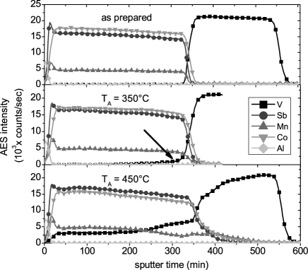
III.2 Inter-diffusion of Co-Mn-Sb and V: Auger depth profiling
The decrease of the magnetic moment above the optimal annealing temperature is caused by inter-diffusion of the Co-Mn-Sb layer with the V buffer. This is identified by Auger depth profilingSchmalhorst et al. (2002); Briggs and Seah (1990) of sample Half BI samples in the as prepared state and after annealing at 350∘C and 450∘C (Figure 2). The different layers are well separated in the as prepared state. The apparent maximum of the Mn intensity just below the barrier is caused by preferential sputtering of Manganese. It is a very common artifact of sputter depth profilingBriggs and Seah (1990) and was also found for Antimony. After annealing at 350∘C the depth profile is slightly changed, a small fraction of Vanadium could be detected in the lower part of the Co-Mn-Sb layer (see arrow in Figure 2). This inter-diffusion intensifies with increasing annealing temperature. Therefore the annealing temperature for samples Half A, Half CII and FullII was generally set to 350∘C to minimize diffusion.
In addition Auger depth profiles were taken for the Co rich samples Half BIII. After annealing at 450∘C the V concentration in the depth region of the Co-Mn-Sb layer was a factor of two smaller for sample Half BIII compared to sample Half BI, i.e. the inter-diffusion at the Co-Mn-Sb / V interface is considerably smaller for the off-stoichiometric samples. This indicates that the number of vacancy sites via which bulk diffusion can easily occur in Co-Mn-Sb decreases with increasing Co concentration.
III.3 Element-specific magnetic moments: X-ray absorption spectroscopy (XAS) and magnetic circular dichroism (XMCD)
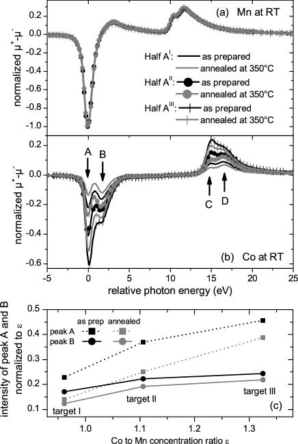
Temperature dependent x-ray absorption spectroscopy (XAS) and x-ray magnetic circular dichroism (XMCD) was performed at BL 6.3.1 of the Advanced Light Source in Berkeley, CA. The element-specific magnetic bulk properties were investigated at the Co- and Mn- edges in bulk-sensitive transmission modeIdzerda et al. (1994) on Half A samples in the as-prepared state and after annealing at 350∘C. The x-rays angle of incidence with respect to the sample surface was =45∘. The XMCD spectra were obtained by applying a magnetic field of 0.2 T along the x-ray beam direction using elliptically polarized radiation with a polarization of =+75%. and denote the linear absorption coefficients for parallel and anti-parallel orientation of photon spin and magnetic field. The transmitted x-rays were detected by a photo-diode. In conventional sum rule analysisChen et al. (1995) the number of holes needs to be taken from band structure calculations to calculate element-specific spin and orbital magnetic moments. Here, we follow the approach by Stöhr et al.Stöhr (1995) which bases on the assumption that the transition matrix elements connecting core and valence states are known and can be taken from other experiments. Details of our sum rule analysis procedure are given elsewhere Schmalhorst et al. (2009).
The XMCD spectra are shown in Fig. 3a and b, the extracted magnetic moment ratios are summarized in Tab. 3.
| target | ||||
|---|---|---|---|---|
| I | as prep. | |||
| 350∘C | ||||
| II | as prep. | |||
| 350∘C | ||||
| III | as prep. | |||
| 350∘C |
The shape of the Mn XMCD asymmetry is nearly the same for all samples and very similar to Mn in the full Heusler compound Co2MnSiSchmalhorst et al. (2004). Accordingly, the Mn orbital to spin moment ratio does not depend on layer composition or post-annealing. The small Mn orbital moments are typically -6% of the spin moments, i.e. both are aligned anti-parallel. Furthermore, the Mn magnetic moment of sample Half AI was found to be reduced by between 15 K and RT, which is in fair agreement with the data by Otto et al.Otto et al. (1987), who observed a reduction of the saturation magnetization for bulk samples of between K and RT and a Curie temperature of 478 K.
The Co spin moment is aligned in parallel to its small orbital moment and the target composition and the post-annealing has a significant influence on the Co to Mn spin magnetic moments ratio which can be directly seen from the different sizes of the normalized Co XMCD signals in Fig. 3 b. Two clear trends are observed: First, the normalized Co XMCD signal and, therefore, the relative contribution of each Co atom to the total magnetic moment of the samples is reduced by annealing for all samples of type Half A. Second, the relative contribution of the Co magnetic moments to the total magnetic moment of the samples increases with increasing Co concentration in the films. The smallest spin magnetic moment ratio of 18.8% is found for the annealed sample deposited from target I while the largest one (45.5%) is found for the as prepared sample deposited from target III (see Tab. 3). Similar results were found for annealed Co-Mn-Sb films grown on Cu/Ta/V buffers and are published elsewhereSchmalhorst et al. (2009).
Moreover, there is a remarkable double peak structure of the Co XMCD spectra at the and edge, which is significantly different from Co metalChen et al. (1995) or Co2MnSiSchmalhorst et al. (2004) and leads to a strongly changed electronic structure of the unoccupied Co states compared to the references. This structure changes with different film composition and post-annealing. In addition to the decrease of the Co to Mn spin moment ratio, which corresponds to generally reduced intensities of the peaks ”A” and ”B” (Fig. 3c), the intensity of peak ”A” is reduced further in comparison to ”B” with decreasing Co concentration and by annealing. The same holds for the corresponding peaks ”C” and ”D” at the edge. The changed shape of the Co XMCD spectra could be caused by a different degree of location of the 3d statesTelling et al. (2008) or hint to two non-equivalent Co positions in the Co-Mn-Sb crystal lattice. This is in accordance with the structural model of alternating Co2MnSb and MnSb structural units as discussed below. Moreover, because of the strong influence of the Co concentration on the spectral shape it is likely to assume, that the additional Co occupies the vacancy sites in the MnSb structural units.
The generally observed ferromagnetic coupling of the Mn and Co spin moment is important with respect to the different crystal structures discussed in the literature (see Sec. I). In the case of a C1b lattice an anti-ferromagnetic coupling of Co and Mn spin moments is expected (). For the more complex structures resulting in a very narrow or even vanishing spin-down gap, both moments are expected to be ferromagnetically coupled (Senateur’s model: Tobola and Pierre (2000); disordered structure: Kaczmarska et al. (1999); alternation of Co2MnSb and MnSb structural units: Ksenofotov et al. (2006)). Further, for CoMnSb crystallized in the C1b structure a parallel alignment of the spin and orbital moments is expectedGalanakis (2005). Obviously, our experimental data for the annealed Half AI sample fits best together with the structural model proposed by Ksenofontov et al.Ksenofotov et al. (2006).
By comparing the element-specific results and the bulk magnetization discussed in Sec. III.1 one can conclude that the general increase of the magnetization with increasing Co content (see Fig. 1) results from the larger Co content and the larger contribution of each Co atom to the total magnetic moment. The general reduction of after annealing and the simultaneous increase of the bulk magnetization means, that the atomic order is improved by the post-annealing process: the magnetization of CoMnSb crystallized in one of the three complex structures suggested by Tobola et al.Tobola and Pierre (2000), Kaczmarska et al.Kaczmarska et al. (1999) and Ksenofontov et al.Ksenofotov et al. (2006), respectively, is dominated by the Mn spin moment, which is aligned in parallel to the Co spin moment. Thereby, the Co magnetic moment is considerably smaller in these compounds compared to pure Co metal (Chen et al. (1995)), where nearest-neighbor Co atoms couple ferromagnetically. From this one would expect an increase of the mean Co magnetic moment per atom in case of atomic disorder, e.g., when Co atoms occupy Mn lattice sites. On the other hand, nearest-neighbor Mn atoms tend to couple antiferromagnetically, accordingly a decrease of the mean Mn magnetic moment would be expected for a disordered compound. This behavior has been predicted by Picozzi et al. for defects in ordered Co2MnSiPicozzi et al. (2004). Accordingly, the results can be explained as an improvement of the atomic order by the post-annealing process. A similar behavior has been observed for full Heusler compound thin films and multilayers like Co2MnSiSchmalhorst et al. (2004), Co2FeSi and Co2MnSi / Co2FeSiEbke et al. (2006); Schmalhorst et al. (2007b).
III.4 Crystal structure: X-ray diffraction (XRD)
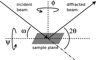
A Phillips X’Pert Pro MPD diffractometer equipped with an open Eulerian cradle and a copper anode was used for non-specular x-ray diffraction. Figure 4 displays the scattering geometry and the angle definitions. Crystallinity and atomic order of Co-Mn-Sb was studied and related to the magnetic and electronic properties.
Rocking curves and pole figures were taken to characterize the texture of the V buffer and the Co-Mn-Sb. Both materials grow (110) textured. The full width at half maximum (FWHM) of the Co-Mn-Sb (440)/(220) rocking curves is 8 for sample Half BI and 10 for sample Half BIII.
In textured samples, only one group of diffraction peaks is accessible with - scans. One can find that the (220) peak intensity of Heusler compounds is independent of site-swap disorderWebster (1969) by an analysis of the structure factors of a C1b (half) or L21 (full-)Heusler compound. In contrast, the (200) and (111) peak intensities depend on disorder and will vanish for A1 type disorder, where the lattice sites are randomly occupied. Therefore a (110)-textured L21 film will give the same specular diffractogram as a (110)-textured A1-disordered film of the same compound. Furthermore, this is also true for the various crystal structures which have been proposed for CoMnSb (see Sec. I).

To overcome this problem, non-specular - scans were taken with various settings of and . Figure 5 presents a set of these scans taken on sample Half BI (400∘C). The scan with shows the V (110) reflex and the strong (440) reflex from the Co-Mn-Sb. At higher values of more reflections appear. A well-ordered C1b lattice would exhibit the (222), (400) and (440) reflections only (which would be indexed (111), (200) and (220) then). The additional (311), (331), (333)/(511) and (531) peaks have comparatively low intensity and grow with increasing annealing temperature. Similar patterns were found by Ksenofontov et al.Ksenofotov et al. (2006) in powders of Co-Mn-Sb. The peaks can not be indexed based on a L21/C1b structure with a lattice constant of about 5.9 Å. In contrast, they can be indexed by the assumption of a doubled unit cell parameter of 11.77 Å.
Analogous measurements on sample Half BIII did not show the additional peaks. The complex unit cell with a doubled lattice constant is obviously specific for the nearly stoichiometric CoMnSb. The Co excess in films sputtered from target III might lead to occupation of the vacant sites in the MnSb substructure of the Co2MnSb-MnSb super cells. If finally one Co atom per f.u. is added (without reducing the Sb concentration at the same time), the system will be in the structure.
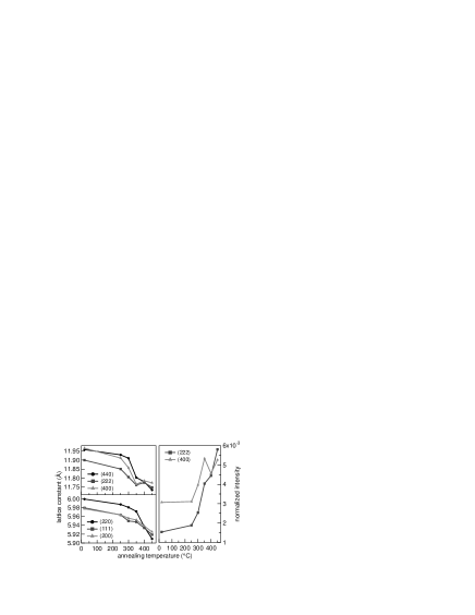
In Figure 6 we determine the in-plane and out-of-plane lattice parameters as a function of the annealing temperature for sample Half BI and sample Half BIII. The lattice parameters shrink with increasing annealing temperature, indicating a lattice relaxation and/or ordering. After 400∘C the lattice parameters in the three probed directions are the same, stress-induced influences might be compensated.
The integrated intensity of the (222) and (400) reflexes is a measure for the order in the films. Figure 6 (right) shows a plot of the normalized integrated (222) and (400) peak intensities as a function of the annealing temperature. The normalization is done with respect to the integrated (440) intensity to correct for recrystallization. The (222) intensity increases by a factor of 4 from the as-prepared sample to 450∘C. Note that the intensity of the (222) reflex is further increased with annealing from 400∘C to 450∘C, whereas the (400) reflex intensity does not increase monotonously, but rather shows a dip at =400∘C.
The additional peaks of the CoMnSb superstructure vanish for annealing at =450∘C. Vanadium is implemented into the lattice and thus decreases the saturation magnetization (Section III.1). The dip in the normalized (400) intensity curve at 400∘C hints the incipient diffusion of V, changing the properties of the lattice. However, the face-centered cubic structure is preserved and the V increases the structure factor of the (222) reflex.
IV The Co-Mn-Sb / Al-O interface
IV.1 X-ray absorption spectroscopy (XAS)
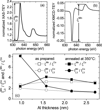
The influence of the Al thickness and the annealing on the chemical states of Co and Mn at the Co-Mn-Sb / Al-O interface was investigated by surface-sensitive XAS and XMCD in total electron yield (TEY) mode applied to Half CII samples, involving a plasma oxidized wedge of Al on top of Co-Mn-Sb. The Co-Mn-Sb/Al-O interface needs to be optimized with respect to the oxidation process of the Aluminum in order to reach maximum TMR ratios Schmalhorst et al. (2005b); Sacher ; Schmalhorst et al. (2007b).
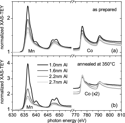
An increasing Mn to Co concentration ratio was found at the interface with decreasing Al thickness (see in Fig. 7c). This trend becomes more pronounced after annealing. The shapes of the Mn XA spectra in Figure 8 show that this Mn segregation at the Co-Mn-Sb/Al-O interface is caused by MnO formation at the lower barrier interface. For an Al thickness of only 1.0 nm the spectra of the as prepared as well as the annealed samples were dominated by the multiplet structure typical for MnOYonamoto et al. (2001). The multiplet structure became weaker with increasing Al thickness. A structureless absorption edge was found for thick Aluminum, its shape is similar to metallic bulk MnYonamoto et al. (2001).
The significant formation of interfacial MnO (paramagnetic at room temperaturePepy (1974)) for 1.0 nm thick Al is also reflected in the low XMCD asymmetry ratio . This is proportional to the ratio of the Mn and Co magnetic moments, which are both dominated by the spin moment (see above). was maximal after annealing for an Al thickness of 1.6 nm and the contribution of MnO to the XA spectrum is already very small compared to 1.0 nm Al (see Figure 8b). Here, the best atomic order was achieved, since disorder is expected to reduce the Mn to Co magnetic moment ratio (see Sec. III.3). While thin Al leads to an oxidation of the ferromagnetic electrode, metallic Al will remain at the interface, if the Al thickness is too large. This Al can diffuse into the Co-Mn-Sb electrode during annealing leading to a reduction of the interfacial magnetic moments and the Mn to Co magnetic moment ratio. The observed increase of the Mn to Co (bulk) spin moment ratio of all films discussed in the previous Sec. III.3 was not found at the Co-Mn-Sb/Al-O interface for 2.7 nm thick Al due to residual unoxidized Al. However, such an increase was found for optimum aluminum thickness of 1.6 nm. At this Al thickness, the properties of the Co-Mn-Sb near the surface are closest to those of the bulk material.
IV.2 Transport properties of magnetic tunnel junctions with Co-Mn-Sb electrode
The magnetic tunnel junctions FullII were prepared with optimized growth conditions as discussed earlier: they were in-situ annealed at 350∘C after 150 s plasma-oxidation of the Al wedge. In order to remove contaminations from the surface, the samples were plasma oxidized for another 50 s after the annealing. Subsequently, ex-situ vacuum annealing at 275∘C in a magnetic field of 0.1 T was employed to set the exchange bias of the pinned electrode. In previous papersKämmerer et al. (2001); Ebke et al. (2006) we show that this preparation scheme is suitable to produce magnetic tunnel junctions with Heusler compound electrodes that exhibit high TMR ratios. Patterning was done by optical lithography and ion beam etching, the transport properties of the quadratic 100 100 m2 wide MTJs were measured by conventional two-probe method with a constant dc bias voltage.

In Figure 9 the dependence of the TMR on the Al thickness is shown. A maximal TMR ratio of 8.5% at room temperature was found at an Al thickness of 1.25 nm (1.6 nm AlOx). The Al thickness dependence of presented in the last section fits quite well to the Al thickness dependence of the TMR. The observed maximum TMR ratio at 13 K was 24% (see inset in Figure 9). According to the Jullière model, the effective tunneling spin polarization is calculated to be 0.22, using a spin polarization for Co70Fe30 of 0.5 Thomas (2003). No higher values for the TMR ratio could be found with varied film growth parameters. Moreover, MTJs with Co-Mn-Sb electrodes from targets I and III show comparable TMR ratios. Taking this together with the careful preparation of the films and the tunnel barrier, we conclude that the low observed spin polarization is an intrinsic property of our Co-Mn-Sb electrodes.
V Conclusion
It was shown that post annealing increases the atomic order and the magnetization of the Co-Mn-Sb films, while the Co to Mn magnetic moment ratio decreased. The samples degraded for temperatures higher than 350∘C because of inter-diffusion of V at the Co-Mn-Sb / V interface. Adding Co to the samples leads to higher magnetization values and to a larger Co to Mn magnetic moment ratio as expected from simple arguments basing on the typical nearest-neighbor coupling behavior of Co-Co and Mn-Mn pairs. A parallel coupling of the Co and Mn magnetic spin moments was found for all compositions. For nearly stoichiometric films the Co to Mn spin moment ratio was +18.8% after annealing and the unit cell parameter was 11.77 Å. This fits the expectations for CoMnSb crystallized in a complex Co2MnSb/MnSb super structure as reported by Ksenofontov et al.Ksenofotov et al. (2006). The addition of Co as well as interdiffusion from the vanadium buffer destroy the super structure. Finally, the transport properties of magnetic tunnel junctions with Co-Mn-Sb electrode, Al-O barrier and Co-Fe counter electrode are in agreement with the predicted low spin polarization: we found an effective tunneling spin polarization of only 22%, which clearly indicates a non-half metallic character of CoMnSb.
Acknowledgement
The authors gratefully acknowledge financial support by the Deutsche Forschungsgemeinschaft (DFG) and the Deutscher Akademischer Austausch Dienst (DAAD) and the opportunity to work at BL 6.3.1 of the Advanced Light Source, Berkeley, USA. The ALS is supported by the U.S. Department of Energy under Contract No. DE-AC02-05CH11231. For financial support of the XRD measurements under contract No.DAAD/10/2006 M.M., T.S. and J.K. gratefully acknowledge the Ministry of Science and Higher Education of Poland.
References
- Wolf et al. (2001) S. A. Wolf, D. D. Awschalom, R. A. Buhrman, J. M. Daughton, S. von Molnar, M. L. Roukes, A. Y. Chtchelkanova, and D. M. Treger, Science 294, 1488 (2001).
- Reiss and Meyners (2006) G. Reiss and D. Meyners, Appl. Phys. Lett. 88, 043505 (2006).
- Thomas et al. (2006) A. Thomas, D. Meyners, D. Ebke, N. Liu, M. D. Sacher, J. Schmalhorst, G. Reiss, H. Ebert, and A. Hütten, Appl. Phys. Lett. 89, 012502 (2006).
- Julliere (1975) M. Julliere, Phys. Lett. 54A, 225 (1975).
- de Groot et al. (1983) R.A. de Groot, F.M. Mueller, P.G. vanEngen, and K.H.J. Buschow, Phys. Rev. Lett. 50, 2024 (1983).
- Ishida et al. (1998) S. Ishida, T. Masaki, S. Fujii, and S. Asano, Physica B 245, 1 (1998).
- Galanakis et al. (2002) I. Galanakis, P. H. Dederichs, and N. Papanikolaou, Phys. Rev. B 66, 174429 (2002).
- Wurmehl et al. (2005) S. Wurmehl, G.H. Fecher, H. C. Kandpal, V. Ksenofontov, C. Felser, H.-J. Lin, and J. Morais, Phys. Rev. B 72, 184434 (2005).
- (9) Half-metallic Alloys: Fundamentals and Application, I. Galanakis and P. H. Dedrichs (Eds.), Lecture Notes in Physics 676, Springer Berlin Heidelberg (2005), ISBN-10 3-540-27719-6.
- Inomata et al. (2004) K. Inomata, N. Tezuka, S. Okamura, H. Kobayashi, and A. Hirohata, J. Appl. Phys. 95, 7234 (2004).
- Schmalhorst et al. (2005a) J. Schmalhorst, S. Kämmerer, G. Reiss, and A. Hütten, Appl. Phys. Lett. 86, 052501 (2005a).
- Oogane et al. (2006) M. Oogane, Y. Sakuraba, J. Nakata, H. Kubota, Y. Ando, A. Sakuma, and T. Miyazaki, J. Phys. D: Appl. Phys. 39, 834 (2006).
- Ebke et al. (2006) D. Ebke, J. Schmalhorst, N.-N. Liu, A. Thomas, G. Reiss, and A. Hütten, Appl. Phys. Lett. 89, 162506 (2006).
- Sakuraba et al. (2006) Y. Sakuraba, M. Hattori, M. Oogane, Y. Ando, H. Kato, A. Sakuma, T. Miyazaki, and H. Kubota, Appl. Phys. Lett. 88, 192508 (2006).
- Schmalhorst et al. (2007a) J. Schmalhorst, A. Thomas, S. Kämmerer, O. Schebaum, D. Ebke, M. D. Sacher, G. Reiss, A. Hütten, A. Turchanin, A. Gölzhäuser, et al., Phys. Rev. B 75, 014403 (2007a).
- Schmalhorst et al. (2008) J. Schmalhorst, D. Ebke, A. Weddemann, A. Hütten, A. Thomas, G. Reiss, A. Turchanin, A. Gölzhäuser, B. Balke, C. Felser, J. Appl. Phys. 104, 043918 (2008a).
- Tanaka et al. (1999) C. T. Tanaka, J. Nowak, and J. S. Moodera, J. Appl. Phys. 86, 6239 (1999).
- Ishikawa et al. (2008) T. Ishikawa, S. Hakamata, K. Matsuda, T. Uemura, and M. Yamamoto, J. Appl. Phys. 103, 07A919 (2008).
- Ikeda et al. (2008) S. Ikeda, J. Hayakawa, Y. Ashizawa, Y. M. Lee, K. Miura, H. Hasegawa, M. Tsunoda, F. Matsukura, and H. Ohno, Appl. Phys. Lett. 93, 082508 (2008).
- Galanakis (2002) I. Galanakis, J. Phys.: Condens. Matter 14, 6329 (2002).
- Otto et al. (1987) M. J. Otto, H. Feil, R. A. M. van Woerden, J. Wijngaard, P. J. van der Valk, C. F. van Bruggen, and C. Haas, J. Magn. Magn. Mat. 70, 33 (1987).
- Tobola and Pierre (2000) J. Tobola and J. Pierre, J. Alloys and Compd. 296, 243 (2000).
- Senateur et al. (1972) J. P. Senateur, A. Rouault, R. Fruchart, and D. Fruchart, J. Solid State Chem. 5, 226 (1972).
- Kaczmarska et al. (1999) K. Kaczmarska, J. Pierre, J. Tobola, and R. V. Skolozdra, Phys. Rev. B 60, 373 (1999).
- Ksenofotov et al. (2006) V. Ksenofontov, G. Melnyk, M. Wojcik, S. Wurmehl, K. Kroth, S. Reiman, P. Blaha, and C. Felser, Phys. Rev. B 74, 134426 (2006).
- Schmalhorst et al. (2002) J. Schmalhorst, H. Brückl, G. Reiss, G. Gieres, and J. Wecker, Journal of Appl. Physics 91, 6617 (2002).
- Briggs and Seah (1990) D. Briggs and M. P. Seah, Practical Surface Analysis, Chapter 4: Depth profiling in AES and XPS (John Wiley & Sons, 1990).
- (28) The depth resolution of the profiles can be calculated from the slope of the V intensity at the V / SiO2 interfaceBriggs and Seah (1990). The slope is very similar for the as prepared and the 450∘C samples, the sputter time needed to reduce the intensity from 84% to 16% of the maximum V intensity is 20.7min (as prepared) and 20.4min (450∘C), respectively. By comparing these sputter times with the required 214min to sputter through the 40nm thick V layer of the as prepared sample an identical depth resolution of about 4nm can be estimated for all three samples.
- Idzerda et al. (1994) Y. U. Idzerda, C. T. Chen, H.-J. Lin, G. Meigs, G. H. Ho, and C.-C. Kao, Nucl. Instrum. Methods Phys. Res. A 347, 134 (1994).
- Chen et al. (1995) C. T. Chen, Y. U. Idzerda, H.-J. Lin, N. V. Smith, G. Meigs, E. Chaban, G. H. Ho, E. Pellegrin, and F. Sette, Phys. Rev. Lett. 75, 152 (1995).
- Stöhr (1995) J. Stöhr, J. Elect. Spect. Rel. Phen. 75, 253 (1995).
- Schmalhorst et al. (2009) J. Schmalhorst, D. Ebke, M. Meinert, A. Thomas, G. Reiss, and E. Arenholz, J. Appl. Phys. 105, 053906 (2009).
- Schmalhorst et al. (2004) J. Schmalhorst, S. Kämmerer, M. Sacher, G. Reiss, A. Hütten, and A. Scholl, Phys. Rev. B 70, 024426 (2004).
- Telling et al. (2008) N. D. Telling, P. Keatley, G. van der Laan, R. J. Hicken, E. Arenholz, Y. Sakuraba, M. Oogane, Y. Ando, K. Takanashi, A. Sakuma, et al., Phys. Rev. B 78, 184438 (2008).
- Galanakis (2005) I. Galanakis, Phys. Rev. B 71, 012413 (2005).
- Picozzi et al. (2004) S. Picozzi, A. Continenza, and A. J. Freeman, Phys. Rev. B 69, 094423 (2004).
- Schmalhorst et al. (2007b) J. Schmalhorst, D. Ebke, M. D. Sacher, N.-N. Liu, A. Thomas, G. Reiss, and A. H. E. Arenholz, IEEE Trans. Magn. 64, 2806 (2007b).
- Webster (1969) P. Webster, Contemp. Phys. 10, 559 (1969).
- Schmalhorst et al. (2005b) J. Schmalhorst, M. D. Sacher, A. Thomas, H. Brückl, G. Reiss, and K. Starke, J. Appl. Phys. 97, 123711 (2005b).
- (40) M. D. Sacher, PhD Thesis, Bielefeld University, Germany (2008).
- Yonamoto et al. (2001) Y. Yonamoto, T. Yokoyama, K. Amemiya, D. Matsumura, and T. Ohta, Phys. Rev. B 63, 214406 (2001).
- Pepy (1974) G. Pepy, J. Phys. Chem. Solids 35, 433 (1974).
- Kämmerer et al. (2001) S. Kämmerer, A. Thomas, A. Hütten, G. Reiss, Appl. Phys. Lett. 85, 79 (2004).
- Thomas (2003) A. Thomas, Ph.D. thesis, University of Bielefeld (2003).