Interface Trap Density Metrology of state-of-the-art undoped Si n-FinFETs
Abstract
The presence of interface states at the MOS interface is a well-known cause of device degradation. This is particularly true for ultra-scaled FinFET geometries where the presence of a few traps can strongly influence device behavior. Typical methods for interface trap density () measurements are not performed on ultimate devices, but on custom designed structures. We present the first set of methods that allow direct estimation of in state-of-the-art FinFETs, addressing a critical industry need.
I Introduction
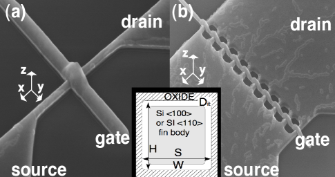
Non-planar trigated FinFET geometry (Fig. 1a, b) provides a viable solution to the channel length () scaling due to their better gate to channel electrostatic coupling and reduced Short Channel Effects (SCEs) Won133 . In a recent work Tet150 , it has been demonstrated that by using thermionic emission, it is possible to measure (1) the active channel cross-section area () (inset Fig. 1), which represents the portion of the physical cross-section of channel where the charge flows, and (2) the source to channel barrier height (), which reflects on the ease with which electrons travel from the source (drain) to the channel, hence opening new ways to investigate FinFETs. Furthermore, it was found that, although the trends of in the experimental and the simulated data were identical, differences in the absolute values were observed. These differences were found to be caused by the presence of interface states at the metal-oxide-semiconductor interface of the experimental devices Tet150 ; Lee186 . These states can trap electrons and enhance the presence of screening, therefore reducing the action of the gate on the channel, and as a final result, a decrease in the absolute value of in the experimental data is observed. Here we show that, by using simple mathematical manipulations and the difference between experimental and simulated values of and of the capacitive coupling Tet150 , it is possible to infer the interface trap density (). Typical measurements are not performed on ultimate devices but on custom designed structures Kap232 . Such custom structures may only be partially reflective for the possibly surface orientation-dependent and geometry-dependent . Here, we provide a simple set of methods for the direct estimation of in ultimate devices. The comparison between the values of obtained with our two methods and between our results and the results obtained using a method implemented in the past Kap232 show similar trend. A new approach to trap density metrology is of critical importance as CMOS scaling leads device dimensions into nanometer regime. At these scales, quantities such as can vary rapidly with device geometry, rendering old techniques inadequate as they cannot be applied directly in these ultra-scaled devices.
| FinFET label | W(nm) | H(nm) | L(nm) | Number of channels | Channel orientation | anneal |
|---|---|---|---|---|---|---|
| A | 25 | 65 | 40 | Yes | ||
| B | 25 | 65 | 40 | No | ||
| C | 5 | 65 | 40 | No | ||
| D and E | 18 | 40 | 40 | Yes | ||
| F | 3-5 | 40 | 40 | Yes |
II Device and experimental details
The undoped n-FinFETs used in this work (, see table 1) consist of nanowire channels etched on a Si intrinsic film with a wrap-around gate covering three faces of the channels (Fig. 1) Col108 . An HfSiO layer isolates a TiN layer from the intrinsic Si channel Col108 . Devices with the same channel length, ( = 40 nm), different channel height ( = 40 nm and 65 nm), different channel widths (3 nm 25 nm), 100 or 110 channel orientation and different surface treatment ( with hydrogen anneal step during fabrication Lee186 and without) have been studied. Differential conductance () data are taken at = using a lock-in technique. The complete experimental procedure to extract and can be found in Ref. Tet150 .
III Modeling Approach
To obtain the self-consistent charge and potential in n-FinFETs, the electronic structure is calculated using an atomistic 10 band semi-empirical Tight-Binding (TB) Kli601 ; Boy115201 , which captures the geometrical and potential confinement, takes into account the atomic positions in the device Kli601 ; Boy115201 ; Neo1286 , and is coupled self-consistently to a Poisson solver Neo1286 ; Paul1 . The thermionic current in the FinFETs is obtained using a ballistic top-of-the-barrier (ToB) model Neo1286 ; Paul1 . Due to the extensively large cross-section of the devices that combines up to 44,192 atoms (for = 65 nm, = 25 nm FinFETs) in the simulation domain, a new NEMO 3D code has been integrated in the top of the barrier analysis Sunhee1 . Using thermionic fitting procedure Tet150 , , and can be extracted using the experimental and theoretical conductance () in the thermionic emission regime for a 3D system sze1 as,
| (1) |
where is the effective 3D Richardson constant (), is the temperature, is the Boltzmann constant and e is the electronic charge. This will hold only when the cross-section size of the FinFET is large enough (i.e.: , 20 nm) to be considered a 3D bulk system. In this study, is extracted for FinFETs with W(H) 25 nm (65 nm). When the approximation is not true anymore (eg. or 20 nm), only and can be correctly extrapolated Tet150 .
IV Results and Discussion
Two techniques to extract in n-Fin-FETs are presented.
IV.1 Method I
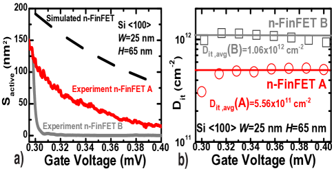
The active cross-section in the undoped n-FinFETs is extracted from the temperature based conductance measurement using (1) as outlined in Ref. Tet150 . Theoretically is extracted for two n-FinFETs with W/H = 25 nm/65 nm ( and ) and the comparison of the simulated value of with experimental data is shown in Fig. 2a. The simulations overestimate the value of due to the electrostatic screening of the channel from the gate due the interface trap charges () present in these FinFETs Tet150 ; Kap232 . Based on the difference in the simulated and the experimental , values, a method to extract in the FinFET devices is outlined (see table 2). The method is based on the fact that the total charge in the channel at a given must be the same in the experiments and in the simulations. We therefore assume that the difference between the simulated () and the trap charge density () is equal to the experimental charge density () (see appendix). This leads to the following equation:
| (2) |
where is the perimeter of the channel under the gate (). The extracted ( ) with (for W/H = 25 nm/65 nm), based on (6), is shown in Fig. 2b. The value is almost constant with showing that all the traps are filled (and therefore justifying the assumption ). The average value of interface trap density is obtained as for device and for device (Fig. 2b). The values for compare quite well with the experimental values for two different devices from Ref.Kap232 (table 2). The validity of these results are also supported by the fact that the obtained interface trap density values are different for devices with different surface treatment, as it is well known that the hydrogen anneal step during fabrication greatly improves device characteristics and reduces the interface trap density Lee186 . As expected, for device we find much higher compare to device .
IV.2 Method II
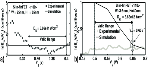
By assuming that the surface potential () and the respond equaly to Tet150 ; sze1 , a second extraction approach for is developed. Simple calculations (see sze1 and the appendix) result in an integrated trap charge density:
| (3) |
with =0.0173 ( is assumed to be the same for all the devices since the oxide thickness is the same in all the devices). This method depends on the valid range of the used for integration in Eq. (3). The limits are set from the point where 1 till the threshold voltage () of the FinFET (Fig. 3), after the flat-band shift () of the simulated curve. All the extracted from Method II are shown in table 2. In the calculation few assumptions were made; (1) the extra charge contribution is assumed to come completely from the interface trap charges () and any contribution from the bulk trap states have been neglected, (2) this method of extraction works best for undoped channels since any filling of impurity states is neglected in the calculations.
V Conclusion
A new determination methodology for state-of-the-art n-FinFETs is presented. Two complementary approaches provide (a) the gate bias () dependence of (Method I) and, (b) the total (Method II); both found consistent with each other. The following trends are observed; (i) devices fabricated without hydrogen annealing step, with smaller ’s and with 110 channel orientation show higher compared to the other devices, (ii) by comparison of the value of obtained for device in the two approaches (Fig. 2 and Fig. 3) and the value of obtained for two identical devices ( and ) using the same approach (Method II), compatibility and reproducibility of the methods are demonstrated. The reported trends are similar to the one suggested in the literature Lee186 .
| n-FinFET label | Approach | ( ) | FinFET type | Remarks |
|---|---|---|---|---|
| L=140nm Kap232 | Charge Pumping | 1.725 | Gated-diode FET Kap232 | |
| L=240nm Kap232 | Charge Pumping | 2.072 | Gated-diode FET Kap232 | |
| A | Method I | 5.560 | Standard FET | anneal, Low |
| B | Method I | 10.6 | Standard FET | No anneal, higher |
| B | Method II | 8.86 | Standard FET | No anneal, higher |
| C | Method II | 9.26 | Standard FET | Thin fin width, more etching, Higher |
| D (E) | Method II | 18.31 (15.3) | Standard FET | 110, higher bond density, Higher |
| F | Method II | 36.3 | Standard FET | Same as C+D, Much Higher |
VI Acknowledgements
G. C. Tettamanzi and S. Rogge are with the Delft University of Technology, 2628 CJ Delft, The Netherlands. A. Paul, S. Lee, S. R. Mehrotra and G. Klimeck are with the Network for Computational Nanotechnology and the School of Electrical and Computer Engineering, Purdue University, West Lafayette, IN-47906, USA. N. Collaert and S. Biesemans are with IMEC, 3001 Leuven, Belgium. G.C.T. and S.R. acknowledge FOM and the European Community Seventh Framework under the Grant Agreement nr: 214989-AFSiD for the financial support. A.P., S.L., S. R. M. and G.K acknowledge the financial support from SRC, FCRP-MSD and NSF. Computational resources provided by nanoHUB.org is also acknowledged. G.C.T. acknowledge the kind hospitality extended by Prof. A. Di Carlo at the University of Tor Vergata, Rome, during the preparation of this manuscript. *G.C.T. and A.P. contributed equally to this work. (Emails: giuseppe.tettamanzi@gmail.com, abhijeet.rama@gmail.com).
VII Appendix
As outlined in Ref. Tet150 , in undoped n-FinFETs the active channel cross-section area () and the source-to-channel barrier height () can be extracted from the temperature based conductance measurements. Furthermore, in these devices, the differences between the values of the experimental and the simulated and can be used for the extraction of interface traps density ().
In this appendix, the details about the extraction procedure of are outlined. The material is organized in the following sections. Interface trap extraction using difference in is outlined in Sec. VII.1 along with the assumptions. Section VII.2 outlines the procedure for extraction using the differences between experimental and simulated gate-to-channel coupling values () along with the assumptions. Conclusions are given in Sec. VII.3.
VII.1 Method I
Based on the difference between the simulated and the experimental active channel cross-section area values ( and respectively), a method to extract in FinFET devices is outlined.
As the total charge in the channel at a given must be the same in the experiments and in the simulations (charge neutrality), the following equation is obtained:
| (4) |
where is the channel length, P is the perimeter of the channel under the gate (P = as show in Fig. 1 of the main paper), is the width of the channel, is the height of the channel, () is the simulated (experimental) charge density, e is the electronic charge and the number of trap charges at the interface. Locally it can be assumed that can be obtained from and using Eq. (5):
| (5) |
| (6) |
from this, the interface trap density can be extrapolated using the approximation .
VII.1.1 Assumptions in Method I
In the calculation of () few assumptions were made. The extra charge contribution completely comes from the interface trap density () and any contribution from the bulk trap states have been neglected. Also all the interface traps are assumed to be completely filled which justifies the fact that we can assume that . This method of extraction works best for undoped channel since any filling of the impurity/dopant states is neglected in the calculation. Also the interface trap density is assumed to constant for top and side walls of the FinFET which is generally not the case Kap232 .
VII.2 Method II

Based on the difference between simulated and experimental value of , a second method for the extraction of has been demonstrated. Starting from the equivalent capacitance model for a MOSFET with and and without the interface traps, as shown in Figure 4, the basic idea comes from Eq.(38) on page 383 in Ref. sze1 which gives,
| (7) |
where and are the total and the oxide capacitance, respectively. For the two cases shown in Fig. 4 the total capacitance is given by,
| (8) | |||||
| (9) |
with being the depletion capacitance and the interface capacitance. Equation (8) and (9) represent the total capacitances in the experimental and in the simulated device under ideal condition without any interface traps, respectively.
| (10) |
where of course .
| (11) |
| (12) |
In Eq. (11) all the values are dependent on except . Integrating Eq. (12) with regard to the final expression for the integrated interface charge density in the FinFETs is,
| (13) |
where is the threshold voltage of the FinFET and is the at which . This is the integration range for Eq. (13) in the sub-threshold region.
VII.2.1 Assumptions in Method II
While deriving the final equation for method II some assumptions were made. The first most important assumption is that the rate of change of the surface potential () is same as with . The extra charge contribution completely comes from the interface trap density () and any contribution from the bulk trap states have been neglected. Also all the interface traps are assumed to be completely filled which means = . This method works best when the change in DC and AC signal is low enough such that the interface traps can follow the change sze1 .
VII.3 Conclusion
The detailed calculation for both the trap extraction methods have been provided along with the assumtions made to obtain the final equations. The important point to note here is that, method I provides the variation in interface trap charges with the gate bias however, method II provides the total interface trap charge density within a range of gate bias. The application and the results obtained from these methods are provided in the main paper.
References
- (1) H.-S. P. Wong, Beyond the conventional transistors, IBM J. Res. Dev 46, 133 (2002)
- (2) Tettamanzi, G.C. and Paul, A. and Lansbergen, G.P. and Verduijn, J. and Sunhee Lee and Collaert, N. and Biesemans, S. and Klimeck, G. and Rogge, S., Thermionic Emission as a Tool to Study Transport in Undoped nFinFETs, Electron Device Letters, IEEE 31, 150-152 (2010)
- (3) Jeong-Soo Lee and Yang-Kyu Choi and Daewon Ha and Balasubramanian, S. and Tsu-Jae King and Bokor, J., Hydrogen annealing effect on DC and low-frequency noise characteristics in CMOS FinFETs, Electron Device Letters, IEEE 24, 186-188 (2003)
- (4) Kapila, G. and Kaczer, B. and Nackaerts, A. and Collaert, N. and Groeseneken, G.V., Direct Measurement of Top and Sidewall Interface Trap Density in SOI FinFETs, Electron Device Letters, IEEE 28, 232-234 (2007)
- (5) N. Collaert and M. Demand and I. Ferain and J. Lisoni and Singanamalla and P. Zimmerman and Y.-S. Yim and T. Schram and G. Mannaert and M. Goodwin and J. C. Hooker and F. Neuilly and M. C. Kim and K. De Meyer and S. De Gent and W. Boullart and M. Jurczak and S. Biesemans, Tall Triple-Gate Devices with. TiN/HfO2 Gate Stack, Symp VLSI Tech. p. 108 (2005)
- (6) Gerhard Klimeck and Fabiano Oyafuso and Timothy B. Boykin and Robert C. Bowen and P. von Allmen, Development of a Nanoelectronic 3-D (NEMO 3-D) Simulator for Multimillion Atom Simulations and Its Application to Alloyed Quantum Dots, Computer Modeling in Engineering and Science (CMES) 5, 601-642 (2002)
- (7) Boykin, T. B. and Klimeck, G. and Oyafuso, F., Valence band effective-mass expressions in the empirical tight-binding model applied to a Si and Ge parameterization, Phys. Rev. B 69, 115201 (2004)
- (8) Neophytou, N. and Paul, A. and Lundstrom, M. and Klimeck, G., Bandstructure Effects in Silicon Nanowire Electron Transport, IEEE, Trans. on Elec. Dev. 55, 1286-1297 (2008)
- (9) Paul, A., Mehrotra, S., Luisier, M. Klimeck, G., On the validity of the top of the barrier quantum transport model for ballistic nanowire MOSFETs, 13th International Workshop on Computational Electronics (IWCE), DOI:10.1103/IWCE.2009.5091134 (2009)
- (10) Lee, S. and Ryu, H. and Jiang, Z. and Klimeck, G, Million Atom Electronic Structure and Device Calculations on Peta-Scale Computers, 13th International Workshop on Computational Electronics (IWCE), DOI:10.1109/IWCE.2009.5091117 (2009)
- (11) S. M. Sze, Physics of Semiconductor Devices, Wiley, New York, 1981