Large tunable photonic band gaps in nanostructured doped semiconductors
Abstract
A plasmonic nanostructure conceived with periodic layers of a doped semiconductor and passive semiconductor is shown to generate spontaneously surface plasmon polaritons thanks to its periodic nature. The nanostructure is demonstrated to behave as an effective material modeled by a simple dielectric function of ionic-crystal type, and possesses a fully tunable photonic band gap, with widths exceeding 50%, in the region extending from mid-infra-red to Tera-Hertz.
pacs:
42.25.Bs, 42.79.-e, 78.20.Ci Phys. Rev. B 82 (2010) 195301I Introduction
The science of surface plasma waves on metallic-dielectric interfaces Raether , has received such interest as to become a true branch of physics, the palsmonics, and opened new perspectives in the control of light-matter interactions, see e.g. Refs.Zayatsa ; Maier ; Bliokh . The surface plasmon polariton (SPP), which results from coupling electromagnetic field with collective oscillations of electrons supported by the metal/dielectric interface, has unique physical properties based on enhanced nanolocalized optical fields, allowed by the negative dielectric constant of the metal below the plasma frequency. For example SPP propagation can be controlled by waveguides Gramotnev or by plasmonic crystals whose metal film periodically nanostructured induces the plasmonic band gap Kitson ; Bozhevolnyi .
Engineering of surface plasmons using nanostructuration made it possible to develop a new range of materials with remarkable optical properties such as extraordinary optical transmission Ebbesen , optical filtering Collin , optical magnetism Temnov , second harmonic generation Pu or higher harmonic generation in extreme UV Kim , and also to control the optical processes at the femto-second scale Kekatpure ; Utikal . The main concern is to control the optical properties associated with surface plasmons by engineering effective materials through periodicity, size and metal shape of the nano-objects. For instance a recent theoretical study proposed the nanosturcturation of metallic nano-sticks along the three direction of space to highlight a strong coupling between the incident light and the free electrons of the metal which opens a photonic band gap (with a stop band of 6.3%) in the telecom wavelength range Huang .
The main idea is to ensure opening of the gap by using the polaritonic nature of surface plasmons rather than Bragg reflections. As a matter of fact, the dispersion relation of an electromagnetic wave propagating along the interface between a metal and a dielectric, the so-called surface wave, is similar to the one resulting from a strong coupling between a photon and an oscillator, it is said to be ionic-crystal-like Raether . However, while the low energy surface plasmon branch is purely two-dimensional, the high energy branch of the dispersion relation is radiative and therefore a photon propagating along the interface will not see the stop band. Studies of such systems dates back to 1969 Economou , revealing three branches in the SPP dispersion relation, two of them corresponding to the anti-symmetric modes, the third one to the symmetric modes.
We study light propagation in a periodic nanostructure constituted of planar layers of a metal and a dielectric, sketched in Fig.1, assumed infinitely periodic and infinite in the second transverse direction. We demonstrate that this metal-dielectric nanostructure, worked as a planar waveguide array, but outside the guided mode regime, naturally and spontaneously generates SPP and then behaves as an effective three-dimensional material whose optical properties are completely and precisely understood by means of a single effective dielectric function of the ionic-crystal type, the formula (2) below.
Moreover, using, instead of a metal, a doped semiconductor is a means, by adapting the doping level, to set the plasma frequency in a chosen range, such as, in particular, to avoid absorption due to interband transitions. Then the simplicity of the obtained effective dielectric function allows one to determine readily how the choice of the materials and the dimensions of the nanostructure will tune the width of the stop band, and how the doping level will tune its position. The properties of the effective material in the gap region is the principal concern of our study with future interest in its switching properties in nonlinear regimes, see e.g. Refs.Porto ; Wurtz .
We thus demonstrate the polariton nature of the system when it is worked with transverse magnetic (TM) fields, in the long-wave approximation. Similar studies in literature focus mainly on the SPP properties of metal-dielectric structures, looking thus at the lower branch of the dispersion curve. Our approach predicts the behavior of the system on the entire spectrum, namely the lower polariton branch, the stop band and the upper polariton branch. Last we show that the approach applies as well for transverse electric (TE) fields. The structure works then as a simple metal for which we compute explicitly the high frequency dielectric constant and the (tunable) plasma effective frequency.
II Main result
From now on, all frequencies are normalized to the plasma frequency the wave numbers to , the lengths to (including spatial variables) and time to . Moreover we name frequency the actual angular frequency, units , and all dielectric constants are the relative ones. The doped semiconductor working as a metal, we use a Drude model with optical index and thus the final index profile of the periodic array can be written in the elementary cell as
| (1) |
The damping coefficient is also dimensionless and scaled to .
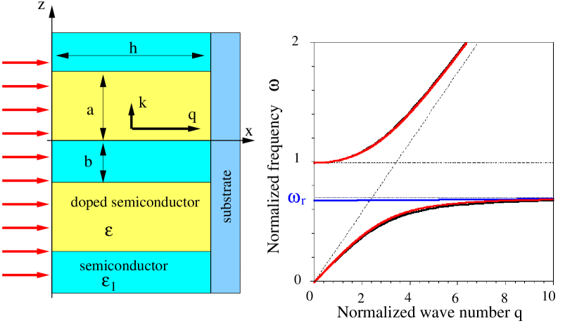
We shall demonstrate that, under TM irradiation, in the long wave limit, the resulting metamaterial is equivalent to a single layer having the following effective dielectric function
| (2) |
with the resonant dimensionless eigenfrequency and high frequency dielectric constant given by
| (3) |
Eq.(2) is identical to the dielectric function of an ionic crystal with relative high frequency dielectric constant , characteristic transverse frequency , and longitudinal frequency (by normalization). As a matter of fact, Fig.1 displays an example of the exact dispersion relation for the anti-symmetric modes (red curves) compared to the ionic crystal dispersion law (plotted with as black curves). The blue curve corresponds to the symmetric modes as explained in Sec.IV.
III Simulations
We perform numerical simulations of a realistic system submitted to TM normal incidence and calculate the reflection and transmission coefficients. The presented spectra are simulated with the commercial software package running finite difference time domain FDTD . We shall illustrate our task by using InAs for both semiconductors (high-frequency dielectric constants ), doping with silicon (Si) at a density of that produces a plasma frequency and hence plasma . The dimensions of the nanostructure and the damping factor are taken as
| (4) |
which means normalized quantities , and .
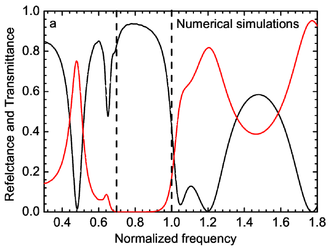
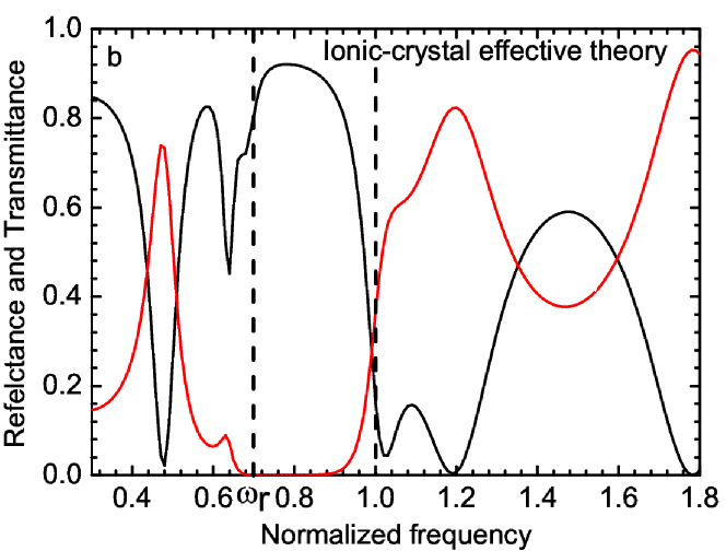
Fig.2 shows the result of a simulation where transmittance and reflectance are plotted in terms of the frequency of the incident TM plane wave at normal incidence. It is then quite remarkable that the spectra are almost identical, which evidences our main claim, though Fig.2b has been obtained with two major approximations: the ionic-crystal dielectric function (2) and the effective layer modelization.
The obtained normalized stop band can then be easily broadened by playing with the dimensions of the nanostructure, the plasma frequency , and the materials. For example changing the passive semiconductor from InAs to GaSb (dielectric constant ) increases the stop band from 29% to 33% for a depth . Last, in order to confirm that the stop band is not the result of a Bragg scattering, we made a series of simulations with an incident angle varying from 0 to 15 degrees, and with layer thicknesses up to , without any noticeable change in the spectra.
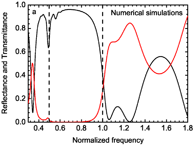
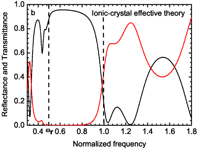
Another example is displayed in Fig.3 where we have modified only the geometry of the structure by increasing the width of the doped semiconductor to and reducing the width of the passive semiconductor to . The size of the stop band then reaches 50% of . Small discrepancies appear in the lower end of the spectrum, related to the long-wave approximation which, in the cases , is less accurate. We found that the lower branch of the dispersion relation (12) is for less close to the actual branch given by the solution of (10).
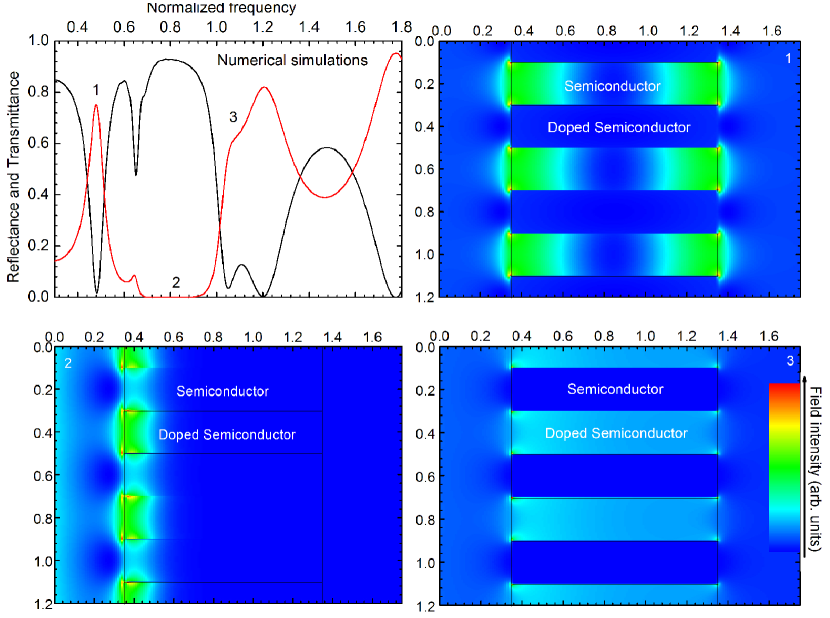
It is now worth understanding the field intensity distribution for some representative points of the spectrum. In the lower branch of the dispersion curve, the graph (1) of Fig.4 shows that transmission is accomplished by means of surface plasmons (in that case both and are pure imaginary numbers) and that the peak of transmission is due to a stationary mode along pinned at the interfaces and living essentially inside the passive semiconductor. The next graph (2) is plotted for a frequency inside the stop band and shows a field exponentially decreasing along , as indeed is now a pure imaginary number. The last graph (3) is taken for a frequency in the upper branch of the dispersion curve. It shows a transmission essentially inside the doped semiconductor (again with a stationary mode along ). This transmission can be understood by noting that, at this frequency, the index of the doped semiconductor is smaller than the index of the passive semiconductor.
With all these simulations in hand, it is time to demonstrate now the essential result, namely to derive the expression of the effective dielectric function (2). This is done in the following section simply by using Maxwell’s equations and continuity conditions for an infinitely periodic structure.
IV TM field: the polariton machine
We thus calculate the dispersion relations and the resulting reflection coefficient by assuming the nanostructure to act as a single layer with an effective dielectric function. This is done to show first that the optical properties of the metamaterial indeed result from SPP generation. Second, it allows us to study the long wave limit and demonstrate that the dielectric function has the explicit simple approximate expression (2).
Considering an infinitely periodic nanostructure, we may extract the elementary cell and connect the interfaces to by usual continuity relations. As we expect to excite surface waves at the interfaces, we first consider TM field and seek solutions
| (5) |
as the continuity of the tangential components readily implies that the -component of the wave vector assumes the same values in either region. In the Drude model, the Maxwell equation reduces to the usual Helmoltz equation for , together with an explicit expression for , with the optical index function (1), namely
| (6) | |||
| (7) |
According to Eq.(1) we may define the eigenvalues and in each region by
| (8) |
where we define . Solutions to (6) are then sought under the form
| (9) |
Continuity relations in and for and then result in an algebraic homogeneous linear system whose solvability condition produces a determinant. It actually factorizes in two terms which can be directly retrieved by assuming first the sub-case , which gives
| (10) |
This case is called anti-symmetric because, due to relation (7), the transverse field component is anti-symmetric on the elementary cell . Then the symmetric case is obtained for for which
| (11) |
Note that the complete electric field is neither symmetric nor anti-symmetric because of relation (7), still the dominant term is played by the transverse component which has a defined symmetry. The above two equations must be read with the definitions (IV) as relations between and . As usual these are implicit expressions solved numerically which, for the dispersion relation , furnishes the graph of Fig.1 where the red curve corresponds to the modes (10) and the blue curve (almost a straight line) shows the modes obtained from Eq.(11). These graphs are obtained as usual by assuming to deal with real-valued expressions.
We consider now the long-wave limit where and , which are scaled to , are small quantities such as to allow the Taylor expansions and . Note that such approximations are valid in a finite wave number domain. Then the dispersion relation (10) written for the wave number is easily demonstrated to become, with help of definitions (IV),
| (12) |
with the dimensionless resonant frequency and dielectric constant given in (3). The same treatment being applied to relation (11) shows that the wave numbers and cancel out and the relation simply reduces to where is defined below in Eq.(21), and which for reduces to . This explains why the blue curve of Fig.1 tends to the straight line (within the chosen wave number range).
Therefore we can state that the nanostructure considered here behaves, at least in the long-wave limit, as a single layer of active medium with effective dielectric function , which from (12) gives our fundamental result (2). This result can be used to evaluate reflectance and transmittance of a layer of depth as Born
| (13) |
with the following definitions (Fresnel formulas) at normal incidence
| (14) |
when the layer lies on a substrate with optical index , when is the index of the medium in the incident region and where is given by the approximate expression (2). The graphs of Figs. 2 and 3 show the plots of the above reflectance and transmittance (IV) with . Comparison with corresponding graphs shows the accuracy of such a simple modelization.
One may also compute from the relations (10) and (11) the dispersion laws inside the doped semiconductor and outside. In the long-wave approximation, one obtains that is a pure imaginary number outside the stop band while is a pure imaginary number below the resonant frequency . This is why the lower branch of the dispersion relation represents a surface plasmon: the field is exponentially located at the interfaces.
V TE field: a simple metal
It is interesting to consider the case of incident transverse electric (TE) fields for which we demonstrate now that the system behaves as an effective metal with a Drude-like dielectric function. Therefore the system illuminated with TE fields does not give rise to polaritons, i.e. does not behave as a ionic-crystal, which is related to the fact that generation of surface waves on a metal-dielectric interface occurs only with TM fields.
The Maxwell equation for the following TE field structure (again the wave number in the -direction is the same in both regions by continuity)
| (15) |
reduces to the Helmoltz equation (6). In that case the set of continuity relations has to be completed with the magnetic field calculated by means of , namely
| (16) |
and similarly for . As in the preceding section, a solution is sought under the expressions (IV) but now the two sets of continuity relations at each interface are those obtained from and from , where is the unit vector in the direction normal to the interfaces. These sets are thus
| (17) |
It is then a simple task to express the above relations and, as before, consider separately the two sub-cases and for which we obtain respectively
| (18) | |||
| (19) |
The wave vectors and are defined in Eq. (IV), therefore the above relation furnish the dispersion relation in each case.
We consider then the long-wave approximation for which the system is seen as a single layer, and for which the resulting effective dielectric function can be explicitly computed. In the limit and , the relation (18) can eventually be expressed as
| (20) | |||
| (21) |
It is a Drude-like dispersion relation with a new and a new plasma frequency (normalized to ). Thus the effective equivalent material behaves just as a metal for TE modes. Reflectance and transmittance are given by formulas (IV) with, for normal incidence only, Fresnel expressions (IV), and now with given in Eq. (20). This result is compared with numerical simulations on Fig.5 with the same striking efficiency as in the TM cases.
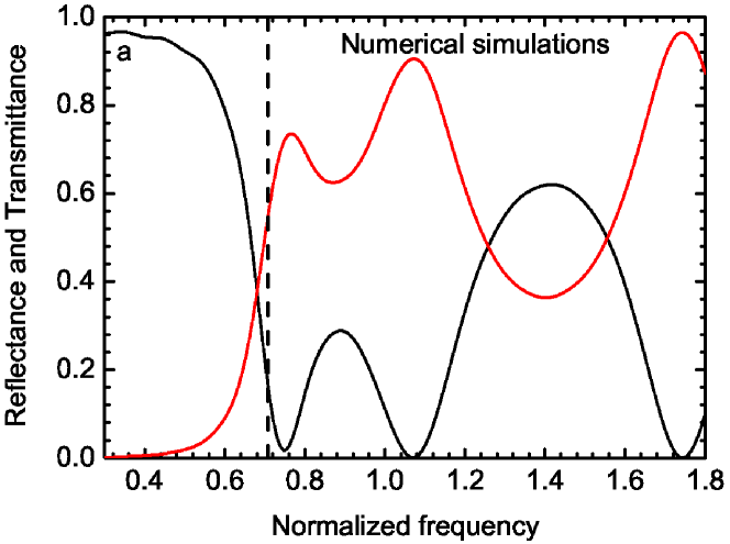
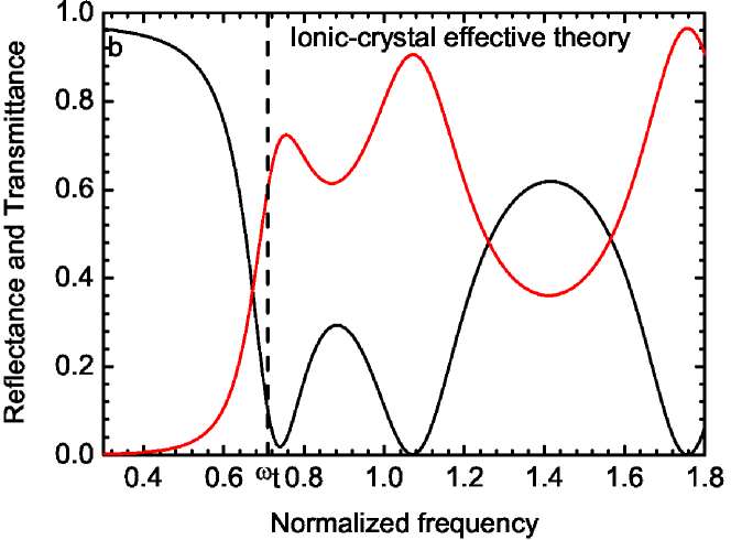
Note finally that the long-wave limit for the second relation (19) reduces to the two solutions and associated with the trivial dispersion laws obtained out of Eq. (IV). Correspondingly, the TE field in that case results to be a constant (along ) and therefore simply vanishes due to the symmetry condition .
VI Comments and Conclusion
When the long-wave limit is not accurate enough, one might think of solving numerically the dispersion relations (10) and (11) to calculate . However, beyond the long-wave approximation, the main effect to take into account is the occurrence of guided modes, primarily inside the undoped semiconductor. In that case one must reconsider the problem since the method of the effective layer would simply fail.
The presence of two types of modes makes it uneasy to define in general the stop band which is not always . By looking at the dispersion relations, close to the long-wave limit, we found that the stop band is the interval when , but becomes when . However in that case, the interval is filled with symmetric modes which are not excited under normal incidence, the effective stop band being then still . Note that when , the 2 frequencies and coincide, and the interval is a gap also at oblique incidence.
By comparing realistic numerical simulations with theoretical considerations, we have shown that the nanostructure described in Fig.1 works in TM regime as a single layer with the effective dielectric function (2), representative of SPP generation. This result provides a comprehensive understanding of the system as a whole, on the entire spectrum, to show that it behaves as a ionic-crystal material. Moreover our result provides a powerful tool to explore the possibilities offered by such a metamaterial, e.g. by varying the sizes, the materials and the doping level, with the opportunity to reach the visible range.
Note finally that, in view of experimental realization, different techniques can be adopted as e.g., epitaxy, deposition, etching or implantation. Although these are well proved techniques, the resulting optical properties of the structure will be affected by imperfections such as interface roughness, diffusion, geometrical defects, which requires further studies.
References
- (1) H. Raether, Surface Plasmons, Springer Tracts in Modern Physics Vol. 111 (Springer, Berlin, 1988).
- (2) A.V. Zayatsa, I.I. Smolyaninovb, A.A. Maradudinc, Phys. Rep. 408 (2005) 131.
- (3) S.A. Maier, Plasmonics, fundamentals and applications, Springer (2007) New-York
- (4) K.Y. Bliokh, Y.P. Bliokh, V. Freilikher, S. Sevel’ev, F. Nori, Rev. Mod. Phys. 80 (2008) 1201.
- (5) D.K. Gramotnev, S.I. Bozhevolnyi, Nature Photonics 4 (2010) 83.
- (6) S. C. Kitson, W. L. Barnes, and J. R. Sambles, Phys. Rev. Lett. 77 (1996) 2670.
- (7) S.I. Bozhevolnyi, J. Erland, K. Leosson, P.M.W. Skovgaard, J.M. Hvam, Phys. Rev. Lett. 86 (2001) 3008.
- (8) T. W. Ebbesen, H. J. Lezec, H. F. Ghaemi, T. Thio, and P.A. Wolff, Nature 391 (1998) 667.
- (9) S. Collin, G. Vincent, R. Haïdar, N. Bardou, S. Rommeluère, J-L. Pelouard, Phys. Rev. Lett., 104 (2010) 027401.
- (10) V.V. Temnov, G. Armelles, U. Woggon, D. Guzatov, A. Cebollada, A. Garcia-Martin, J-M. Garcia-Martin, T. Thomay, A. Leitenstorfer, R. Bratschitsch, Nature Photonics 4 (2010) 107.
- (11) Ye Pu, R. Grange, Chia-Lung Hsieh, D. Psaltis, Phys. Rev. Lett. 104 (2010) 207402.
- (12) Seungchul Kim, Jonghan Jin, Young-Jin Kim, In-Yong Park, Yunseok Kim, Seung-Woo Kim, Nature 453 (2008) 757.
- (13) R.D. Kekatpure, E.S. Barnard, W. Cai, M.L. Brongersma, Phys. Rev. Lett. 104 (2010) 243902.
- (14) T. Utikal, M.I. Stockman, A.P. Heberle, M. Lippitz, H. Giessen, Phys. Rev. Lett. 104 (2010) 113903.
- (15) Cheng-ping Huang, Xiao-gang Yin, Qian-jin Wang, Huang Huang, Yong-yuan Zhu, Phys. Rev. Lett. 104 (2010) 016402.
- (16) E. N. Economou, Phys. Rev. 182 (1969) 539.
- (17) J.A. Porto, L. Martin-Moreno, F.J. Garcia-Vidal, Phys Rev B 70 (2004) 081402(R).
- (18) G.A. Wurtz, R. Pollard, A.V. Zayats, Phys Rev Lett 97 (2006) 057402
- (19) Y.B. Li, R.A. Stradling, T. Knight, J.R. Birch, R.H. Thomas, C.C. Philips, I.T. Ferguson, Semicond. Sci. Technol. 8 (1993) 101
- (20) FDTD solutions 6.5, Lumiercial Solution Inc., (Canada).
- (21) M. Born, E. Wolf, Principles of Optics, Cambridge Univ. Press, Cambridge, UK, (1999).