Disorder induced Coulomb gaps in graphene constrictions with different aspect ratios
Abstract
We present electron transport measurements on lithographically defined and etched graphene nano-constrictions with different aspect ratios, including different length () and width (). A roughly length-independent disorder induced effective energy gap can be observed around the charge neutrality point. This energy gap scales inversely with the width even in regimes where the length of the constriction is smaller than its width (). In very short constrictions we observe both resonances due to localized states or charged islands and an elevated overall conductance level (0.1 - 1), which is strongly length-dependent in the gap region. This makes very short graphene constrictions interesting for highly transparent graphene tunneling barriers.
pacs:
71.10.Pm, 73.21.-b, 81.05.Uw, 81.07.TaGraphene nanoribbons and constrictions che07 ; han07 ; dai08 ; wan08 ; mol09 ; sta09 ; tod09 ; liu09 ; mol10 ; gal10 ; han10 are promising candidates to overcome the gapless nature of graphene gei07 . Graphene, a truly two-dimensional (2D) semi-metal with unique electronic properties, is becoming increasingly interesting for high mobility ultra-fast nanoelectronics kat07 . However, the missing band gap in graphene makes it difficult to realize graphene switches, transistors, and logic devices in general. By tailoring graphene into narrow ribbons or constrictions, the formation of an energy gap has been shown.
Graphene constrictions have been successfully demonstrated to act as tunneling barriers in single electron transistors sta08b , quantum dots pon08 ; gue09 and more recently in double quantum dots mol09a ; mor09 ; liu10 . The nature of the observed energy gaps has been discussed in great detail. From the theoretical point of view, different models have been put forward to describe the observed energy gap including quasi-1D Anderson localization eva08 ; que08 ; gun08 ; lhe08 ; muc09 ; mar09 , percolation ada08 or Coulomb blockade on a series of localized states sol07 . Experimentally, the nanoribbon width-dependence of the energy gap has been studied by a number of groups and it has been found that the gap size is mainly given by the charging energy of small isolated islands forming in the nanoribbon due to disorder sta09 ; tod09 . However, only recently has the influence of the nanoribbon length, , been investigated systematically for nanoribbons with width nm gal10 ; han10 . So far, the experimentally studied graphene nanostructures exhibited an aspect ratio of , such that the width was the smallest and dominating length scale.
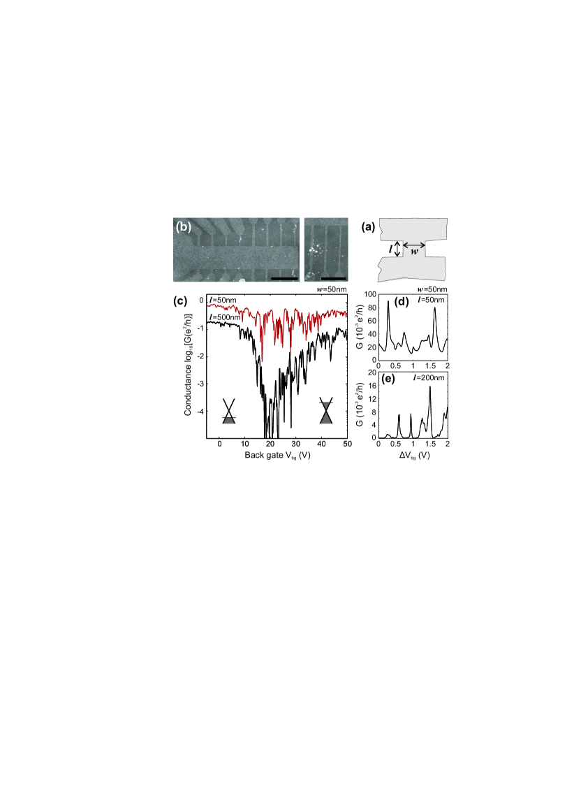
Here, we present a systematic study of electronic transport in graphene constrictions with different aspect ratios, including both different width and length. In particular, we focus on graphene constrictions in the regime of and [see Fig. 1(a)]. We show that in these regimes, the Coulomb charging energy of the smallest disorder-induced charged island in the constriction sta09 ; tod09 is still predominantly determined by the width. However, the overall conductance level is strongly influenced by the length of the constriction. Most interestingly, we show that in very short constrictions, Coulomb blockade diamonds with high transparency can be observed.
The samples have been fabricated from graphene that has been mechanically exfoliated from natural bulk graphite and deposited onto 295 nm SiO2 on a highly p-doped Si substrate. Raman spectroscopy is used to verify the single-layer character of the investigated graphene nanostructures dav07a . Electron-beam (e-beam) lithography is used to pattern the etch mask ( 110 nm of e-beam resist) for structuring the graphene devices.

Reactive ion etching based on an Ar/O2 plasma is employed to remove unprotected graphene. Scanning force microscope images of etched graphene nanostructures after removing the residual resist are shown in Fig. 1(b). Finally, the graphene devices are contacted by e-beam patterned 5 nm Cr and 50 nm Au electrodes.

The measurements have been performed in a pumped 4He system at 1.3 K. We have measured the current through the two-terminal constrictions by applying a small symmetric DC bias voltage . The differential conductance has been measured directly by low-frequency lock-in techniques by adding an AC bias of 100 V.
In Fig. 1(c) we show the conductance as function of back gate (BG) voltage for two 50 nm wide constrictions with different length nm and nm ( = 500 V). The transport gap, i.e. the region of suppressed conductance (roughly between 17 and 30 V), separates hole from electron transport as indicated by the two lower inserts in Fig. 1(c) com01 . Whereas for the nm constriction the conductance is strongly suppressed in this regime (down to ), we observe a significantly increased conductance for the shorter constriction. Nevertheless, a number of pronounced resonances reaching lower conductance values mark the gap region in rather good agreement with the measurement on the longer constriction [compare also Fig. 2(a) and 2(b)]. A close-up of such resonances is shown in Fig. 1(d). These reproducible resonances have been taken at V within the BG range of minimum conductance. We observe neither complete pinch-off nor strong Coulomb blockade behavior, as is found for longer constrictions with the same width. For example, in Fig. 1(e) we show data recorded on a nm long ( nm) constriction. The overall conductance level differs significantly, however the typical spacing between the resonances is comparable.

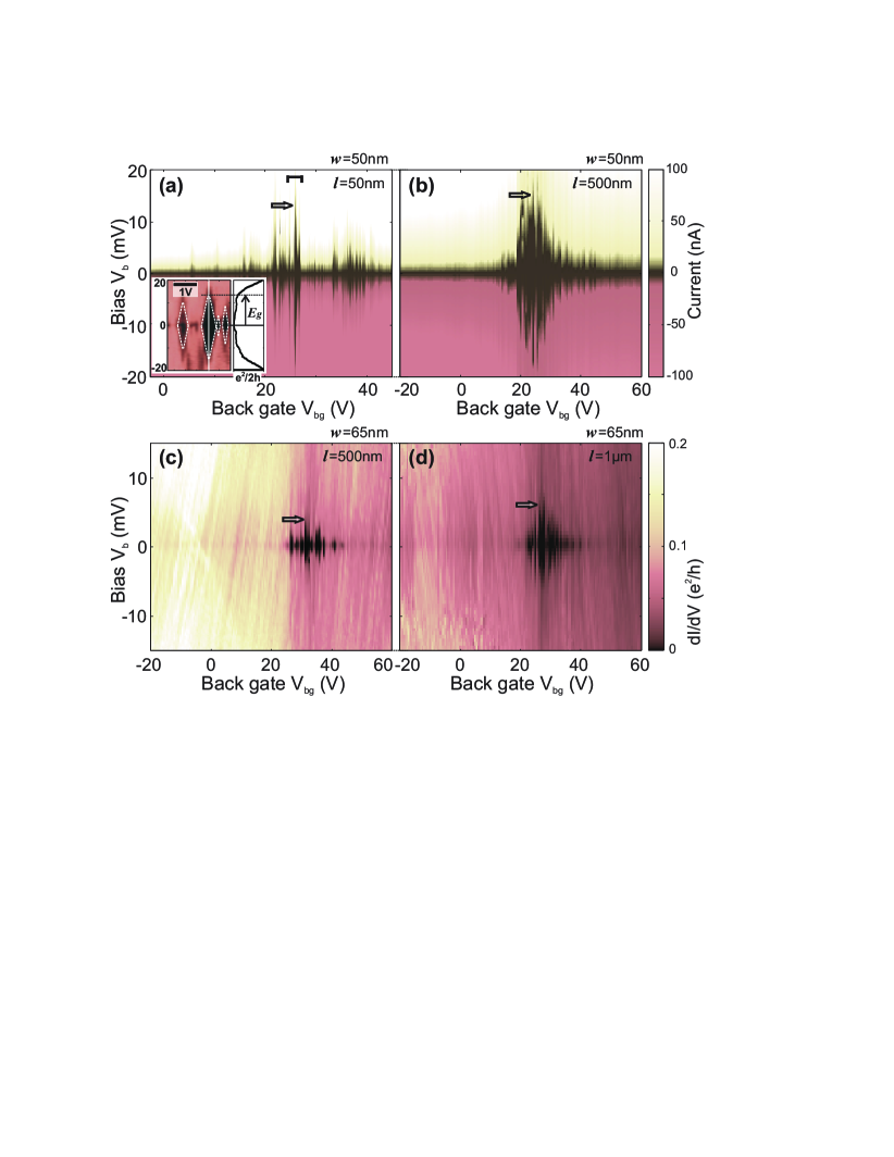
In Figs. 2(a), 2(b) we show 2D-plots of current as function of bias and back gate voltage for the two nm wide constrictions with nm (a) and nm (b). In good agreement with earlier studies han07 ; mol09 ; sta09 ; tod09 ; liu09 ; mol10 ; gal10 ; han10 we find regions of suppressed current with an extension of in the direction (see arrows). By plotting higher-resolution measurements of the differential conductance, one can see that the region of suppressed current is composed of individual diamonds [see inset in Fig. 2(a)]. The energy gap corresponds to the charging energy of the largest diamond sta09 ; tod09 , as highlighted in the inset [see arrow in Fig. 2(a)]. Interestingly, this energy scale only weakly depends on the constrictions length. By comparing Figs. 2(a) and 2(b) we observe only a small difference in between the nm ( = 13 meV) and nm ( = 15 meV) long constriction, allowing the conclusion that the smallest island or localized state is predominantly a function of the width, . The main difference can be found in the back gate coverage of the observed gaps. The shorter the constriction, the fewer islands [or localized (edge) states] are in the constriction, leading to fewer charging events. Consequently, the current is suppressed in smaller and fewer gate voltage regimes. However, the smallest island is found to be roughly length-independent (this is also true for ). The definition of the transport gap in BG voltage mol09 ; mol10 , used as figure of merit in earlier work, is hard to define for very short constrictions since it is considered to strongly depend on the disorder potential sta09 ; tod09 ; gal10 , which becomes very sample dependent, due to lack of averaging.
Similar behavior can also be seen for a nm wide, nm and m long constriction, as shown in Figs. 2(c) and 2(d), respectively. Here we plot the differential conductance as a function of and . In both measurements, a maximum charging energy of around 4.5 and 6 meV can be observed (see arrows).

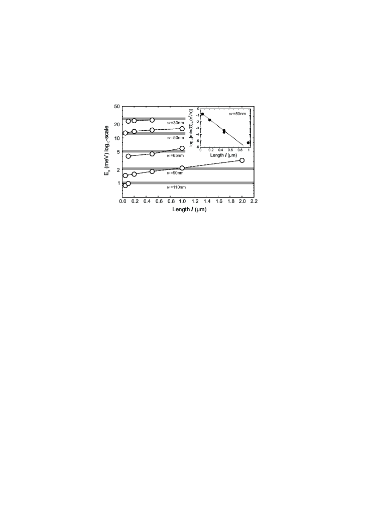
In total, we studied roughly 20 graphene constrictions on 3 different samples. In Fig. 3 we summarize the extracted energy gaps as a function of the length for 5 different widths com02 . It can be seen that strongly depends on the width and we find good agreement with earlier experiments and theoretical models sol07 ; han10 . In particular, we compare our results with the model from Sols et al., sol07 where the energy gap is approximated by , (see gray bars in Fig. 3), see also han07 ; sol07 ; mol10 . In contrast to the weak -length dependence, we observe a rather strong length dependence of the minimum conductivity, as shown by the inset in Fig. 3. The minimum value of the running averaged conductance decreases exponentially with increasing constriction length. This fits well with the scenario where localizations or tunneling processes are dominating the transport through the constrictions. Moreover, it shows that by making graphene constrictions very short, we can obtain conductance level close to .
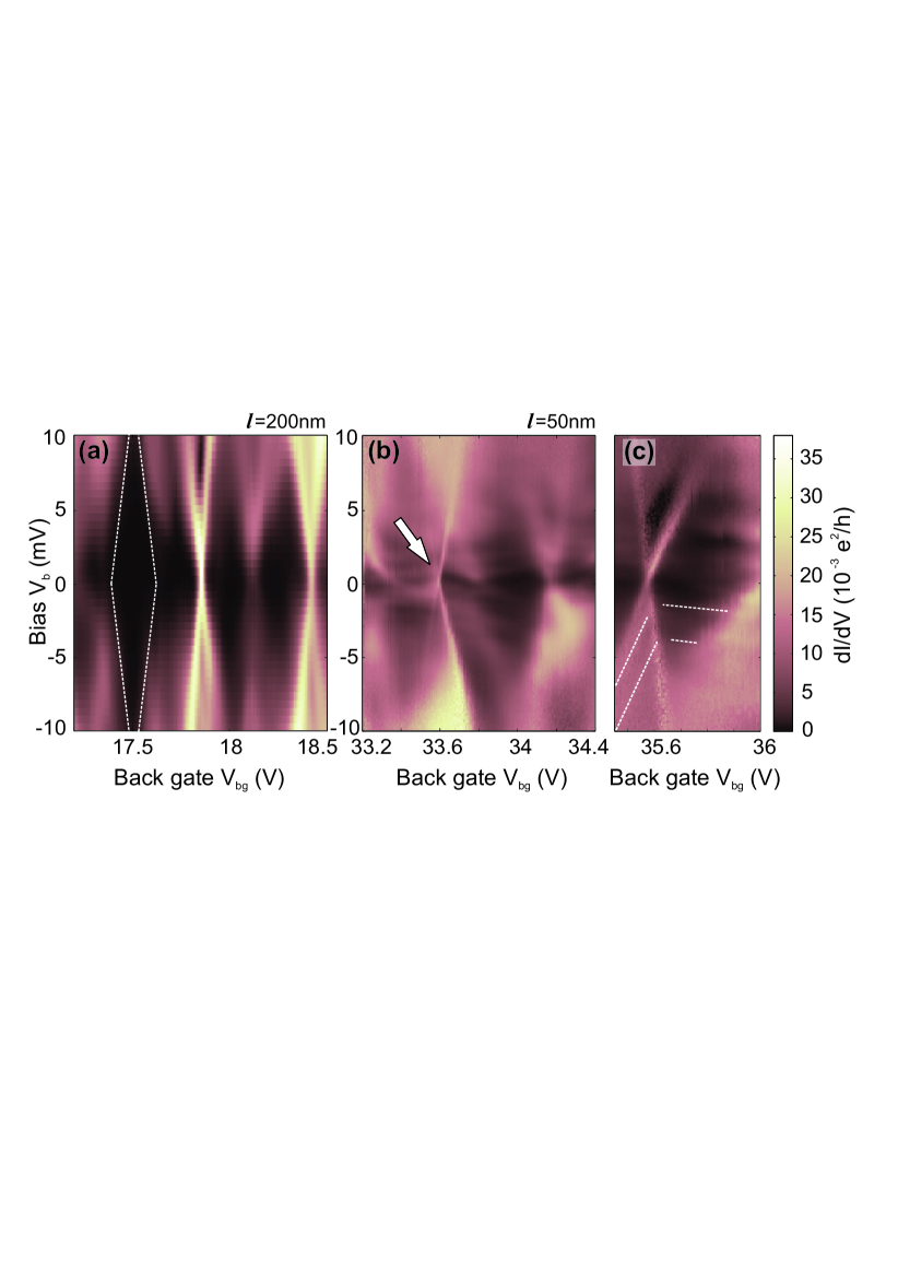
More insights on the transparency of the shorter constrictions is gained by focusing on a small BG voltage range as shown in Fig. 4. Here, we show high-resolution differential conductance plots for different constriction lengths with constant width (=50 nm). Measurements on a 200 nm long constriction [Fig. 4(a)] show well-distinguishable diamonds of suppressed conductance in good agreement with earlier studies. In shorter constrictions [=50 nm; Figs. 4(b),4(c)] we observe diamonds where the conductance is not fully suppressed, most likely because of strong coupling to localized states or isolated charged islands. Moreover, we observe faint lines of increased conductance inside diamonds aligned with features outside the diamonds, which might be due to inelastic co-tunneling [see e.g. dashed lines in Fig. 4(c)]. According to recent experiments by Han et al. han10 the average hopping length is in the range of . Consequently, it is likely that for very short constrictions exceeds (), so that transport in short constrictions is no longer effectively 1D, resulting in several transport channels in the constrictions. This would account for (i) the strong increase in conductance and (ii) the appearance of very sharp features in the conductance [see e.g. arrow in Fig. 4(b)], which could result from interference effects or Fano resonances.
In summary, we presented transport measurements on graphene nano-constrictions with different aspect ratios. We showed that the strongly width-dependent disorder induced energy gap is roughly length-independent, whereas the overall conductance level depends strongly on the length. In the gap region of very short graphene constrictions, a conductance level close to 0.1e2/h can be reached, making these structures potential candidates for exploring Fano resonances and Kondo physics in graphene nanostructures.
Acknowledgment — The authors wish to thank C. Barengo, P. Studerus, M. Morgenstern, D. Grützmacher, P. Kordt, J. Schirra and S. Gustavsson for their support and help in setting up our new lab. We thank A. Steffen, R. Lehmann and J. Mohr for the help on the sample fabrication. Discussions with H. Lüth, T. Heinzel, T. Ihn, J. Güttinger and support by the JARA Seed Fund and SPP-1459 are gratefully acknowledged.
References
- (1) Z. Chen, Y.-M. Lin, M. Rooks and P. Avouris, Physica E, 40, 228, (2007).
- (2) M. Y. Han, B. Özyilmaz, Y. Zhang, and P. Kim, Phys. Rev. Lett., 98, 206805 (2007).
- (3) X. Li, X. Wang, L. Zhang, S. Lee, H. Dai, Science, 319, 1229 (2008).
- (4) X. Wang, et al., Phys. Rev. Lett., 100, 206803 (2008).
- (5) F. Molitor, et al., Phys. Rev. B, 79, 075426 (2009).
- (6) C. Stampfer, et al., Phys. Rev. Lett., 102, 056403 (2009).
- (7) K. Todd, et al., Nano Lett., 9, 416 (2009).
- (8) X. L. Liu, et al., Phys. Rev. B, 80, 121407 (2009).
- (9) F. Molitor, et al., Semicond. Sci. Technol., 25, 034002 (2010).
- (10) P. Gallagher, et al., Phys. Rev. B, 81, 115409 (2010).
- (11) M. Y. Han, et al., Phys. Rev. Lett., 104, 056801 (2010).
- (12) A. K. Geim and K. S. Novoselov, Nat. Mater., 6, 183 (2007).
- (13) M. I. Katnelson, Materials Today, 10(1-2), 20, 2007.
- (14) C. Stampfer, et al., Nano Lett., 8, 2378 (2008).
- (15) L. A. Ponomarenko, et al., Science, 320, 356 (2008).
- (16) J. Güttinger, et al., Phys. Rev. Lett., 103, 046810 (2009).
- (17) J. Moser and A. Bachtold, Appl. Phys. Lett., 95, 173506 (2010).
- (18) F. Molitor, et al., Appl. Phys. Lett., 94, 222107 (2009).
- (19) S. Moriyama, et al., Nano Lett., 9, 2891 (2009).
- (20) X. L. Liu, et al., Nano Lett., 10, 1623 (2010).
- (21) M. Evaldsson et al., Phys. Rev. B, 78, 161407(R) (2008).
- (22) D. Querlioz et al., Appl. Phys. Lett., 92, 042108 (2008).
- (23) D. Gunlycke, et al., Appl. Phys. Lett., 90, 142104 (2007).
- (24) A. Lherbier et al., Phys. Rev. Lett., 100, 036803 (2008).
- (25) E. R. Mucciolo, et al., Phys. Rev. B, 79, 075407 (2009).
- (26) I. Martin and Y. M. Blanter, Phys. Rev. B, 79, 235132 (2009).
- (27) S. Adam, et al., Phys. Rev. Lett., 101, 046404 (2008).
- (28) F. Sols, et al., Phys. Rev. Lett., 99, 166803 (2007).
- (29) D. Graf, et al., Nano Lett. 7, 238 (2007).
- (30) All samples are slightly p-doped most likely due to residual resist on the graphene structures.
- (31) Since the extracted gap is strongly disorder dependent the error bars are around 5-10%, in agreement with earlier studies. For clarity error bars are not shown explicitly in Fig. 3.