Present address: ] Center for Nano-Materials and Technology, Japan Advanced Institute of Science and Technology (JAIST), 1-1, Asahidai, Nomi, Ishikawa 923-1292, Japan
Permanent address: ] Electronics Department, Radiophysics Faculty, Nizhny Novgorod State University, Nizhny Novgorod 603950, Russia
Spin-orbit coupling and phase-coherence in InAs nanowires
Abstract
We investigated the magnetotransport of InAs nanowires grown by selective area metal-organic vapor phase epitaxy. In the temperature range between 0.5 and 30 K reproducible fluctuations in the conductance upon variation of the magnetic field or the back-gate voltage are observed, which are attributed to electron interference effects in small disordered conductors. From the correlation field of the magnetoconductance fluctuations the phase-coherence length is determined. At the lowest temperatures is found to be at least 300 nm, while for temperatures exceeding 2 K a monotonous decrease of with temperature is observed. A direct observation of the weak antilocalization effect indicating the presence of spin-orbit coupling is masked by the strong magnetoconductance fluctuations. However, by averaging the magnetoconductance over a range of gate voltages a clear peak in the magnetoconductance due to the weak antilocalization effect was resolved. By comparison of the experimental data to simulations based on a recursive two-dimensional Green’s function approach a spin-orbit scattering length of approximately 70 nm was extracted, indicating the presence of strong spin-orbit coupling.
I Introduction
Semiconductor nanowires fabricated by a bottom-up approachThelander et al. (2006); Lu and Lieber (2006); Ikejiri et al. (2007) offer an exciting route to study fundamental quantum effects in electron transport of nanostructures.Franceschi et al. (2003); Fasth et al. (2005); Pfund et al. (2006); van Dam et al. (2006); Fuhrer et al. (2007); Richter et al. (2008) By choosing a narrow-band gap semiconductor for the nanowire, i.e. InAs or InN, the common problem connected with carrier depletion at the surface can be avoided.Thelander et al. (2006); Chang et al. (2005); Calarco and Marso (2007); Blömers et al. (2008a); Ford et al. (2009) As illustrated in Fig. 1(a), for these semiconductors a surface accumulation due to the Fermi-level pinning in the conduction band occurs.Lueth (2010) Here, due to the electron transfer from the surface states the conduction and valence bands are bent downwards and a two-dimensional electron gas (2DEG) is formed at the surface. The electrons are confined in a triangularly-shaped potential well. In the case of InAs-based semiconductors it is known that the electrons in the accumulation layer are also subject to the impact of a strong spin-orbit coupling.Nitta et al. (1997); Engels et al. (1997); Schierholz et al. (2004) The macroscopic electric field in the triangularly-shaped quantum well lifts the spin-degeneracy for propagating electrons. This so-called Rashba effectBychkov and Rashba (1984) is of relevance for spin electronic devices, since it can be employed for gate-controlled spin manipulation.Datta and Das (1990) It was shown theoretically that by making use of quantum wire structures the performance of spin transistor structures with respect output modulation can be improved and devices with new functionalities, e.g. spin filters, can be realized.Datta and Das (1990); Bournel et al. (1998); Governale et al. (2002); Zülicke and Governale (2002) Experimentally the presence of spin-orbit coupling can be verified by the observance of the weak antilocalization effect.Bergmann (1984); Hikami et al. (1980) For one-dimensional structures the spin-orbit scattering length being a measure of the strength of spin-orbit coupling can be determined by fitting an appropriate theoretical model.Kurdak et al. (1992); Kettemann (2007); Wenk and Kettemann (2010)
At low temperatures the electron transport in a nanowire is governed by electron interference. The relevant parameter connected to this phenomenon is the phase-coherence length . If the length of the nanowire is comparable to one finds conductance fluctuates with an amplitude on the order of if a magnetic field is applied or if the electron concentration is changed by means of a gate electrode.Hansen et al. (2005); Blömers et al. (2008a, b) The fluctuations originate from the fact that in small disordered samples, electron interference effects are not averaged out.Al’tshuler (1985); Lee et al. (1987) Although fluctuations in the conductance can mask other quantum effects, i.e. weak localization or quantized conductance, important information on the electron transport can be gained from the statistical properties of the fluctuations themselves.
We studied the transport properties of small individual InAs nanowires and demonstrate that in spite of the fact that the low-temperature magneto-conductance strongly fluctuates the essential transport parameters, e.g. or the spin-orbit scattering length can be extracted. Information on at various temperatures is obtained from the average fluctuation amplitude as well as from the correlation field. As mentioned above, for electrons confined at the surface a strong Rashba spin-orbit coupling is expected, due to the high electric field in the quantum well.Engels et al. (1997) Previously, for individual InAs wiresDhara et al. (2009); Roulleau et al. (2010) or InAs wires contacted in parallelHansen et al. (2005) a maximum of the magnetoconductance at zero field due to weak antilocalization was reported indicating the presence of spin-orbit coupling, whereas no weak antilocalization in InAs nanowires was found by others.Liang et al. (2009)
It is known for InAs nanowires that depending on the growth conditions different crystal structures form, which have a direct impact on the transport properties.Schroer et al. (2009) Our nanowires were grown by using selective-area metal-organic vapor phase epitaxy. In this case no metallic particles were used in contrast to the vapor-liquid-solid growth which is mostly employed for InAs nanowire growth.Thelander et al. (2006) Since our method is different we were interested if indications spin-orbit coupling can be observed as well. However, the growth method we used limits maximum nanowire length to a few micrometers.Akabori et al. (2009) The short nanowire length is the reason that strong conductance fluctuations occur in our magnetotransport experiments masking the weak antilocalization effect. Nonetheless, by making use of averaging the conductance with respect to the gate voltage,Petersen et al. (2009) we were able to resolve weak antilocalization. Thus by the method applied here one can assess the strength of spin-orbit coupling even in the presence of conductance fluctuations. The measured characteristics of the weak antilocalization is compared to calculated characteristics based on a recursive real-space Green’s function approach. In contrast to previous theoretical models treating quantum wires based on a planar 2DEG, here the cylindrical symmetry of the surface 2DEG is taken explicitly into account.
II Experimental
The InAs nanowires were selectively grown on a patterned GaAs (111)B substrate by low-pressure metal-organic vapor phase epitaxy in an N2 atmosphere at a temperature of 650∘C.Akabori et al. (2009) The wires have a diameter of approximately 100 nm. Figure 1(b) shows a scanning electron micrograph of the as-grown InAs nanowires.
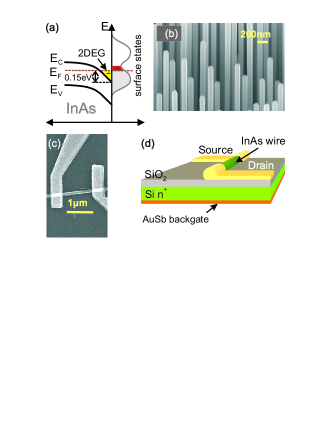
For the transport measurements contact pads and adjustment markers were defined on an -type doped Si (100) wafer covered by a 100-nm-thick SiO2 layer. The SiO2 layer was prepared by thermal oxidation. The InAs nanowires were dispersed on the patterned substrate, by separating them first from their host substrate in an acetone solution. Subsequently, a droplet of acetone containing the detached InAs nanowires was put on the patterned substrate. The nanowires were contacted individually by a pair of Ti/Au electrodes using electron beam lithography. In order to improve the contact resistance Ar+ sputtering was employed prior to the metal deposition. The substrate was used as a back-gate to control the electron concentration. The contact separation of the wire reported here was 1 m. In Fig. 1(c), an electron beam micrograph of the sample is shown, while in Fig. 1(d) a schematics of the sample layout can be found. In total three nanowires were measured which showed similar properties as the one presented here. At zero gate voltage the nanowire has a resistance of 30.0 k after subtracting the typical contact resistance of 1 k. The contact resistance and resistivity was estimated by resistance measurements at 4 K of many nanowires of the same growth run with different contact separations. The typical electron concentration of cm-3 was determined by extracting the threshold voltage from the low-temperature transfer characteristics on more than ten samples using the method described in Ref. [Dayeh et al., 2007]. For the mobility we obtained a low-temperature value of 3300 cm2/Vs. The value of the diffusion constant , with the Fermi velocity determined from and the elastic scattering time calculated from , is equal to cm2/s. The Fermi energy is estimated to be about 60 meV.
The magneto-transport measurements were performed in a He-3 cryostat at temperatures ranging from 0.5 K to 30 K. The magnetoresistance was measured by using a lock-in technique with an ac bias current of 5 nA and a magnetic field oriented perpendicular to the wire axis.
III Simulation
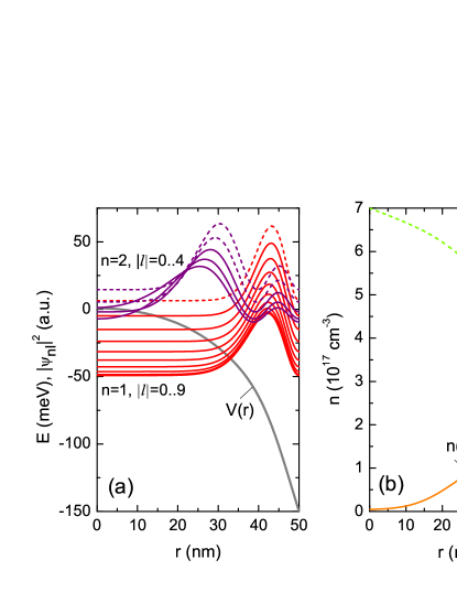
In order to illustrate the interface accumulation layer of an InAs nanowire with Fermi level pinning within the conduction band, we calculated the quantum states in a nominally undoped InAs nanowire at . The calculations were performed by employing a Schrödinger–Poisson solver dedicated to cylindrically shaped conductors. The contribution of disorder, i.e. due to impurities or interface roughness was not taken into account. For the surface Fermi level pinning a value of 0.15 eV was assumed, which is a common value for InAs.Smit et al. (1989); Lueth (2010) At the interface an infinite potential barrier was taken. In order to account for the conduction band non-parabolicity, we inserted an enhanced effective mass of . Instead of employing an energy-dependent effective mass, we used a simpler approach proposed by Schierholz et al.,Schierholz et al. (2004) where the average effective mass is a function of the electron concentration. Using these parameters the calculated integrated electron density agreed well with the experimental average concentration of cm-3. The calculated conduction band profile is shown in Fig. 2(a) together with the probability density for the first () and second () subbands at different angular momenta . Due to the Fermi level pinning at the surface, a potential well with an approximately triangular shape is formed. This is also reflected by the electron density shown in Fig. 2(b), where a surface accumulation layer is formed with a maximum value of being 8 nm below the surface. As can also be seen in Fig. 2(b), the absolute value of the electric field increases monotonously for increasing radius, reaching a value of about V/cm where reaches its maximum.
IV Experimental Results and Discussion
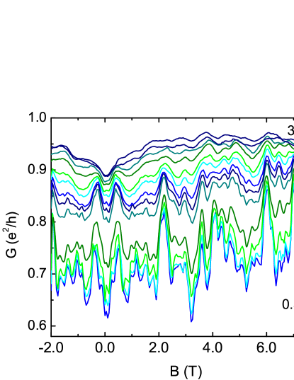
We will first focus on the transport properties at zero gate bias, in order to obtain information on the phase-coherence length . In Fig. 3 the magneto-conductance is plotted for various temperatures ranging from 0.5 to 30 K.
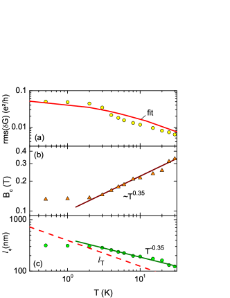
As one can see, on average the conductance increases with temperature. At low temperature the conductance strongly fluctuates, while at higher temperatures these fluctuations are largely smeared out. The average fluctuation amplitude around the mean value of the conductance is quantified by the root-mean-square . Here, the variance is defined by , with the average of the conductance fluctuations over . As can be seen in Fig. 4(a), at temperatures below about 2 K the average amplitude is saturated, while above that temperature decreases monotonously. The corresponding correlation field of the fluctuations is shown in Fig. 4(b). The correlation field was extracted from the autocorrelation function of given by , with corresponding to half maximum of the autocorrelation function .Lee et al. (1987) At low temperatures ( K) we find that is approximately constant at 0.13 T, while it increases proportional to for temperatures larger than 2 K. Under the assumption that is larger than the diameter of the nanowire one can extract directly from correlation field using the expressionBeenakker and van Houten (1988)
| (1) |
where is a pre-factor depending on the transport regime. The area corresponds to the maximum area enclosed by phase-coherent time-reversed electron waves penetrated by a single flux quantum . Here, we assumed the dirty metal limit with .Beenakker and van Houten (1988) At temperatures below about 2 K, has its maximum value at about 300 nm, while at higher temperatures decreases proportional to to a value of slightly above 100 nm at K. The cylindrical geometry of our nanowire does not correspond completely to the one-dimensional conductors the above employed theory is based on. Therefore, the parameter and thus might differ. In fact, as one can infer from Fig. 4(b) up to 2 K the correlation field is constant. A possible reason for this might be, that phase-coherent transport is rather limited by the contact separation.Blömers et al. (2008a) Therefore the actual values of are presumably larger than the ones calculated from Eq. (1).
The values of gained from the analysis of were taken to calculate the theoretically expected values for . For this purpose we used the interpolation formula of Beenakker and van Houten given by:Beenakker and van Houten (1988)
| (2) |
Here, is the thermal length. Theoretically, for a value of is expected for the situation that a magnetic field is applied and spin-orbit coupling is present. As can be seen in Fig. 4(a), a satisfactory agreement of the change with temperature between theory and the experimental values of can be obtained, however for a value of 0.34 had to be inserted being a factor of 5 smaller than the theoretically expected value. A possible reason for this discrepancy might also be that in our case the electrons propagate through in a conductor of cylindrical shape, while the theory was developed for a quantum wire based on a two-dimensional electron gas.
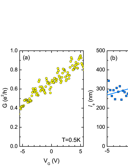
By applying a gate voltage the electron concentration and thus the conductance can be adjusted. As can be seen in Fig. 5(a), by varying from V to V the conductance increases from to almost . On average increases linearly with . The weak dependence of the conductance on the gate voltage can be related to the large thickness of the SiO2 layer and to a large density of interface states. The relatively large variations of can be attributed to conductance fluctuations originating from changes in the electron interference due to the variation of the Fermi wave length.Lee et al. (1987) At fixed gate voltages the conductance fluctuations were recorded as a function magnetic field [cf. Fig. 6(a) and (b)]. One can clearly see, that owing to the two-terminal measurement set-up the fluctuations are symmetric upon reversal of the magnetic field. At different fixed gate voltages the phase-coherence length was determined from of the magneto-conductance fluctuations curves. As can be seen in Fig. 5(b), the resulting values of increase with increasing and thus increasing electron concentration. This increase can be attributed to the decrease of electron-electron scattering rate with increasing Fermi energy.Altshuler and Aronov (1979)
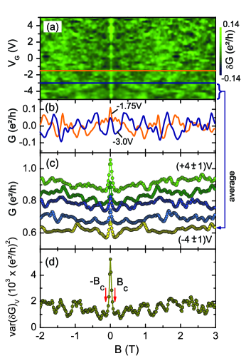
The measurements of the conductance fluctuations as a function of magnetic field were used directly to obtain information on the phase-coherence length , however no phenomena related to spin-effects, i.e. a distinct peak at due to weak antilocalization, are resolved. This is illustrated in Fig. 6(b), where the magnetoconductance fluctuations at a temperature of 0.5 K are plotted for two different back-gate voltages. In both curves no clear peak at zero magnetic field exceeding the average fluctuation amplitude is observed as it is expected for the weak antilocalization effect. In order to resolve weak antilocalization, we made use of averaging uncorrelated fluctuation patterns at different back-gate voltages and thus suppressing the fluctuation amplitude significantly. The underlying data set is shown in Fig. 6(a). The conductance fluctuation patterns are expected to be completely uncorrelated if the change of the Fermi energy induced by the gate voltage exceeds the correlation energy . For the case the correlation energy is given by .Lee et al. (1987) By taking the lower bound value of nm at low temperatures one obtains of about 0.6 meV. Taking to account the value of this corresponds to a gate voltage interval of 0.1 V in which the transport is correlated.
In Fig. 6(c) the magneto-conductance curves from the averaging in successive gate voltage intervals with a width of 2 V are shown. The averaging was performed on magneto-conductance traces for gate voltages each differing by 0.25 V being larger than . A comparison with the single magneto-conductance curves at fixed gate voltages [c.f. Fig. 6(b)] confirms that a considerable damping of the fluctuation amplitude is achieved. Since the gate voltage difference of 0.25 V is larger than estimated above, it is assured that the averaging is performed over statistically independent traces. The choice of the gate voltage interval was a trade-off between an effective averaging to suppress the conductance fluctuations and a sufficiently small change of the phase-coherence length. The chosen width of 2 V meet this requirement. As can clearly be seen in Fig. 6(c), all five traces reveal a clear peak at , which can be attributed to the weak antilocalization effect. When comparing the different gate voltage ranges we find, that for larger gate voltage and thus larger electron concentrations the peak at is higher.
The averaged magneto-conductance curves can be used to estimate the spin-orbit scattering length , being a measure for the strength of spin-orbit coupling. In Fig. 7 the averaged magneto-conductance correction is plotted for the five different gate voltage intervals together with the results of numerical simulations based on a recursive two-dimensional real-space Green’s function approach,Th. Schäpers et al. (2006) where the Rashba spin-orbit coupling is modelled via an effective Hamiltonian . Here, is the Rashba coupling parameter, being a measure of the strength of spin-orbit coupling and associated to the spin-orbit length , are the Pauli spin matrices, and is the electron wave vector. In order to take into account the cylindrical geometry of the wires, periodic boundary conditions are imposed to mimic a plane wave propagation along the transverse direction, as well as a sinusoidal external magnetic field. In our zero-temperature calculations we assume the presence of purely elastic scattering and the wire length plays the role of dephasing length .Th. Schäpers et al. (2006) The numerical scheme consists in dividing the system into one-dimensional slices along the transport direction and to compute the isolated Green’s functions of each slice. Hence, the total Green’s function is obtained by recursively connecting the on-site Green’s function via a procedure based on the Dyson equation. Ohmic contacts are included by means of self-energies obtained from the surface Green’s function of semi-infinite leads. We assume that the external leads attached to our system are subject to the same homogeneous magnetic field as is present in the sample, but have no spin-orbit coupling. Magnetic field in the channel is accounted for by multiplying Peierls phases to the hopping elements of the Hamiltonian.Baranger91 The conductance is expressed by the Landauer-Büttiker formula where the sum runs over all incoming and outgoing channels, and is the transmission probability from mode with spin to mode with spin . Backscattering is induced by an effective potential due to randomly distributed obstacles whose density is tuned, in order to fit the experimental mean free path. Hence, magnetoconductance corrections in Fig. 7 are obtained by averaging hundreds of simulations with different obstacle realizations for an energy range close to the Fermi level.
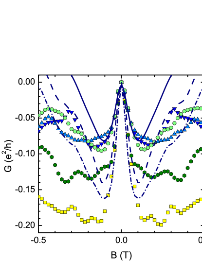
As can be seen in Fig. 7 a satisfactory agreement between the experimentally observed weak-antilocalization peak width and the simulation was achieved for a spin-orbit scattering length of nm. In our simulation we systematically increased from 500 nm, where the resulting peak height fits to the experimental curves at V, V, and 0, to a maximum values of nm. The experimental curve belonging to V fits reasonably well to the simulated curve for nm, while the peak experimental curve for V is even larger that the calculated curve for nm. The steeper decrease of the simulations beyond the conductance minimum is due to the choice of the obstacle potential whose gaussian shape induces a high-field localization stronger than in the real wire. We notice that in our simulations we have compared the experimental data by adopting a phase-coherence length systematically larger than the experimental values plotted in Fig. 4(c). As argued above the values of obtained by employing Eq. (1) might be too small. On the other hand, the discrepancy can also be due to some geometric effect which is not properly described in our model. As can be inferred from the comparison of the experimental data and the simulations Fig. 7, the resulting values of increase with increasing and thus increasing electron concentration. The increase of with increasing electron concentration can be attributed to the decrease of electron-electron scattering rate with increasing Fermi energy.Altshuler and Aronov (1979)
The conclusion that spin-orbit scattering is present in our wires is also supported by the analysis of the variance with respect to the gate voltage taken at different magnetic fields. As can be seen in Fig. 6(d), vs. shows only a single peak at . This is expected from theory for systems comprising a strong spin-orbit coupling.Al’tshuler and Shklovskii (1985); Stone (1989) In this regime the appearance of universal conductance fluctuations is due to the interference of correlated electron pairs in the singlet state only, while the triplet state is suppressed due to spin-orbit coupling. The singlet state can be subdivided in the so-called cooperon and diffusion channels. Applying a magnetic field results in a complete suppression of the magnetic flux sensitive cooperon channel. In fact, the experimentally observed drop of by about a factor of 2.5 is close to the theoretically expected drop by 2. As indicated in Fig. 6(d) the half-width of the peak corresponds to the value of the correlation field T. This feature is in accordance with theory.Al’tshuler and Shklovskii (1985); Stone (1989) Only in the case of systems with weak spin-orbit coupling, a second distinct decrease of the variance originating from the influence of the Zeeman effect at a characteristic field is expected. Here, is the gyromagnetic factor and the Bohr magneton. By assuming for InAs and meV, as has been estimated above, one obtains a value of 0.7 T for . Obviously, by inspecting in Fig. 6(d) one does not find any indication of this second drop. This strongly supports our assumption of the presence of strong spin-orbit coupling in InAs nanowires.
From magnetotransport studies on two-dimensional electron gases formed in the surface accumulation layer of InAs it is well-known that the strong Rashba effect results in a short spin-orbit scattering length . By investigating the characteristic beating pattern in the Shubnikov–de Haas measurementsMatsuyama et al. (2000) or by measuring the weak antilocalization effect Schierholz et al. (2004) values of in the order of 100 nm were found being also confirmed by theoretical calculations.Lamari (2001) In InAs nanowires weak antilocalization was also observed by Hansen et al.,Hansen et al. (2005), here the suppression of conductance fluctuations was achieved by measuring many nanowires in parallel. Typical values of in the order of 200 nm were extracted. On longer InAs nanowires where the conductance fluctuations are sufficiently suppressed values between 200 and 100 nm depending on the electron concentration were obtained by Dhara et al.Dhara et al. (2009) Very recently, on gated InAs nanowires values between 50 nm and 150 nm depending on the nanowire diameters were reported by Roulleau et al.Roulleau et al. (2010) Thus our data obtained for short InAs nanowires showing strong magneto-conductance fluctuations are in good agreement with the experimental values previously reported for other types of InAs nanowire systems. This demonstrates the reliability of our approach.
For a planar surface two-dimensional electron gas in InAs the Rashba parameter was evaluated theoretically by Lamari. Lamari (2003) For an electron concentration comparable to our eVm was calculated. Following the approach of Lamari we assessed based on the electric field averaged over all occupied states : .Th. Schäpers et al. (1998) The calculated electric field is shown in Fig. 2(b). The Rashba coupling parameter was estimated by using the following expression:Engels et al. (1997)
| (3) |
with the interaction parameter for InAs, while and are the band gap and the valence band spin-orbit splitting, respectively.Landolt-Börnstein (2002) Using Eq. (3) we obtained eVm, resulting in a spin-orbit scattering length of 170 nm. The fact that the value for obtained in our calculation is smaller than the ones experimentally obtained by Schierholz et al.Schierholz et al. (2004) and the ones calculated by Lamari Lamari (2003) might be due to the small radius of the wire, since for small radii the Fermi level pinning at the opposite side of the wire leads to an effective softening of the potential profile. In order to check this assumption, we performed a simulation for InAs wires with a sufficiently large diameter so that the shape of the interface potential approaches the one for a planar InAs surface. Here, we found that the values of obtained by LamariLamari (2003) are reproduced. However, one should realize that the assumption of an infinitive interface barrier is oversimplified.Winkler (2003) In fact, for a more rigorous treatment the details of the surface potential profile has to be included. Anyhow, since the surface of the InAs is directly exposed to the environment, no reliable assumption can be made at this stage. This is probably the reason for the larger value of nm resulting from obtained from Eq. (3), compared to the value of 70 nm extracted from the comparison of the experimental weak-antilocalization curves with the simulations based on the Green’s function approach.
V Conclusions
In summary, we determined the relevant low-temperature transport parameters of short InAs nanowires by analyzing the fluctuating magnetoconductance in detail. At the lowest temperature of 0.5 K a phase-coherence length of at least 300 nm was extracted from the correlation field . Above 2 K a decrease of proportional to was observed, which is in accordance with theoretical predictions. Information on the spin-orbit scattering length was gained by averaging the magnetoconductance fluctuations over different gate voltages and comparing these results to simulations based on a recursive Green’s function approach. We find that is in the order of 70 nm indicating the presence of strong spin-orbit coupling. Our investigations thus clearly prove the presence of spin-orbit coupling in short InAs nanowires, which is an important prerequisite for the realization of future spin electronic devices based on semiconductor nanowires.
We gratefully acknowledge M. Governale (Victoria University of Wellington, New Zealand) and A. Bringer (Institute of Solid State Research, Forschungszentrum Jülich) for fruitful discussions. This work was financial support by the French ANR (Quantamonde project) and by DFG through FOR 912.
References
- Thelander et al. (2006) C. Thelander, P. Agarwal, S. Brongersma, J. Eymery, L. Feiner, A. Forchel, M. Scheffler, W. Riess, B. Ohlsson, U. Gösele, and L. Samuelson, Materials Today 9, 28 (2006).
- Lu and Lieber (2006) W. Lu and C. M. Lieber, J. Phys. D: Appl. Phys. 39, R387 (2006).
- Ikejiri et al. (2007) K. Ikejiri, J. Noborisaka, S. Hara, J. Motohisa, and T. Fukui, J.Cryst. Growth 298, 616 (2007).
- Franceschi et al. (2003) S. D. Franceschi, J. A. van Dam, E. P. A. M. Bakkers, L. Feiner, L. Gurevich, and L. P. Kouwenhoven, Appl. Phys. Lett. 83, 344 (2003).
- Fasth et al. (2005) C. Fasth, A. Fuhrer, M. T. Bjork, and L. Samuelson, Nano Lett. 5, 1487 (2005).
- Pfund et al. (2006) A. Pfund, I. Shorubalko, R. Leturcq, and K. Ensslin, Appl. Phys. Lett. 89, 252106 (2006).
- van Dam et al. (2006) J. A. van Dam, Y. V. Nazarov, E. P. A. M. Bakkers, S. D. Franceschi, and L. P. Kouwenhoven, Nature 442, 667 (2006).
- Fuhrer et al. (2007) A. Fuhrer, C. Fasth, and L. Samuelson, Appl. Phys. Lett. 91, 052109 (2007).
- Richter et al. (2008) T. Richter, Ch. Blömers, H. Lüth, R. Calarco, M. Indlekofer, M. Marso, and Th. Schäpers, Nano Lett. 8, 2834 (2008).
- Chang et al. (2005) C.-Y. Chang, G.-C. Chi, W.-M. Wang, L.-C. Chen, K.-H. Chen, F. Ren, and S. J. Pearton, Appl. Phys. Lett. 87, 093112 (2005).
- Calarco and Marso (2007) R. Calarco and M. Marso, Appl. Phys. A 87, 499 (2007).
- Blömers et al. (2008a) C. Blömers, Th. Schäpers, T. Richter, R. Calarco, H. Lüth, and M. Marso, Appl. Phys. Lett. 92, 132101 (2008a).
- Ford et al. (2009) A. C. Ford, J. C. Ho, Y.-L. Chueh, Y.-C. Tseng, Z. Fan, J. Guo, J. Bokor, and A. Javey, Nano Lett. 9, 360 (2009).
- Lueth (2010) H. Lüth, Solid Surfaces, Interfaces and Thin Films, 5th edition (Springer–Verlag, Berlin, Heidelberg, New York, 2010).
- Nitta et al. (1997) J. Nitta, T. Akazaki, H. Takayanagi, and T. Enoki, Phys. Rev. Lett. 78, 1335 (1997).
- Engels et al. (1997) G. Engels, J. Lange, Th. Schäpers, and H. Lüth, Phys. Rev. B 55, R1958 (1997).
- Schierholz et al. (2004) C. Schierholz, T. Matsuyama, U. Merkt, and G. Meier, Phys. Rev. B 70, 233311 (2004).
- Bychkov and Rashba (1984) Y. Bychkov and E. I. Rashba, J. Phys. C (Sol. State Phys.) 17, 6039 (1984).
- Datta and Das (1990) S. Datta and B. Das, Appl. Phys. Lett. 56, 665 (1990).
- Bournel et al. (1998) A. Bournel, P. Dollfus, P. Bruno, and P. Hesto, Eur. Phys. J. Appl. Phys. 4, 1 (1998).
- Governale et al. (2002) M. Governale, D. Boese, U. Zülicke, and C. Schroll, Phys. Rev. B 65, 140403/1 (2002).
- Zülicke and Governale (2002) U. Zülicke and M. Governale, Phys. Rev. B 65, 205304/1 (2002).
- Bergmann (1984) G. Bergmann, Phys. Rep. 107, 1 (1984).
- Hikami et al. (1980) S. Hikami, A. I. Larkin, and Y. Nagaoka, Prog. Theor. Phys. 63, 707 (1980).
- Kurdak et al. (1992) C. Kurdak, A. M. Chang, A. Chin, and T. Y. Chang, Phys. Rev. B 46, 6846 (1992).
- Kettemann (2007) S. Kettemann, Phys. Rev. Lett. 98, 176808/1 (2007).
- Wenk and Kettemann (2010) P. Wenk and S. Kettemann, Phys. Rev. B 81, 125309 (2010).
- Hansen et al. (2005) A. E. Hansen, M. T. Björk, C. Fasth, C. Thelander, and L. Samuelson, Phys. Rev. B 71, 205328 (2005).
- Blömers et al. (2008b) C. Blömers, Th. Schäpers, T. Richter, R. Calarco, H. Lüth, and M. Marso, Phys. Rev. B 77, 201301 (2008b).
- Al’tshuler (1985) B. Al’tshuler, Pis’ma Zh. Eksp. Teo. Fiz. [JETP Lett. 41, 648-651 (1985)] 41, 530 (1985).
- Lee et al. (1987) P. A. Lee, A. D. Stone, and H. Fukuyama, Phys. Rev. B 35, 1039 (1987).
- Dhara et al. (2009) S. Dhara, H. S. Solanki, V. Singh, A. Narayanan, P. Chaudhari, M. Gokhale, A. Bhattacharya, and M. M. Deshmukh, Phys. Rev. B 79, 121311 (2009).
- Roulleau et al. (2010) P. Roulleau, T. Choi, S. Riedi, T. Heinzel, I. Shorubalko, T. Ihn, and K. Ensslin, Phys. Rev. B 81, 155449 (2010).
- Liang et al. (2009) D. Liang, M. R. Sakr, and X. P. Gao, Nano Lett. 9, 1709 (2009).
- Schroer et al. (2009) M. D. Schroer and J. R. Petta, Nano Lett. 10, 1618 (2010).
- Akabori et al. (2009) M. Akabori, K. Sladek, H. Hardtdegen, Th. Schäpers, and D. Grützmacher, J. Cryst. Growth 311, 3813 (2009).
- Petersen et al. (2009) G. Petersen, S. Estévez Hernández, R. Calarco, N. Demarina, and Th. Schäpers, Phys. Rev. B 80, 125321 (2009).
- Dayeh et al. (2007) S. Dayeh, D. P. Aplin, X. Zhou, P. K. Yu, E. Yu, and D. Wang, Small 3, 326 (2007).
- Smit et al. (1989) K. Smit, L. Koenders, and W. Mönch, J. Vac. Sci. & Technol. B 7, 888 (1989).
- Beenakker and van Houten (1988) C. W. J. Beenakker and H. van Houten, Phys. Rev. B 37, 6544 (1988).
- Altshuler and Aronov (1979) B. L. Altshuler and A. Aronov, JETP Lett. 30, 482 (1979).
- Th. Schäpers et al. (2006) Th. Schäpers, V. A. Guzenko, M. G. Pala, U. Zülicke, M. Governale, J. Knobbe, and H. Hardtdegen, Phys. Rev. B 74, 081301 (2006).
- (43) H. U. Baranger, D. P. Di Vincenco, R. A. Jalabert, and A. D. Stone, Phys. Rev. B 74, 10637 (1991).
- Al’tshuler and Shklovskii (1985) B. Al’tshuler and B. Shklovskii, Zh. Eksp. Teor. Fiz. [Sov. Phys. JETP 64, 127 (1986)] 91, 220 (1985).
- Stone (1989) A. D. Stone, Phys. Rev. B 39, 10736 (1989).
- Matsuyama et al. (2000) T. Matsuyama, R. Kürsten, C. Meissner, and U. Merkt, Phys. Rev. B 61, 15588 (2000).
- Lamari (2001) S. Lamari, Phys. Rev. B 64, 245340 (2001).
- Lamari (2003) S. Lamari, Phys. Rev. B 67, 165329 (2003).
- Th. Schäpers et al. (1998) Th. Schäpers, G. Engels, J. Lange, Th. Klocke, M. Hollfelder, and H. Lüth, J. Appl. Phys. 83, 4324 (1998).
- Landolt-Börnstein (2002) Landolt-Börnstein, Group III Condensed Matter, vol. III/41 (Springer Verlag, 2002).
- Winkler (2003) R. Winkler, Spin orbit coupling effects in two-dimensional electron and hole systems (Springer–Verlag, Berlin, Heidelberg, New York, 2003).