Quantum Mechanical Simulation of Electronic Transport in Nanostructured Devices by Efficient Self-consistent Pseudopotential Calculation
Abstract
We present a new empirical pseudopotential (EPM) calculation approach to simulate the million atom nanostructured semiconductor devices under potential bias using the periodic boundary conditions. To treat the non-equilibrium condition, instead of directly calculating the scattering states from the source and drain, we calculate the stationary states by the linear combination of bulk band method and then decompose the stationary wave function into source and drain injecting scattering states according to an approximated top of the barrier splitting (TBS) scheme based on physical insight of ballistic and tunneling transport. The decomposed electronic scattering states are then occupied according to the source/drain Fermi-Levels to yield the occupied electron density which is then used to solve the potential, forming a self-consistent loop. The TBS is tested in an one-dimensional effective mass model by comparing with the direct scattering state calculation results. It is also tested in a three-dimensional 22 nm double gate ultra-thin-body field-effect transistor study, by comparing the TBS-EPM result with the non-equilibrium Green’s function tight-binding result. We expected the TBS scheme will work whnever the potential in the barrier region is smoother than the wave function oscillations and if it does not have local minimum, thus there is no multiple scattering as in a resonant tunneling diode, and when a three-dimensional problem can be represented as a quasi-one-dimensional problem, e.g., in a variable separation approximation. Using our approach, a million atom non-equilibrium nanostructure device can be simulated with EPM on a single processor computer.
I Introduction
According to the roadmap of the Semiconductor Industry Association ITRS , MOSFET (metal oxide semiconductor field-effect transistor) channel length will scale down to 22 nm by 2012. In such nanosized devices, quantum mechanical effects play a big role in determining the properties of the system. New quantum mechanical features, like the fact that the electron mean free path is larger than the device dimensions and the single quantum state levels, can be used to enhance device performance and form new functionalities Ieong04 ; Taur02 ; Hiramoto06 . On the other hand, as the size reduces, new obstacles emerge Taur02 ; Iwai04 , such as the short channel effects, source/drain off-state quantum tunnelling current, barrier current leakage and single dopant random fluctuation Roy05 . Over the past 20 years, many methods have been developed to incorporate the quantum mechanical effects into the device simulation Shin07 ; Anantram07 ; Sverdlov08 . The first of that is the inclusion of some quantum mechanical effective potentials in the drift equation based on the gradients of the charge density Iafrate81 ; Ferry93 . Such gradient terms make the charge density smooth near the Si/SiO2 interface, hence incorporating some of the quantum mechanical effects. The so called quantum Poisson drift equation, or quantum hydrodynamic model have been extensively used for device simulations. However, as the device size shrunk further, it was realized that the quantum mechanical wave functions need to be calculated explicitly.
There are many ways to do the Poisson-Schrödinger’s equation depending on the problem to be studied and the computational costs. One way is to calculate the quantum mechanical local density of states, then apply Boltzmann transport equation based on such density of states Jin08 ; Vasileska06 . However, in the ballistic size region, the use of Boltzmann equation itself is questionable. In such cases, the direct solution of the open boundary condition scattering states based on the Schrodinger’s equation is necessary. For example, this has been done for the 1D cases using the nonequilibrium Green’s function approach base on tight-binding model Lake97 . The use of Green’s function also provides a way to incorporate the inelastic scattering processes in the formalism. Recently, three dimensional devices models with hundreds of thousands of atoms have been simulated using the tight-binding model based on the calculation of scattering states Luisier06 ; Luisier09 . But thousands of computer processors are needed for such direct 3D simulations. There are also effective mass calculation for 2D systems using the scattering state approach Lent90 . It involves the solutions of linear equations in the dimension of the number of real space grid points. Overall, the direct simulation for the 3D device model based on quantum mechanical transport equation remains to be nontrivial. Thus, it will be very useful if there is a faster way to do the simulations. One possible approach is to use the stationary eigen states of a closed system (e.g., periodic system) Schrodinger’s equation to represent the quantum mechanical effects of the scattering states Curatola04 ; Trellakis97 ; Abramo00 ; Hanajiri04 ; de Falco05 . The calculation of the eigen states for a closed boundary condition (e.g., periodic boundary condition) problem is much faster than the calculation of an open boundary condition scattering states. This approach is plausible in the sense, at the zero bias potential between the source and drain, the open boundary condition problem is the same as the closed boundary condition problem. Thus, the closed boundary condition solution is a good starting point for the open boundary condition problem. Many of the quantum mechanical effects have already been represented at this close boundary condition level. The challenge however is to find a good approximation to get the charge density from the stationary wave functions when there is a large bias potential, and to find the corresponding electron current. The possibility of such an approximation relies on the fact that the potential profiles for many semiconductor electronic devices are often relatively simple and smooth, when there is no local minimum in the potential, thus no pseudo localized states, the perspective of the coherent multiple scattering is small. Thus, we will exclude ourselves from cases like the resonant tunneling diode (RTD), or complicated molecular electronics. The approximation might be feasible especially in the regime of ballistic transport, here we define it not only as elastic transport (ignoring electron-phonon scattering), but also as a current overcomes a barrier, then flushes through down hill without multiple scattering Jin08 ; Vasileska06 . In the down hill flushing regime, simple approximations like the WGK approximation can be applied. Note that, the scattering states satisfy the same Schrodinger’s equation as the stationary states, albeit their boundary conditions are different. Thus the eigen states might contain the information as needed for a transport problem (e.g., the local density of states). In this work, we will present a new way to obtain the scattering states from the stationary eigen states. As can be seen in the following sections, our approach is physically intuitive, easy to implement, and tested to be accurate for the smooth barrier potential cases as described above.
Besides the open boundary condition and close boundary condition problem, there is an issue of what Hamiltonian to be used to describe the electronic property of the system. We will use empirical pseudopotential method (EPM) as our Hamiltonian to study the problem. We have mentioned the tight-binding model Lake97 ; Luisier09 ; Dicarlo03 ; Bescond04 and effective mass model Lent90 ; Shin07 ; Anantram07 above. Another often used model is the the model which can be used to describe the multiple valence band states Curatola04 ; Bescond04 ; Wang04 . However, as shown by Esseni and Palestri et al. Esseni05 , the can significantly misrepresent the electron density of states (DOS) for a Si inversion layer, and the indirect band gap nature of bulk Si presents real challenges for the /effective-mass-like models Dicarlo03 . It has been shown that in some cases, the use of the full band structures is important in simulating Si nanodevices Neophytou08 ; Sacconi03 . The EPM is an accurate method to describe the full semiconductor band structures and electron wave functions. Within EPM, the total electron potential is described as a superposition of the spherical atomic EPM potentials as , while for atom type is fitted to experimental bulk band structures, and is the atomic positions. The wave functions in the EPM approach are expanded using plane wave basis sets. The atomic feature of EPM is important for simulating small nanodevices where the single atomic characters become significant. EPM can also describe other effects like strain, heterostructure, and semiconductor alloying and components, which are the current research topics for Ge/Si and InAs devices. Another reason to use EPM is one particularly fast algorithm to calculate the electron eigen states in a periodic boundary condition situation. This is the Linear combination of bulk band (LCBB) method Wang99 . The LCBB uses the bulk band states instead of the original plane waves as the basis set to expand the electron wave functions. As a result, the number of the basis function can be truncated to be less than 10,000 by selecting a finite number of k-points and band index. The resulting Hamitlonian matrix can be diagonalized by a single processor computer within an hour. The LCBB eigen energy is within 10 meV of the directly calculated results using the plane wave basis set. The LCBB is an atomistic method since each individual atom can be replaced by another atom, and it can describe the strain effects Wang99 . The computational time of LCBB method is roughly independent of the system size (since it depends mostly on the number of Bloch basis functions which in many case is independent of the system size), thus can be used to calculate million atom nanostructures Williamson00 .
II Simulation Approach
The simulation approach follows the typical iterative scheme which solves the Schrödinger equation (1) and Poisson equation (2) self-consistently.
| (1) |
| (2) |
here is the total empirical pseudopotential of silicon crystal Wang94 . is the quantum confinement potential representing the SiO2 barrier layer and the potential well between the source and drain for the artificial periodic boundary condition. is the electrostatic potential which is solved by the Poisson equation (2). is the position dependent dielectric constant; and are donor and acceptor nuclei charges, to be treated as continuous charge densities in the current calculation; is the hole charge density while is the occupied electron charge density. A more detail description of the device setup and the way to solve the Poisson equation have been described in Ref.Jiang09, .
As mentioned before, the main issue to be addressed in the current paper is to calculate occupied electron density and the total current from eigen state pairs {} of Eq.(1). Previously Luo07 ; Jiang09 , we have used the WKB approximation as a weight function as well as the local Quasi-Fermi Potential to solve this problem. In the following subsections we will present a new approach based on physical intuition, and to be tested numerically. It is also stable in both ballistic and tunneling cases. Compared to our previous approaches Luo07 ; Jiang09 , the present approach gives a smoother charge density and currentLuo07 , and is conceptional in the ballistic regime instead of the thermal scattering regime Jiang09 . More importantly, our numerical tests show that the results are surprisingly accurate compared to open boundary condition scattering state calculations. In this paper, our formalism will be presented in a heuristic style, instead of rigorous derivations from the original scattering state problem. They are derived based on a few simple principles and assumptions. They are tested for typical systems representing the problems we intend to solve. As will be discussed below, our top of the barrier splitting (TBS) algorithm will be based on an one-dimensional effective mass algorithm, while our original eigen-state wave function could be calculated by EMP (e.g., in subsection B). Thus it represents a hybrid approach. The effective mass TBS will not devalue the final result to the effective mass level since the features of the atomistic EPM calculation, e.g., the atomistic wave function, the non-parabolicity of the kinetic energy, the multiple valley, will be retained in the overall procedure.
Our problem can be summarized as how to use {} to occupy the system with a left and a right Fermi energies and to get the occupied charge density and how to estimate the current . Formally, this problem can be solved by occupying the scattering states , by the left and right Fermi energies respectively,
| (3) |
| (4) |
where is the Fermi-Dirac distribution function for a given temperature T, and , are the left and right scattering states transmission coefficients. The scattering states are wave functions satisfying the same Schrodinger’s equation as in Eq.(1), but with an open boundary condition Lekue09 . So, our question is whether we can use {} to mimic the effects of the scattering states and , or at least their energy integrated properties and .
Subsection A will describe the one-dimensional splitting algorithm while subsection B will extend it to three-dimensional case which will then be incorporated with the LCBB calculation for our device simulation.
II.1 One-Dimensional Model
Suppose that the electron is running along the x direction, here we will base our formalism on an 1D effective mass Hamiltonian:
| (5) |
We will assume is a smooth function as shown in Fig.1, and it has a barrier at the center just like the situation in a transistor, more specifically, the variation is slower than the wave function oscillations, and there is no local potential minimum in the barrier region. Now, for each eigen wave function under a closed boundary condition (in our case, a periodic boundary condition), we will like to break it into the left injecting and the right injecting scattering states. We first require the scattering states satisfying the charge conservation rule:
| (6) |
The above requirement Eq.(6) is needed so that at equilibrium (), occupying and is the same as occupying as in the original closed system problem. The occupied electron density as well as the current density will be obtained from equation (3) and (4).
Now for a 1D potential shown in Fig.1, we will have a unique maximum barrier height at (since there is no potential minimum), and left source potential and right drain potential as shown in Fig.1. In the following we will distinguish three cases: ballistic case with , tunneling case with , and stationary case of .
For the ballistic case, we require that and are the same at , i.e.,
| (7) |
This requirement is necessary, as we will see below, coupled with the current model, this will guarantee the current of the left and right scattering states equal. Such equality is needed so at equilibrium when both and are occupied, there is no net current.
We define a transport velocity as . Now for the left injecting wave , the current becomes ballistic (flushing down hill) for . Now we will use a ballistic approximation, where the current equals . Since the current must be a constant, independent of x, it thus must be equal to . Similarly, for the right injecting wave , the current becomes for . This leads to:
| (10) |
and
| (14) |
Note, the first equation in Eq.(8) and second equation in Eq.(9) comes from the current conservation law and the ballistic expression for the current, while the second euqation in Eq.(8) and first equation in Eq.(9) come from Eq.(6). Now, the currents for the left and right scattering states equal to: . Note that, the first equation in Eq.(8) and second equation in Eq.(9) can also be derived from WKB approximation.
For the tunneling case, the eigen energy cross the barrier potential at and , as shown in Fig.1.
Now for the region , we consider the barrier interval (same for ), here is the minimum position for within the retion (note that and might not be the same, and depends on the state index i). We can assume that the ratio of decay of from x to is the same as the ratio of decay of from to x. We also assume that the amplitude splitting equation of Eq.(7) holds at . We thus have:
| (16) |
| (17) |
From the above two equations (10), (11), and Eq.(6), we can solve the within the region as,
| (18) |
where ”+” is for the left injecting wave at and the right injecting wave at , while ”-” is for the left injecting wave at and the right injecting wave at .
Outside of the barrier (after the left and right injecting wave function tunnel out of the barrier), it is assumed that the current becomes ballistic. In that case, the wave function amplitude equals , here J is the tunneling current. All these lead to:
| (21) |
and
| (25) |
Note, the tunneling currents , for the right and left scattering states should be the same (e.g., when they are both occupied, there will be no net current). We will use . Another possible choice is: . Although, these two choices look a bit arbitrary, in reality, we found no practical difference in our test between these two choices, we will thus use the former one.
There seems a singularity problem at the classical turning points and in the first equation of Eq.(13) and Eq.(14). However, the charge density measure of this singularity is zero. More explicitly, . Thus, in practice, we do not find it a problem. A finite numerical smooth can remove this singularity. Nevertheless, a small kink can be observed in Fig.3.
For the third case , it is stationary, thus , , and .
Now the occupied electron density as well as the total current can be evaluated as
| (29) |
Once we have the electron eigen states , the occupied electron density as well as the current can be evaluated from the above model equations. We will call this the top of barrier splitting (TBS) model.
To test the validity of the above 1D splitting model, we have calculated the scattering state exactly using the transfer matrix (TM) method Jirauschek09 . For 1D and effective mass Hamiltonian, this is easy to do. There is no numerical stability problem caused by the multiple band situation. We have chosen a test potential with a form as:
| (34) |
here nm, nm, , eV, and effective mass as for silicon. Note the shape of the potential can be modified by changing and . We have tested other potential shapes (but with no potential minimum), and find similar results as shown below in terms of the accuracy of the TBS results.
In Fig.2(a), the ballistic wave function splitting results are presented for two periodic boundary condition (by connecting nm potential to nm potential) eigen states with eigen energies eV and eV. With eV, the is at 0.56 eV. Thus, both of these two states belong to the ballistic situation. Their decomposed are shown in Fig.2(a) (the looks similar from the opposite side). One can see that the constructed individual using Eq(6) can be negative. This might sounds alarming. However, the summation of these two scattering states (with very close eigen energies) are all positive as shown in Fig.2(b). Furthermore, the summed result resembles closely to the TM calculated scattering state wave function at . Thus, as claimed previously, it is the energy integrated properties which resemble the directly calculated results, not the individual TBS scattering states. Note that, for ballistic case wave functions with , the eigen states always come in pairs with very close eigen energies (rather like the sin and cos case). There is however and issue for low temperature occupation. What happens if is occupied while is not. Theoretically, this can be overcome by increasing the size of the source and drain regions, as a result, the difference between and will diminish. In practice, at room temperature, we didn’t find this is a problem. Tests for other ballistic case eigen states show similar behavior as in Fig.2.
In Fig.3, the decomposed and scattering states for a tunneling case with eV are shown. As one can see, the decomposed state resemble closely the directly TM calculated scattering states. At for and for , there is a kink to join the wave functions from Eq(12) and Eq(13) as discussed above. But in practice, since it happens in such a small amplitude, and the measure of this singularity is zero, it rarely matters. Other tunneling states show similar behavior. Note that for tunneling case, there is no pairing for the periodic boundary condition eigen states .
In Fig.4, the occupied charge densities calculated from Eq(15) are shown using eV, eV, and at room temperature. We see that the TBS gives almost an identical occupied charge density as the TM directly calculated scattering state results. Note, here we are not doing any selfconsistent calculation yet, but such charge density is the first step towards the selfconsistent calculation (as will be done in the 3D calculation later in the paper). The calculated current for this case is a.u. for the TBS model, while it is a.u. for the TM directly calculated scattering state model, differs by only .
Now, we change and calculate the current I from left source to the right drain. This will give us the I-V curve. The results are shown in Fig.5. We see that the TBS model and the direct scattering state calculation yield almost the same results over a wide range of current amplitudes. This shows the accuracy of our TBS model for device simulations at least for one dimensional system. Note that, using Fermi-Diract distribution f(x) in Eq.(15), the small current in the region of eV comes mostly from the over-the-hill-top ballistic current caused by the Boltzmann distribution. This is because as the barrier height increase, the tunneling current (below the hill top) decreases faster than the Boltzmann distribution for the over-the-hill-top states , to be occupied. To test the approximation on the pure tunneling current, we have also used an artificial occupation function to replace the Fermi-Diract distribution in Eq(15). for , for , and for . Thus, for large barrier height, there will be no over-the-hill-top ballistic current, instead all the current will come from the tunneling. From Fig.5, we see that this pure tunneling current also agree well between the TBS result and the direct scattering state calculation results.
II.2 Three-Dimensional Model
In above, we have obtained an excellent 1D algorithm. To extend that to three-dimensional case, we will first still base on an effective mass Hamiltonian, and employ the variable separation approximation between the x direction and y, z directions. Such separation is a good approximation in cases where there is a fast variation of the potential in the y, z directions, but a relatively slow variation in the x direction. This is applicable to many device systems with a narrow current channel. Such approximations have often been used to solve the 3D Hamiltonian eigen state problem. Here, we will use it to construct our splitting algorithm. Under the variable separation approximation, the three-dimensional wave function can be written as and satisfies . We first require
| (36) |
This is a 2D eigen value problem with x as a parameter. Now, if we assume varies slowly with x, thus its first and second order derivatives in x direction can be ignored, then satisfying the 3D Schrodinger’s equation:
| (37) |
is equivalent to satisfying the 1D equation:
| (38) |
Now if by using other eigen state solvers (e.g., LCBB) we have obtained a three-dimensional eigen state pair (we have droped the band index i for simplificty), we can then write as:
| (39) |
and as . Once the one-dimensional effective potential is known, we can use the 1D algorithm discussed in the previous section to separate the 1D into and , which in turn separate as ( needs not to be separated):
| (42) |
Thus, in practice, if we already have the three dimensional eigen states , all we need is to get the corresponding 1D effective potential . Note the current in x direction will be the same as from the 1D formula because normalize to 1 over y and z at any x. We will ignore any current in the y and z directions. For the effective mass Hamiltonian, can be obtained from Eq.(17) as:
| (44) |
II.3 LCBB calculation for the 3D model
So far, we have only used effective mass Hamiltonian to derive our TBS algorithm from to and . However, we will like to use atomistic Hamiltonian (e.g.,EPM) to obtain . One might ask whether the use of effective mass model derived formula will devalue the atomistic result into effective mass level. The answer is no. The reason is that the atomic features are built in by the atomistic Hamiltonian, while the separation algorithm is built on the smooth part (envelop function part) of , which can be described by the effective mass formalism. Using the linear combination of bulk band method (LCBB method) Wang99 to solve the electronic eigen states , the wave function will be expanded by the Bloch states of the constituent bulk solids:
| (45) |
where the periodic part of the Bloch function is described by the plane wave functions as
| (46) |
Here, is the band index, and is the supercell reciprocal-lattice vector defined within the first BZ of the silicon primary cell while is the reciprocal lattice of the primary cell chosen within an energy cutoff. The Hamiltonian matrix elements are evaluated within the basis set , and the resulting Hamiltonian matrix is diagonalized to yield .
We now go back to yield the 1D potential in Eq(22) using the LCBB calculations, keep in mind that the separation formalisms in the subsections A and B correspond to the envelop function properties with the atomic features (e.g., ) of the wave functions and the potentials already being removed (or smoothed out). The one-dimensional integrated potential in Eq.(22) can be calculated directly from the electrostatic potential and the quantum confinement potential in Eq(1) as
| (47) |
The electrostatic potential caused by the carried charge density is generally smooth. The one-dimensional kinetic energy is the effective mass kinetic energy, which involves the Laplacian on the envelope function of the wave function (this is different from the true kinetic anergy of the whole wave function as in Eq.(1)). In our LCBB representation, envelope function part of the wave function corresponds to the k component in Eq.(23), not the G component in Eq.(24). Thus if we define , then under LCBB expansion, we have:
| (48) |
here is the bottom of valley point for each k point. For example, in the Si case studied in the current paper, is the 0.83X point of the bottom of conduction band. Note that evaluating adds no computational expense to the LCBB routine. Once we have , the one-dimensional kinetic energy can be calculated by
| (49) |
This concludes our full TBS algorithm using LCBB: first to calculate the eigen states under LCBB, then use Eqs.(25)-(27) to obtain the 1D potential , then use Eqs.(20),(21) and 1D formalism to separare into and . The calculation of the carrier charge density follow naturally from analogues equation of Eq(15), and the selfconsistent calculation is done via Eq.(2). Finally, the current is evaluated from Eq.(15).
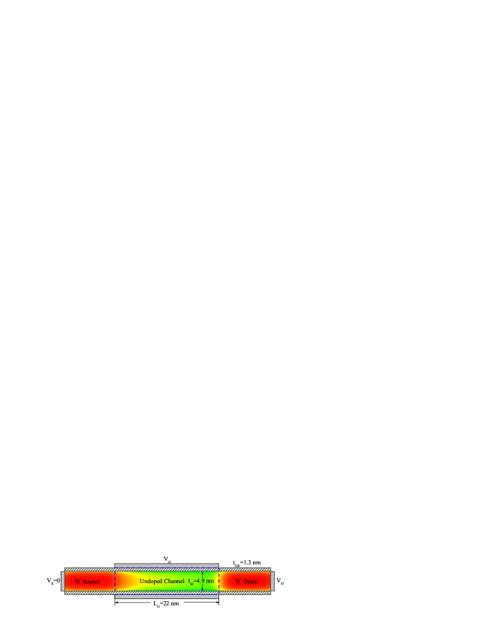
III Simulation for 22-nm double gate ultra-thin-body field-effect transistor
Following the ITRS 22 nm technology node, we present a three-dimensional atomistic quantum mechanical simulation on a 22 nm double gate ultra-thin-body field-effect transistor using the above presented three-dimensional TBS model. Previously, this kind of nanodevice has been studied by a TB and NEGF approach Luisier08 . Here, to achieve a comparison between our TBS model and NEGF model, we use the same structural and material parameters as in Ref. 41. Fig. 6 shows the structure and parameters of the simulated device. The channel direction is along (100). The gate length and silicon body thickness is nm and nm respectively. The thickness of the oxide is nm. The channel region is undoped while the source and drain region is highly doped as . The drain bias is fixed to be in the simulation. The Schrödinger equation (1) is solved in the whole device region with 0.8 million atoms using the LCBB method. An artificial periodic boundary condition is used connecting the left and right ends of the device with an artificial potential barrier between them. The resulting eigen states are occupied by the source/drain Fermi-Levels by the three-dimensional algorithm in the previous section. Then the occupied electron density is used in the Poisson equation (2) to form a self-consistent calculation. The Poisson equation (2) is only solved within the box of the blue dashed line shown in Fig.6. A typical Pulay DIIS charge mixing iteration scheme is used to accelerate the speed of the self-consistent calculation. For more details for how to solve the Poisson equation and its boundary conditions, please see Ref.Jiang09, . In the LCBB calculation, k-points are chosen from six X-valleys (two X100, two X010 and two X001) and in total there are about 7000 k-points included in the LCBB expansion. Two conduction bands are selected in the LCBB basis set. The calculation is carried out on a computer with a single CPU.
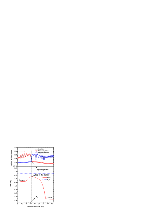
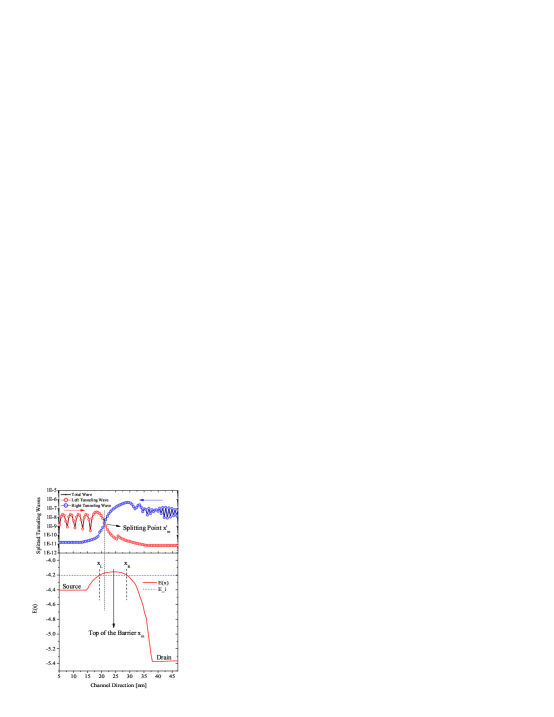
Fig. 7 and 8 shows how the TBS works for such LCBB calculated million atom 3D system. For ballistic and tunneling case, the black solid line in Figs. 7 and 8 indicates the total wave of the eigen state while the red and blue lines with symbols indicate the right and left running (tunneling) waves. As can be seen from the figure, the two separated parts coincide very well with the total wave function at both side of the barrier. For the ballistic case as shown in Fig. 7, the right running and left running waves are separated at the top of the barrier and then are injected ballistically into the other sides of the barrier. For the tunneling case as shown in Fig. 8, the right and left tunneling waves separate at the minimum wave function point, then decay exponentially to the other side of the barrier. Note that unlike in the 1D case shown in Figs.1 to 3, the potential profile in the 3D case, hence the potential maximum point depends on the state index i. Nevertheless, the separating algorithm remains the same.
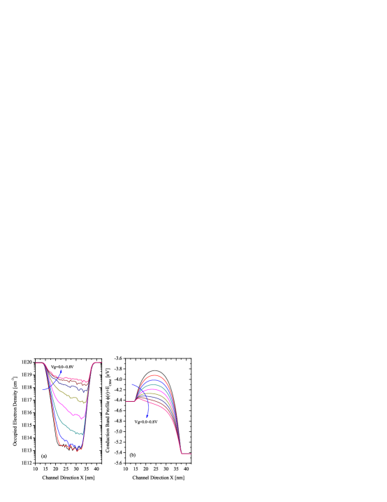
Fig. 9 shows the converged occupied electron density and local conduction band profile (which equals ) for . As can be seen from the figure, in low gate voltage cases, the electron density decays very fast from the source/drain to the channel. The electron density at small gate bias decays order from the source/drain region to the channel region. As the gate bias gets higher, the barrier in the channel is pushed down leading to a significantly increased charge density in the channel. It should be noted that the maximum point of the barrier moves towards the source side as the gate potential further pushes the barrier down.
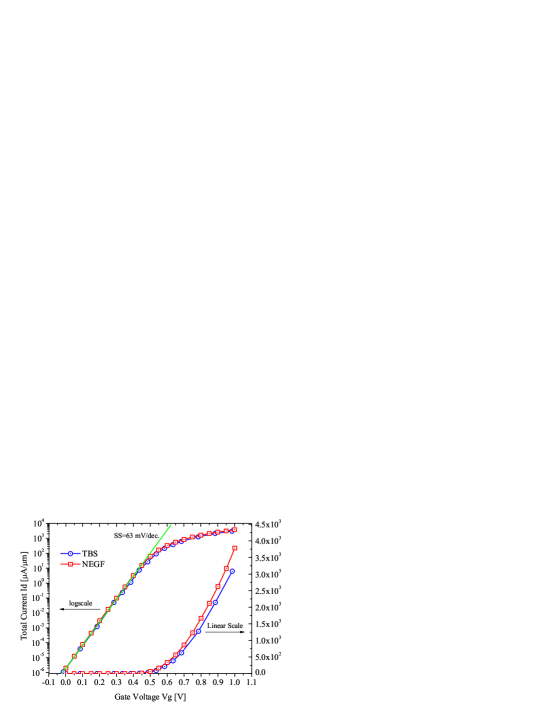
Finally, Fig. 10 compares the I/V curves of our splitting model and the NEGF incorporated tight-binding model Luisier06 ; Luisier08 . The I/V data of the TB+NEGF model is from Ref.41. Despite of the different Hamiltonians used, and different numerical details in solving the Poisson equations, the results aggree excellently. Table.I gives a detailed comparison of some key device performance parameters. As can be seen from the table, there is just a difference between the ON currents of the two models and only 10 mV difference between the threshold voltages. Both two models give exactly the same sub-threshold swing which is defined as in sub-threshold region. This value () is close to the theoretical limit of , indicating a very effective gate control in such a double-gate ultra-thin-body device.
Note that the TB+NEGF model solves the transport problem based on an open boundary condition while our splitting model is based on a periodic boundary condition and solves the same problem from the eigen states. From the comparisons, we see that these two methods lead to almost the same results. However, the computational costs for these two models are significantly different, while thousands of computer processors are used for the TB+NEGF approach, a single processor is used for our TBS approach. Overall, this is an evidence of the validity of our TBS model for 3D systems.
IV Summary
In summary, we have presented a new empirical pseudopotential calculation approach to simulate million atom nanostructure semiconductor devices using the periodic boundary conditions. To treat the non-equilibrium condition, instead of calculating the scattering states from the source and drain, we calculated the stationary states by the linear combination of bulk band method and then separated the whole wave function into source and drain parts according to a top of the barrier splitting (TBS) scheme based on the physical insight of ballistic and tunneling transport. The separated electronic states were then occupied according to the source/drain Fermi-Levels to yield the occupied electron density which is then used in the Poisson Equation solver to form a self-consistent calculation. The validity of TBS was verified by a comparison between the TBS calculation and scattering states calculation in a 1D effective mass model. It is also verified by comparing our LCBB-TBS calculation for a 3D double-gate field-effect transistor with a non-equilibrium Green’s function tight-binding result. However, instead of using thousands of processors, our method can be calculated using a single processor. Thus, this method provides a fast way to simulate the non-equilibrium million atom nanostructure problems.
Acknowledgment
This work was supported by the National Basic Research Program of China (973 Program) grant No. G2009CB929300 and the National Natural Science Foundation of China under Grant Nos. 60821061 and 60776061. L.W.W is funded by the U.S. Department of Energy BES, office of science, under Contract No. DE-AC02-05CH11231.
References
- (1) International Technology Roadmap for Semiconductors. Available at http://public.itrs.net.
- (2) M. Ieong, B. Doris, J. Kedzierski, K, Rim, and M. Yang, Science vol.306, pp.2057-2060, 2004.
- (3) Y. Taur, IBM J. RES. & DEV. vol.46, no.2/3, pp.213-221, 2002.
- (4) T. Hiramoto, M. Saitoh and G. Tsutsui, IBM J. RES. & DEV. vol. 50, no. 4/5, pp.411-417, 2006.
- (5) H. Iwai, Solid-State Electronics, vol.48, pp.497-503, 2004.
- (6) Scott Roy and Asen Asenov, Science vol.309, pp.388-390, 2005.
- (7) M. Shin, J. Appl. Phys. 101, 024510 (2007).
- (8) M.P. Anantram, A. Svizhenko, IEEE Trans. Elec. Dev. 54, 2100 (2007).
- (9) V. Sverdlov, E. Ungersboeck, H. Kosina, S. Selberherr, Mat. Sci. Eng. R58, 228 (2008).
- (10) G.J. Iafrate, H.L. Grubin, and D.K. Ferry, J. Phys. 42, 307 (1981).
- (11) D.K. Ferry and J.-R. Zhou, Phys. Rev. B 48, 7944 (1993).
- (12) S. Jin, M.V. Fischetti, T.-W. Tang, Appl. Phys. Lett. 92, 082103 (2008).
- (13) D. Vasileska, D.K. Ferry, S.M. Goodnick, Chapter 1, in Handbook of Theoretical and Computational Nanotechnology, Vol.10, Edited by: M. Rieth, W. Schommers (American Scientific Publications, California, USA, 2006).
- (14) R. Lake, G. Klimeck, R.C. Bowen, D. Javanovic, J. App. Phys. 81, 7845 (1997).
- (15) M. Luisier, A. Schenk, W. Fichtner, and G. Klimeck, Phys. Rev. B 74, 205323 (2006).
- (16) M. Luisier, G. Klimeck, IEEE EDL 30, 602 (2009).
- (17) C. Lent, D. J. Kirkner, J. Appl. Phys. 67, 6353 (1990).
- (18) G. Curatola, G. Fiori, G. Iannaccone, Solid State Elect. 48, 581 (2004).
- (19) A. Trellakis, A.T. Galick, A. Pacelli, U. Ravaiolli, J. App. Phys. 81, 7880 (1997).
- (20) A. Abramo, IEEE Trans. Elec. Dev. 47, 1858 (2000).
- (21) T. Hanajiri, et.al. Comp. Mat. Sci. 30, 235 (2004).
- (22) C. de Falco, E. Gatti, A.L. Lacaita, R. Sacco, J. Comp. Phys. 204, 533 (2005).
- (23) D.J. Frank, S.E. Laux, M.V. Fischetti, IEDM Tech. Dig. 13-16, 553 (1992).
- (24) A. Rahman, J. Guo, S. Datta, M.S. Lundstrom, IEEE TED 50, 1853 (2003).
- (25) A. DiCarlo, Semicond. Sci. Technol. 18, R1 (2003).
- (26) M. Bescond, J. L. Autran, D. Munteanu, and M. Lannoo, Solid-State Electron.
- (27) J. Wang, E. Polizzi, and M. S. Lundstrom, J. Appl. Phys. 96, 2192 (2004).
- (28) D. Esseni and P. Palestri, Phys. Rev. B 72, 165342 (2005).
- (29) N. Neophytou, A. Paul, M.S. Lundstrom, G. Klimeck, IEEE TED 55, 1286 (2008).
- (30) F. Sacconi, M. Povolotskyi, A. Di Carlo, P. Lugli, M. Stadele, Sol. Stat. Electron. 48, 575 (2004).
- (31) L. W. Wang and A. Zunger, Phys. Rev. B 59, 15806 (1999).
- (32) A.J. Williamson, L.W. Wang, A. Zunger, Phys. Rev. B 62, 12963 (2000).
- (33) J. W. Luo, S. S. Li, J. B. Xia and L. W. Wang, Appl. Phys. Lett. 90, 143108 (2007).
- (34) X. W. Jiang, H. X. Deng, S. S. Li, J. W. Luo and L. W. Wang, J. Appl. Phys. 106, 084510 (2009).
- (35) L.W. Wang, A. Zunger, J. Phys. Chem. 98, 2158 (1994).
- (36) S.M. Sze, ”Physics of Semiconductor Devices” (J. Wiley & Sons Inc. 2002).
- (37) A. Asenov, G. Slavcheva, A. R. Brown, J. H. Davies and S. Saini, IEEE Trans. Electron Devices 48, 722 (2001).
- (38) G. Kresse, J. Furthmuller, Comp. Mat. Sci. 6, 15 (1996).
- (39) http://www.pdesolution.com
- (40) A. Garcia-Lekue, L.W. Wang, Comp. Mat. Sci. 45, 1016 (2009).
- (41) M. Luisier and G. Klimeck, 10.1109/SISPAD.2008.4648226, Page(s): 17-20.
- (42) C. Jirauschek, IEEE J. Quan. Ele. 45, 1059 (2009).


| TBS | TB+NEGF | |
|---|---|---|
| () | 3265 | 3740 |
| (mV) | 460 | 450 |
| S (mV/dec.) | 63 | 63 |