Conduction of DNA molecules attached to a disconnected array of metallic Ga nanoparticles.
Abstract
We have investigated the conduction over a wide range of temperature of DNA molecules deposited across slits etched through a few nanometers thick platinum film. The slits are insulating before DNA deposition but contain metallic Ga nanoparticles, a result of focused ion beam etching. When these nanoparticles are superconducting we find that they can induce superconductivity through the DNA molecules, even though the main electrodes are non superconducting. These results indicate that minute metallic particles can easily transfer charge carriers to attached DNA molecules and provide a possible reconciliation between apparently contradictory previous experimental results concerning the length over which DNA molecules can conduct electricity.
pacs:
81.07.Nb,81.07.Gf,74.45.+cConductivity of DNA is a long-standing debate. Following the initial predictions that DNA molecules should conduct electricity, several types of experiments were attempted to probe the conduction mechanisms, ranging from emission and absorption spectroscopies barton1 to microwave absorption rf . Several groups have also attempted direct measurements of DNA conductivity by attaching DNA molecules to metallic electrodes porath1 ; fink . The contradictory experimental results, with behaviors ranging from insulator to coherent quantum transport over distances in the hundred nanometer range led to a strong controversy endres . The picture emerging in the past few years has been that DNA can conduct over distances of tens of nanometers: this was shown by STM and local probe techniques porath ; elke ; bingqian ; wang , as well as in a spectacular experiment barton : a nanometer long DNA molecule was inserted in a cut carbon nanotube, increasing its initial resistance only twofolds, and was subjected to biological manipulations that altered and then restored the conductivity. The importance of the environment of the molecules in order to have reproducible results was pointed out in mahapatro09 . Conduction over hundreds of nanometers, and up to several microns, was also reported by different groups okahata ; fink ; hartzell ; heim , including ours. In our previous experiments DNA was found to be conductive between platinum-carbon electrodes klinov and between rhenium-carbon electrodes kasumov . In this last case as the samples were lowered below the superconducting critical temperature of the electrodes (rhenium is a superconductor with ) the sample resistance decreased, indicating coherent quantum transport through the DNA molecules. These results are both technologically and fundamentally important since long range transport in DNA molecules may lead to the creation of new nanoscale self-assembled electronic devices. From the fundamental point of view, DNA is one of the rare one-dimensional molecular wires that can be obtained in mono dispersed form with known chemical structure and chirality. It is thus important to understand the ingredients that lead to conduction over long distances.
In this Letter we reconcile previous findings by showing that conduction over distances greater than hundreds of nanometers can occur if the DNA molecules are attached to a disconnected array of nanoparticles (typically 10 to 20 nm apart) that locally dopes the molecules, enhancing conduction. In addition in our case the nanoparticles are superconducting, which induces superconducting correlations in DNA at low temperatures.
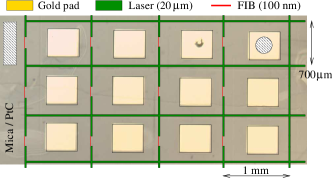
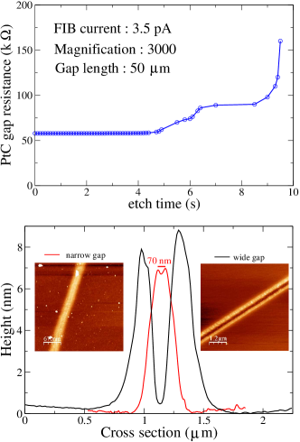
All our samples, including the previous ones, are fabricated with unconventional techniques: without electron beam lithography and with functionalization of the sample surface by a pentylamine plasma. Pentylamine was used because it is known to promote attachment of DNA to amorphous carbon films (such as those used in transmission electron microscopy, see dubochet ). The samples we describe hereafter are also fabricated using focused ion beam etching of a thin platinum carbon film deposited on mica, with subsequent pentylamine plasma treatment before deposition of DNA. Compared to our previous experiments we have gained a better understanding of this functionalization technique, establishing that pentylamine adheres only on carbonated surfaces and not directly on mica or metals. Thus fabrication begins with a mica substrate covered by a e-gun deposited platinum carbon film a few nanometers thick (5 nm thick, square resistance 1 kOhms). Although the carbon concentration is not known exactly, we checked that the concentration was high enough to anchor the pentylamine, since no DNA attached to a platinum surface without co-deposited carbon. We deposit thick gold contact pads through a mechanical mask and divide the centimeter square mica substrate into roughly twelve sample regions using a UV laser with a 30 micron diameter laser beam,see Fig.1. We then proceed to etch away the metal over a thin, long, region using a focused ion beam (magnification and current ). In order to obtain narrow insulating regions we monitor the resistance of a first slit as we etch the platinum film one line-scan at a time. We stop the etching as soon as the resistance diverges, see Fig.1. The other slits are etched using a slightly larger (15%) number of scans than was necessary to open the first slit. We then check electrically with a probe station that all slits have a resistance above a few G. The width of the slits fabricated with this technique ranges between 70 and 150 nm. The next step is pentylamine deposition, in a DC plasma discharge with pentylamine vapor pressure Torr, and current mA for a few minutes. A drop of -DNA dna solution was incubated on the substrate surface for a few minutes and then rinsed away using a water flow created by a peristaltic-pump (flow few cm/s). Out of eight mica substrates on which DNA deposition was attempted orsaymoscou , five were covered by DNA molecules as established by atomic force microscopy. These five substrates contained around 30 slits. All samples on two of these substrates were completely insulating. On the other three substrates 11 out of 15 samples were conducting. We have also prepared a control substrate, incubated with the same buffer but without DNA molecules, and rinsed like the other samples. We found that all 14 slits etched on these samples remained insulating.
Room temperature conductance was measured in a probe station, using an ac voltage in the mV range at frequencies ranging from 1 to 30Hz. The resistance of conducting samples was found to vary, depending on the slit, between 5 k and 50 k. These values are consistent with previous findings kasumov ; klinov , given that the number of deposited molecules across each slit varies between 10 and 100.
The pentylamine plasma creates a positively charged organic layer that allows DNA molecules to bind to the carbonated hydrophobic electrodes. Conducting AFM characterization of this pentylamine layer on a smooth Pt/C film indicates that the pentylamine film forms a smooth insulating layer. This is not the case along the edge of the slits, where FIB etching as well as unavoidable carbon contamination introduce roughness, leading to defects and holes in the pentylamine coverage. As a result the edges of the slit remain metallic, as is needed to establish electrical contact to the DNA on both sides of the slit.
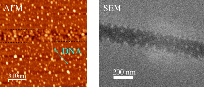
We have used both atomic force atomic microscopy and high resolution scanning electron microscopy to characterize the structure of the FIB etched slit. We find that the insides of the slits are rather rough for two reasons: The incomplete etching of the platinum film leaves metallic disconnected islands of typical size 10 nanometers. In addition, some slits contain a disordered array of roughly spherical nanoparticles (see Fig.2). The regular shape of these spheres contrasts with the irregular shape of the etching residues of PtC. As confirmed by transport experiments presented below, these spherical nanoparticles result from condensed gallium drops generated by the FIB. Their size varies between 3 and 10 nm, their separation between 5 and 20 nm. Even if these nanoparticles do not directly contribute to electronic transport through the slits, which were insulating before deposition of DNA and remained so after a flow of saline buffer solution without molecules, we will see that they certainly modify the electronic properties of DNA molecules deposited across the slit.
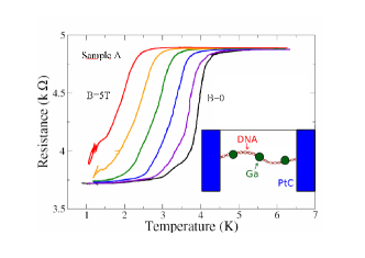
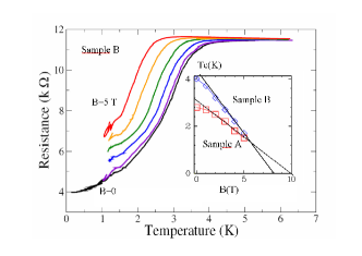
In the following we present low temperature transport measurements of DNA molecules deposited through slits decorated with gallium nanoparticles. The samples investigated have resistances ranging from 5 to 20 at room temperature, with roughly 10 to 30 connected molecules, as deduced from the density of molecules on the substrate far from the slit. The samples were electronically and mechanically connected by gold plated spring contacts fragile on the gold pads on the Pt/C film, and mounted in a dilution refrigerator operating down to 50 mK. The resistance was measured via lines with room temperature low pass filters. Measurements were performed in a current biased configuration using an ac current source of 1 nA operating at 27 Hz and a Lock-in detector with a low noise voltage pre-amplifier. Whereas the resistance was nearly independent of temperature between room temperature and 4 K, it dropped as T decreased, with a broad transition to a value of the order of 4 (which corresponds to the resistance of the normal Pt/C electrodes in series with the DNA molecules), see Fig. 3. This transition to partial proximity-induced superconductivity is shifted to lower temperatures in a magnetic field. It is the broadest for the most resistive sample, and exhibits the smallest magnetic field dependence.
Another superconducting-like feature is the non linear IV curves at low temperature, see Fig. 4: The dc current-dependent differential resistance is lowest at small dc current and increases with increasing dc current. The increase is non monotonous, presenting several peaks up to a current of the order of , a sort of critical current, above which the resistance is constant and independent of dc current. The many peaks in the differential resistance curves are typical of non homogeneous superconductivity. For instance the differential resistance jumps seen in narrow superconducting wires (diameter smaller than coherence length) are associated with the weak spots of the wire. Since neither the Pt/C electrodes nor the DNA molecules are superconducting (as shown in previous experiments), these results suggest that the gallium nanoparticles, which are superconducting, induce superconductivity through the DNA molecules. The superconducting transition temperature of pure gallium is but it is reasonable to expect that the gallium nanoparticles, because of their small size and their probable large carbon content, have a higher tcgallium . It is interesting to note that the low intrinsic carrier density in the DNA molecules may prevent the inverse proximity effect, i.e. the destruction of the superconductivity of the gallium nanoparticles. Those same nanoparticles could not induce any proximity effect in metallic wires because of the high density of carriers in metals. This possibility of inducing long range superconductivity with superconducting nanoparticles was investigated recently in the context of graphene kostya . In the present case, it is also possible that the gallium nanoparticles could contribute to carrier doping of the DNA molecules in the normal state.
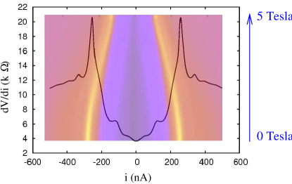
The difference between the transitions of the various samples is probably related to the existence of nanoparticles of different sizes, leading to superconducting transitions more rounded and with a weaker dependence in small particles than in large ones. The radius of the nanoparticles inducing superconductivity in DNA can be estimated from the critical field , for which the transition temperature extrapolates to 0. This field (see Fig.3) is of the order of 10 T, corresponding to a radius between 5 and 7 nm. A rough estimate of the number of nanoparticles bound to DNA molecules participating in transport can also be deduced from the number of peaks of differential resistance which varies from 3 to 6 depending on the samples (the largest number of peaks is observed in the lowest resistance samples). This corresponds to a typical distance between nanoparticles attached to a DNA molecule of the order of 10 to 20 nm, which is thus the length over which we probe electronic transport along the DNA molecules, and not the total width of the slit. The relatively low values of measured resistances, as well as the appearance of proximity induced superconductivity, indicates a strong electronic coupling between the DNA molecules and both Pt/C residues and Ga nanoparticles. This contrasts with previous measurements of DNA molecules linking gold nanoparticles nanoau , where the conductivity did not exceed Scm-1 for a distance between metallic nanoparticles of 10 nm, whereas the conductivity in the present case can be estimated to be of the order of unity in the same units. Accordingly transport experiments on completely metallised DNA moleculesivan did not seem to indicate any intrinsic contribution of the DNA molecules to the conduction measured. These differences may originate in the nature of the binding between the metallic nanoparticles and the DNA which in ref. nanoau was of covalent nature (involving alkanethiol molecules of low conductivity), whereas in the present case we believe that a good electrical contact between DNA molecules and the metallic nanoparticles is provided by the discontinuities and defects in the pentylamine film.
Our results indicate that minute metallic particles can transfer charge carriers to attached DNA molecules and confirm that DNA molecules can be conducting on lengths of the order of 10 nm but we cannot conclude with these experiments on the conduction on longer length scales. Since in our previous experiments kasumov ; klinov the DNA molecules were connected across similarly etched slits in thin metallic films, the existence of metallic residues cannot be excluded, and the conduction of DNA molecules could thus also have been probed on distances no greater than 10 nm. These results invite to a systematic investigation of the possible carrier doping of DNA by metallic nanoparticles.
We thank F. Livolant, A. Leforestier, D. Vuillaume and D. Deresmes for fruitful discussions and acknowledge ANR QuantADN and DGA for support.
| # of substrates | 12 |
|---|---|
| # of FIB slits | 100 |
| # of substrates with visible DNA | 5 |
| # of substrates with conducting slits after deposition | 3 |
| # of slits on these 3 substrates | 15 |
| # of conducting slits after deposition | 11 |
| # of slits on the control sample | 14 |
| # of conducting slits after buffer | 0 |
References
- (1) M. R. Arkin, E. D. A. Stemp, R. E. Holmlin, J. K. Barton, A. Hoermann, E. J. C. Olson, and P. F. Barbara Science 273, 475 (1996), D. B. Hall, R. E. Holmlin, and J. K. Barton, Nature, 382, 731 (1996).
- (2) P. Tran, B. Alavi and G. Gruner, Phys. Rev. Lett. 85 1564 (2000).
- (3) H.-W Fink and C. Schönenberger, Nature 398 407 (1999)
- (4) D. Porath, A. Bezryadin, S. de Vries and C. Dekker, Nature 403 635 (2000)
- (5) R.G. Endres, D.L. Cox and R.R.P. Singh, Rev. Mod. Phys. 76, 195 (2004)
- (6) Xuefeng Guo, Alon A. Gorodetsky, James Hone, Jacqueline K. Barton and Colin Nuckolls, Nature Nanotechnology 3, 163 (2008).
- (7) Bingqian Xu, Peiming Zhang, Xiulan Li,and Nongjian Tao, Nano. Let. 4, 1105 (2004).
- (8) N. Kang, A. Erbe, and E. Scheer, New J. Phys. 10, 023030 (2008),App. Phys. Let. 96, 023701 (2010).
- (9) Errez Shapir, Hezy Cohen, Arrigo Calzolari, Carlo Cavazzoni, Dmitry A. Ryndyk, Gianaurelio Cuniberti, Alexander Kotlyar, Rosa Di Felice and Danny Porath, Nature Materials 7, 68 (2008)
- (10) J.Wang B 78, 245304 (2008).
- (11) Y.Okahata et al. Supramol.Sci. 5,317 (1998).
- (12) B. Hartzell et al. J. Appl. Phys.,94 , 2764 (2003)
- (13) T. Heim, D. Deresmes, and D. Vuillaume, Appl. Phys. Lett. 85, 2637 (2004) , T. Heim, D. Deresmes, and D. Vuillaume, J. Appl. Phys. 96, 2927 (2004).
- (14) AK Mahapatro, GU Lee, KJ Jeong, DB Janes - Appl. Phys. Let.95, 083106 (2009).
- (15) A. Yu. Kasumov, M. Kociak, S. Guéron, B. Reulet, V. T. Volkov, D. V. Klinov and H. Bouchiat, Science 291 280 (2001).
- (16) A. Yu. Kasumov, D. V. Klinov, P.-E. Roche, S. Guéron, and H. Bouchiat, App. Phys. Lett. 84 1007 (2004);
- (17) The DNA solution was prepared with a commercial solution: ”Invitrogen Cat no. 25250-028” in Tris-HCl (pH 7.4), 10 mM and 5 mM EDTA 0.1 mM diluted in a magnesium chloride buffer 15 mM and 5 mM.
- (18) J. Dubochet, M. Ducommun, M. Zollinger and E. Kellenberger J. Ultrastruct. Res. 35 147 (1971)
- (19) Plasma functionalization and DNA deposition were attempted at two different laboratories, but conducting samples were obtained only in the setup in Moscow. Thus electrical measurements were performed in Orsay several days later.
- (20) Standard connecting techniques such as ultrasonic or silver paste bonding destroyed the conductivity of some of the samples.
- (21) M.V. Feigel’man, M.A. Skvortsov and K.S. Tikhonov, Solid State Comun. 1101 (2009)
- (22) O. N. Bakharev et al Phys. Rev. Lett. 96, 117002 (2006).
- (23) So-Jung Park et al Angew. Chem. 3845,39(2000).
- (24) E Braun, Y Eichen, U Sivan and G Ben-Yoseph Nature 391 776,(1998).