Long electron dephasing length and disorder-induced spin-orbit coupling in indium tin oxide nanowires
Abstract
We have measured the quantum-interference magnetoresistances in two single indium tin oxide (ITO) nanowires between 0.25 and 40 K, by using the four-probe configuration method. The magnetoresistances are compared with the one-dimensional weak-(anti)localization theory to extract the electron dephasing length . We found, in a 60-nm diameter nanowire with a low resistivity of (10 K) = 185 cm, that is long, increasing from 150 nm at 40 K to 520 nm at 0.25 K. Therefore, the nanowire reveals strict one-dimensional weak-localization effect up to several tens of degrees of Kelvin. In a second 72-nm diameter nanowire with a high resistivity of (10 K) = 1030 cm, the dephasing length is suppressed to (0.26 K) = 200 nm, and thus a crossover of the effective device dimensionality from one to three occurs at about 12 K. In particular, disorder-induced spin-orbit coupling is evident in the latter sample, manifesting weak-antilocalization effect at temperatures below 4 K. These observations demonstrate that versatile quantum-interference effects can be realized in ITO nanowires by controlling differing levels of atomic defects and impurities.
pacs:
73.63.-b, 73.23.-b, 73.20.Fz, 73.20.JcI Introduction
In weakly disordered metals and semiconductors (all real conductors are disordered), quantum-interference electron transport plays vital roles at liquid-helium temperatures Imry . The quantum-interference phenomena, which originate from the inherent wave nature of the conduction electrons, become progressively pronounced as the temperature is lowered and the effective device dimensionality is reduced. In this regard, metal and doped semiconductor nanowires could provide a rich platform for probing novel, nonclassical properties and functionalities. In a random potential, the conduction electrons undergo Brownian-type diffusive motion, leading to various quantum-interference phenomena, including the weak-(anti)localization effect, Aharonov-Bohm oscillations, universal conductance fluctuations, and persistent currents Nazarov . Previously, such quantum-interference behaviors have mostly been investigated by utilizing submicron devices fabricated via the ‘top-down’ electron-beam lithography technique Washburn86 .
Compared with the temperature dependence of the resistance rise due to weak-localization and electron-electron interaction effects at low temperatures Altshuler87 , magnetoresistances induced by small externally applied magnetic fields can provide very quantitative information about the inelastic electron (electro-phonon and electron-electron) scattering and spin-flip (spin-orbit and magnetic spin-spin) scattering mechanisms in a given nanowire device Lin-jpcm02 . Therefore, systematic and careful measurements of magnetoresistances in the weak-(anti)localization effect are indispensable and highly desirable for learning the responsible microscopic electron relaxation processes dephasing . Reliable knowledge about the electron relaxation processes can help in paving the way for the future realization of sensitive and versatile quantum-interference nanoelectronics and spintronics. Since as-grown metal and semiconductor nanowires often contain high levels of point defects Chiu-nano09ITO ; Chiu-nano09ZnO , it is natural to expect that quantum-interference effects should be pronounced in many ‘bottom-up’ nanostructures.
Among the numerous metallic nanowires, Sn-doped In2O3 (indium tin oxide or ITO) nanowires have recently been studied Wan06 ; LinD07 ; Dwyer09 . The interest in these nanoscale structures arises from the fact that the parent ITO material is a transparent conducting oxide. Moreover, the charge carriers in this material are established to be essentially free-electron-like Mryasov01 . That is, the charge carriers behave like an ideal free electron gas with an effective mass of and a small Fermi energy 1 eV, where is the free electron mass. The thermoelectric power reveals a linear diffusive term from 300 K all the way down to liquid-helium temperatures, while the temperature dependence of resistivity is well described by the Bloch-Grüneisen law at not too low temperatures Li-JAP04 . The carrier concentration in highly conductive ITO materials falls in the range – cm-3 Tahar98 , and the room temperature resistivity can be as low as 100–200 cm Wan06 . Therefore, ITO nanowires appear to be attractive candidates for in-depth investigations of the quantum-interference electron transport. Surprisingly, to the best of the authors’ knowledge, the weak-localization magnetoresistances in ITO nanowires has previously been reported only in one study in which the electrical measurements were performed on two-probe, rather than four-probe, individual nanowire devices Chiquito07 . In that experiment, the authors reported a very short electron dephasing (phase-breaking) length, , of 31 (15) nm at 10 (100) K.
In this work, we have investigated low-temperature magnetoresistances in the weak-(anti)localization effect in one low-resistivity and one high-resistivity ITO nanowires, by employing the four-probe configuration method. The electron dephasing length and the spin-orbit scattering length, , are experimentally extracted. We found a very long (0.25 K) 520 nm, which is considerably longer than most electron dephasing lengths reported in previous studies of as-grown nanowires. Furthermore, we demonstrate that the strength of spin-orbit coupling can be adjusted by modifying the level of disorder or electron mean free path, , in the nanowire. As a consequence, both the weak-localization effect (which is characterized by negative magnetoresistances) and the weak-antilocalization effect (which is characterized by positive magnetoresistances) can be ‘tuned’ and visualized in ITO single nanowires in low magnetic fields.
II Experimental method
ITO (In2-xSnxO3-y) nanowires were synthesized on Si substrates by the standard thermal evaporation method, as described previously Chiu-nano09ITO . X-ray diffraction (XRD, MAC Science MXP-18) and high-resolution transmission electron microscopy (TEM, JEOL JEM-2010FX) studies indicated that the nanowires were single crystalline, possessing a cubic bixbyite structure, and grew along the [100] direction. Energy dispersive x-ray spectroscopy (EDS, JOEL JEM-2010FX) and inductively coupled plasma atomic emission spectrometry (ICP-OES, Perkin Elmer Optima-3000DV) were utilized to determine the chemical compositions of the nanowires. We obtained an Sn/In weight ratio of 4.4%, confirming that Sn was effectively incorporated into the ITO nanowires Chiu-nano09ITO .
Both the electron-beam lithography and focused-ion beam (FIB) techniques were employed to make four-probe individual nanowire devices for magnetoresistance measurements. We first made micron-sized Ti/Au (10/60 nm) metal pads and coordinate marks by utilizing the standard photolithography and lift-off technique on a SiO2 layer (400 nm thick) capped Si substrates. ITO nanowires were then dispersed on the SiO2/Si substrates. Individual nanowires with diameters of 60–70 nm were identified and electrically connected to the pre-patterned micron-sized Ti/Au metal pads by using the standard electron-beam lithography and lift-off technique (for the ITO-r nanowire device). In order to make good ohmic contacts to the nanowire, O2 plasma was employed to clean the substrate before the Cr/Au (10/100 nm) electrodes contacting the nanowire were deposited by the thermal evaporation method. A scanning electron microscope (SEM) image of the ITO-r nanowire is shown in the inset of Fig. 2.
To fabricate the four-probe ITO-f individual nanowire device, we employed the FIB technique. In an FEI Dual-Beam NOVA 200 FIB instrument, we applied the Ga+-beam-induced deposition method with a methyl cyclopentadienyl trimethyl platinum (CH3)3Pt(CpCH3) injector to selectively deposit Pt metal for connecting the ITO nanowire with the Ti/Au pads. The Ga+-ions were accelerated to 30 kV at 10 pA and injected into the nanowire during the Pt deposition. The dimensions of the Pt contacting electrodes were set 80 nm in width and 100 nm in thickness, but the actual width was about 300 nm and the actual thickness was not determined. An SEM image of the four-probe ITO-f nanowire device is shown in the inset of Fig. 4.
The individual nanowire devices were placed on a sample holder which was situated inside a dark vacuum can. The vacuum can was mounted on an Oxford Heliox 3He cryostat for magnetoresistance measurements from 40 K down to 0.25 K. The cryostat was equipped with a 4-T superconducting solenoid, and the temperature was monitored with calibrated RuO2 and Cernox thermometers. An AC resistance bridge (Linear Research LR-700) was employed for the measurement of magnetic field dependent resistance, , at various fixed temperatures. In all cases, the magnetic fields were applied perpendicular to the nanowire axis. A small measuring current ( 30 nA) was employed to avoid Joule heating. Linearity in the current-voltage curves was repeated checked and ensured.
III Results and discussion
Figure 1 shows the normalized magnetoresistance, , as a function of magnetic field at several temperatures of the low-resistivity ITO-r nanowire. This figure reveals that the magnetoresistances are always negative, implying a very weak spin-orbit scattering rate relative to the inelastic electron scattering rate even down to 0.25 K in this particular nanowire. Our measured low-field magnetoresistances were least-squares fitted to the one-dimensional weak-localization theoretical prediction Altshuler87 ; Birge03
| (1) | |||||
where is the resistance of a nanowire of width and length , is the magnetic length ( is the Planck constant divided by , and is the electronic charge), is the electron dephasing length, is the spin-orbit scattering length, and is the electron diffusion constant diffusion ( being the Fermi velocity Fermi , and being the electron mean free time). Here and are the electron dephasing time and the spin-orbit scattering time, respectively. The spin-orbit scattering length (time) is a temperature independent quantity whose size, relative to the inelastic scattering strength, determines the sign of the weak-(anti)localization effects in the low-field magnetoresistance Altshuler87 ; Bergmann82 .
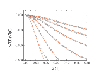
In Fig. 1, the symbols are the experimental data and the solid curves are the theoretical predictions of Eq. (1). This figure clearly indicates that the measured magnetoresistances can be well described by the one-dimensional weak-localization theory in the wide temperature interval of 0.25–40 K. Therefore, the important characteristic electron scattering lengths, and , can be accurately extracted. In this low-resistivity nanowire, we obtained an extraordinarily long (). In other words, the spin-orbit interaction is negligibly weak (absent), to within our experimental uncertainty, in this sample. [We estimate the length 0.5 m, or the time s, in this nanowire (see below). It is worth noting that this spin-orbit scattering length is comparable to or even longer than that in relatively clean Al films and wires Santhanam87 .]
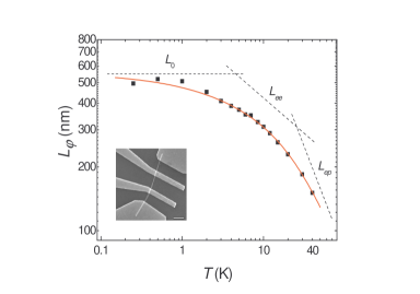
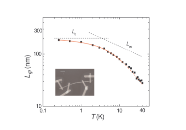
Figure 2 shows our extracted as a function of temperature for the low-resistivity ITO-r nanowire. The inset shows an SEM image of this individual nanowire device. This figure indicates that increases from 150 nm to 520 nm as the temperature decreases from 40 K down to 0.25 K wire-length . This result bears significant implications. As a consequence of such a long , the weak-localization behavior is purely one-dimensional in this particular nanowire device over our whole measurement temperature range. In fact, it is clear that the one-dimensional weak-localization behavior will persist up to much above 40 K. In contrast, in previous studies of individual nanowires made of ITO Chiquito07 ; Berengue09 , and other materials such as InAs Liang09 ; Liang10 and P-doped Si Rueb-prb07 , the magnetoresistance measurements were performed on two-probe configurations and the obtained were often short ( 100 nm at 1 K). Thus, a crossover of the device dimensionality from one to three, in regard to the weak-localization effect, inevitably happens already at low temperatures of a few degrees of Kelvin. Under such circumstances, the extracted values of () above a few degrees of Kelvin are obviously questionable.
| Sample | (300 K) | (10 K) | ||||||||
|---|---|---|---|---|---|---|---|---|---|---|
| (nm) | (m) | ( cm) | ( cm) | (nm) | (cm2/s) | (fs) | (ps) | (ps) | (K-2 s-1) | |
| ITO-r | 60 | 1.5 | 202 | 185 | 9.3 | 25 | 12 | 100 | 120 | |
| ITO-f | 72 | 2.8 | 997 | 1030 | 2.9 | 5.9 | 4.2 | 26 | 69 |
In a weakly disordered conductor, the electron dephasing time is given by Lin-jpcm02
| (2) |
where is a constant, whose origins (paramagnetic impurity scattering, dynamical structural defects, etc.) are a subject of elaborate theoretical and experimental investigations Birge03 ; Lin-prb87b ; Mohanty97 ; Lin-JPSJ03 ; Huang-prl07 . The electron-electron relaxation rate, , in low-dimensional disordered conductors is known to dominate in an appreciably wide temperature interval Altshuler87 ; Lin-jpcm02 . The electron-phonon scattering rate, , will become important at high measurement temperatures. We use the standard expression: in the quasi-ballistic limit of (which is pertinent to the present study) Sergeev-prb00 ; Zhong-prl10 , where is the wavenumber of a thermal phonon and is the electron mean free path. The electron-electron relaxation rate was fitted in the form . As it is shown in Fig. 2, the dependence is well fitted by Eq. (2) with four adjustable parameters , , , and . Our fitted values of and are listed in Table 1. It should be stressed that we obtain an exponent of temperature , which is very close to the theoretical value (= 2/3) of the Nyquist electron-electron scattering rate in one dimension. Moreover, our fitted value of is in good agreement with the theoretical prediction of Altshuler87 ; Lin-jpcm02 ; Birge03
| (3) |
Equation (3) predicts a scattering rate with the coefficient K-2/3 s-1 in the ITO-r nanowire, while experimentally we obtain K-2/3 s-1. Also plotted in Fig. 2 are our fitted values of the three dephasing contributions , , and , as indicated. This figure indicates that the electron-phonon scattering becomes comparable to the electron-electron scattering at 25 K.
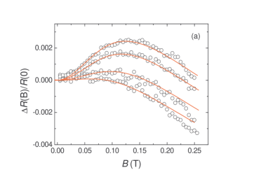
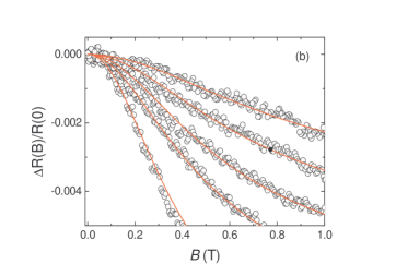
Figure 3(a) shows the normalized magnetoresistances of the high-resistivity ITO-f nanowire resistivity as a function of magnetic field at four temperatures between 0.26 and 4 K. Figure 3(b) shows the normalized magnetoresistances as a function of magnetic field at five temperatures between 8.5 and 40 K. These figures reveal that the magnetoresistances are negative in all fields at temperatures above 6 K. Nevertheless, below 4 K, the magnetoresistances are positive in low magnetic fields, changing to negative magnetoresistances in higher magnetic fields. The positive contribution is more pronounced at lower temperatures. This marked behavior can be readily understood in terms of the quantum-interference effect in the presence of a notable spin-orbit scattering rate relative to the inelastic electron-electron and electron-phonon scattering rates. Under such conditions, positive magnetoresistances arise owing to the weak-antilocalization effect Altshuler87 ; Lin-jpcm02 .
The presence of a notable spin-orbit scattering rate in the ITO-f nanowire can be explained as follows. In this nanowire, the resistivity [(10 K) = 1030 cm)] is considerably higher than that (185 cm) in the ITO-r nanowire. Therefore, the spin-orbit interaction in this nanowire should be significantly enhanced according to the (approximate) relation Santhanam87 ; Abrikosov ; Bergmann85 ; Bergmann10 : , where is the atomic number of the relevant scatterer. A comparatively high resistivity in the ITO-f nanowire implies a relatively short , which should lead to a large . Quantitatively, we obtain 125 nm in this nanowire (see below). The present experiment suggests that one can tailor both the weak-localization and weak-antilocalization effects in ITO nanowires by carefully controlling the level of atomic imperfections (point defects and/or heavy impurities). This observation provides valuable information about the feasible implementation of future quantum-interference nanodevices. In addition to a long dephasing length (leading to sensitive quantum transport effects), the capability of tuning spin-orbit coupling could be advantageous for the future realization of spintronic devices Zutic04 .
Our measured magnetoresistances in the ITO-f nanowire can be well described by the predictions of Eq. (1) [the solid curves in Figs. 3(a) and 3(b)], and the extracted as a function of temperature is plotted in Fig. 4. The inset shows an SEM image of this individual nanowire device. Inspection of Fig. 4 indicates that in this nanowire is considerably shorter than that in the ITO-r nanowire. This can be explained by the fact that is suppressed by a high level of disorder, i.e., a short mean free path, in the ITO-f nanowire. [Note that Eq. (3) predicts that , and in the quasi-ballistic limit Sergeev-prb00 ; Zhong-prl10 .] Our result was fitted to Eq. (2) (the solid curve in Fig. 4) and the adjustable values of and are listed in Table 1. Again, we obtain the exponent of temperature in , being very close to the theoretical value of 2/3. In addition, our fitted value of the one-dimensional electron-electron scattering coefficient K-2/3 s-1 is in excellent agreement with the theoretical prediction of K-2/3 s-1 from Eq. (3). Such close agreement between experiment and theory most likely arises from the intricate material fact that, though being a doped oxide, ITO possesses a free-carrier-like (i.e., parabolic) electronic band structure Chiu-nano09ITO ; Li-JAP04 ; Mryasov01 . We notice in passing that, in another high-resistivity nanowire with = 110 nm and (10 K) = 1690 cm, we obtained (0.25 K) = 170 nm and = 95 nm. These values are in good consistency with the corresponding values in the ITO-f nanowire.
It should be noted that in the ITO-f nanowire, our extracted value of becomes smaller than the nanowire diameter at a temperature of 12 K. That is, a dimensionality crossover of the weak-localization effect nominally begins to set in at 12 K in this particular nanowire device. Strictly speaking, the measured magnetoresistances should then be least-squares fitted with the three-dimensional weak-localization theoretical predictions Lin-jpcm02 ; Wu-prb94 in order to extract . However, we found that between 12 and 40 K, our measured magnetoresistances can still be satisfactorily described by Eq. (1) [see Fig. 3(b)], while the three-dimensional weak-localization theory does not apply 3D . In any case, the extracted value of above 12 K in this nanowire device should be considered only qualitative and treated with caution. (Hence, in Fig. 4, we only plotted our fitted values of the two contributions and .)
IV Conclusion
We have quantitatively measured the electron dephasing length in two individual ITO nanowires between 0.25 and 40 K. We observe that the electron dephasing length is very long, reaching 520 nm at 0.25 K in a low-resistivity ITO nanowire. As a consequence, the sample demonstrates strict one-dimensional weak-localization effect up to temperatures above 40 K. In a high-resistivity nanowire, the spin-orbit coupling is enhanced due to a short electron mean free path, manifesting the weak-antilocalization effect at temperatures below 4 K. These observations provide strong indications that robust quantum-interference effects can be realized, and tunable, in ITO nanowires by controlling differing levels of atomic defects and impurities.
Acknowledgements.
The authors are grateful to C. Y. Wu for careful reading of the manuscript, and F. R. Chen and J. J. Kai for providing us with the ITO nanowires used in this study. This work was supported by Taiwan National Science Council through Grant No. NSC 98-2120-M-009-004, and by the MOE ATU Program.References
References
- (1) Y. Imry, Introduction to Mesoscopic Physics (Oxford University Press, Oxford, 1997).
- (2) Y. V. Nazarov and Y. M. Blanter, Quantum Transport: Introduction to Nanoscience (Cambridge University Press, Cambridge, 2009).
- (3) S. Washburn and R. A. Webb, Adv. Phys. 35, 375 (1986).
- (4) B. L. Altshuler, A. G. Aronov, M. E. Gershenson, and Yu. V. Sharvin, Sov. Sci. Rev., Sect. A 9, 223 (1987).
- (5) J. J. Lin and J. P. Bird, J. Phys: Condens. Matter 14, R501 (2002).
- (6) Compared with other quantum-interference phenomena, the weak-(anti)localization method provides the most quantitative way for extracting the electron dephasing time (Refs. Lin-jpcm02, and Bergmann10, ).
- (7) S. P. Chiu, H. F. Chung, Y. H. Lin, J. J. Kai, F. R. Chen, and J. J. Lin, Nanotechnology 20, 105203 (2009).
- (8) S. P. Chiu, Y. H. Lin, and J. J. Lin, Nanotechnology 20, 015203 (2009).
- (9) Q. Wan, E. N. Dattoli, W. Y. Fung, W. Guo, Y. Chen, X. Pan, and W. Lu, Nano Lett. 6, 2909 (2006).
- (10) D. Lin, H. Wu, R. Zhang, and W. Pan, Nanotechnology 18, 465301 (2007).
- (11) C. O’Dwyer, M. Szachowicz, G. Visimberga, V. Lavayen, S. B. Newcomb, and C. M. S. Torres, Nature Nanotechnology 4, 239 (2009).
- (12) O. N. Mryasov and A. J. Freeman, Phys. Rev. B 64, 233111 (2001).
- (13) Z. Q. Li and J. J. Lin, J. Appl. Phys. 96, 5918 (2004).
- (14) R. B. H. Tahar, T. Ban, Y. Ohya, and Y. Takahashi, J. Appl. Phys. 83, 2631 (1998).
- (15) A. J. Chiquito, A. J. C. Lanfredi, R. F. M. de Oliveira, L. P. Pozzi, and E. R. Leite, Nano Lett. 7, 1439 (2007).
- (16) F. Pierre, A. B. Gougam, A. Anthore, H. Pothier, D. Esteve, and N. O. Birge, Phys. Rev. B 68, 085413 (2003); Y. Niimi, Y. Baines, T. Capron, D. Mailly, F. Y. Lo, A. D. Wieck, T. Meunier, L. Saminadayar, and C. Bäuerle, ibid. 81, 245306 (2010).
- (17) While our ITO nanowires are one-dimensional with regard to the quantum-interference weak-(anti)localization effect, they are three-dimensional with regard to the classical Boltzmann transport, i.e., the electron mean free path , the diameter of nanowire.
- (18) Our Fermi velocities were evaluated by using valus of = 0.7 and 0.4 eV in the ITO-r and ITO-f nanowires, respectively. See Refs. Chiu-nano09ITO, and Li-JAP04, .
- (19) G. Bergmann, Solid State Commun. 42, 815 (1982).
- (20) P. Santhanam, S. Wind, and D. E. Prober, Phys. Rev. B 35, 3188 (1987).
- (21) We note that, in the studies of short nanowires, the effect of measurement-probe geometry on one-dimensional weak-localization magnetoresistance should be treated with caution and may not be always neglected, see V. Chandrasekhar, D. E. Prober, and P. Santhanam, Phys. Rev. Lett. 61, 2253 (1988). In the present case, the ITO-r nanowire length at the lowest temperatures. The ratio is even larger at higher temperatures. In addition, our Ti/Au electrodes were deposited onto the ITO nanowire during separate lithography processes. There were “dirty” interfaces formed between the electrodes and the nanowire. All these factors will render the measuring probe effect less significant. We estimate the effect of measurement-probe geometry, if any exists, would cause a correction of less than a few percents to the present result.
- (22) O. M. Berengue, A. J. C. Lanfredi, L. P. Pozzi, J. F. Q. Rey, E. R. Leite, and A. J. Chiquito, Nanoscale Res. Lett. 4, 921 (2009).
- (23) D. Liang, M. R. Sakr, and X. P. A. Gao, Nano Lett. 9, 1709 (2009).
- (24) D. Liang, J. Du, and X. P. A. Gao, Phys. Rev. B 81, 153304 (2010).
- (25) F. J. Rueß, B. Weber, K. E. J. Goh, O. Klochan, A. R. Hamilton, and M. Y. Simmons, Phys. Rev. B 76, 085403 (2007).
- (26) J. J. Lin and N. Giordano, Phys. Rev. B 35, 1071 (1987).
- (27) P. Mohanty, E. M. Q. Jariwala, and R. A. Webb, Phys. Rev. Lett. 78, 3366 (1997).
- (28) J. J. Lin, T. J. Li, and Y. L. Zhong, J. Phys. Soc. Jpn. 72 (Suppl. A), 7 (2003).
- (29) S. M. Huang, T. C. Lee, H. Akimoto, K. Kono, and J. J. Lin, Phys. Rev. Lett. 99, 046601 (2007).
- (30) A. Sergeev and V. Mitin, Phys. Rev. B 61, 6041 (2000).
- (31) Y. L. Zhong, A. Sergeev, C. D. Chen, and J. J. Lin, Phys. Rev. Lett. 104, 206803 (2010).
- (32) Recent experiment (Ref. Wan06, ) reported that the resistivities of ITO nanowires grown under nominally similar conditions could vary widely, from 100 cm to values higher than several thousands of cm. In our case, the resistivity differs by a much smaller factor of (Ref. Chiu-nano09ITO, ).
- (33) A. A. Abrikosov and L. P. Gorkov, Sov. Phys. JETP 42, 1088 (1962).
- (34) G. Bergmann and C. Horriar-Esser, Phys. Rev. B 31, 1161 (1985).
- (35) G. Bergmann, Rep. Phys. 107, 1 (1984); Int. J. Mod. Phys. B 24, 2015 (2010).
- (36) I. Žutić, J. Fabian, and S. Das Sarma, Rev. Mod. Phys. 76, 323 (2004).
- (37) C. Y. Wu and J. J. Lin, Phys. Rev. B 50, 385 (1994).
- (38) Least-squares fits of our measured magnetoresistances with a combined one-dimensional and three-dimensional weak-localization expression did not lead to acceptable values of the adjustable parameters. A weak-localization theory in the crossover regime is yet to be established.