Organic Zener Diodes: Tunneling across the Gap in Organic Semiconductor Materials.
Abstract
Organic Zener diodes with a precisely adjustable reverse breakdown from -3 V to -15 V without any influence on the forward current-voltage curve are realized. This is accomplished by controlling the width of the charge depletion zone in a -diode with an accuracy of one nanometer independently of the doping concentration and the thickness of the intrinsic layer. The breakdown effect with its exponential current voltage behavior and a weak temperature dependence is explained by a tunneling mechanism across the HOMO-LUMO gap of neighboring molecules. The experimental data are confirmed by a minimal Hamiltonian model approach, including coherent tunneling and incoherent hopping processes as possible charge transport pathways through the effective device region.
keywords:
Organic Semiconductors, Organic -Diodes, Molecular Doping, Tunneling, Zener DiodesNational Center for Nanomaterials Technology, POSTECH, Pohang 790-784, Republic of Korea
In the last few years, the physical properties of organic semiconductors have been studied with considerable detail. Despite the fact that there is still a limited understanding of the relevant microscopic charge transport scenarios in such systems, various organic electronic devices such as efficient organic light-emitting diodes (OLEDs) 1, 2, organic memory cells 3, organic field-effect transistors 4, vertical triodes 5, and high-frequency diodes 6 have been successfully demonstrated.
The main difference between inorganic and organic semiconductors is that the latter usually do not display (at room temperature) band-like transport through delocalized states, but rather exhibit hopping of carriers between spatially localized states. This can either happen as electron transport through the lowest unoccupied molecular orbitals (LUMO) or hole transport through the highest occupied orbitals (HOMO). Typically, this results in mobilities three or more orders of magnitude below those of band transport and an entirely different temperature dependence, i.e. an increase of mobility with increasing temperature can be obtained.
In inorganic semiconductors, there are a number of basic transport effects which involve more than one band, e.g. interband (Zener) tunneling or avalanche breakthrough. 7, 8 While these effects are now understood in detail for inorganic semiconductors, they have not been experimentally studied in detail for organic semiconductors so far. Due to the structural complexity of organic semiconductors, the theoretical study of their charge transport properties is also quite challenging, so that theoretical studies are usually limited to structurally ordered systems. 9, 10, 11, 12 A key electronic device based on the Zener effect, the Zener diode, is crucial for basic electrical circuit requirements, such as voltage- and temperature stabilization and over-voltage protection. An organic Zener diode with an adjustable breakdown is still missing. Likewise Zener diodes are key elements for passive matrix memory arrays, 13 where Zener diodes are essential to prevent parasitic current flow through non-selected crosspoints. The required parameters for the Zener diode are given by the read-, write- and erase voltages of the memory. 14
In the Letter, we investigate the HOMO-LUMO Zener tunneling in an organic semiconductor system by detailed measurements of the reverse currents in organic -diodes. In particular, we provide evidence for the tunneling nature of the reverse currents by showing a strong influence of the effective tunnel barrier and a very weak temperature dependence. To get a first insight into the possible charge transport mechanisms, we complement the experimental investigations by an effective low-dimensional model which is then treated in two limiting physical situations: incoherent hopping transport and coherent tunneling. Our results suggest that both mechanisms may exist in the system under study in dependence of the sign of the applied voltage.
Experimental part. We address Zener tunneling in the reverse current regime of organic diodes. The breakthrough properties of such devices have only been rarely investigated, see e.g. 15. The advantage of the -diode concept 16 is that the geometry and the potentials within the semiconductor layers can be controlled very precisely, thus allowing to study the tunneling effects, which sensitively depend on minute variations of these parameters, in a very controlled manner. Thus, the tunneling current is independently tunable by two parameters: the thickness of the intrinsic interlayer (IIL), and the doping concentration of the electron and hole transport layers (ETL/HTL). Doping changes the charge carrier concentration 17 and width of depletion regions. 18 Furthermore, one obtains a barrier-free transport until the charge carriers reach the IIL. 19 In contrast, the IIL acts as an additional depletion layer and the voltage drop over the -junction mainly occurs in this intrinsic layer. 19 A comparative study of organic - and -junctions comprising doped organic layers would be desirable. However, as we will show in this letter the typical width of the native depletion zone in the doped layers is less than 3 nm. Therefore, the current in a -junction would be caused not only by drift and diffusion but also by a tunneling mechanism. In this way the backward current should not be tunable independently of the forward direction.
The structures investigated (see the inset of 1b) consist of three organic layers sandwiched between two aluminium contacts, which define the active area of 6.38 mm2.
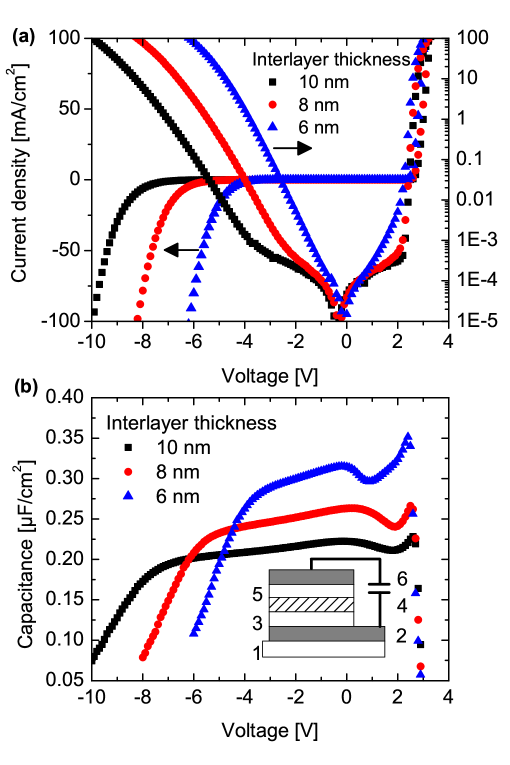
The inner structure of the organic layers follows the -concept with a highly p-type doped HTL, a highly n-type doped ETL, and an intrinsic layer in between (see Supporting Information for details). 1 displays the current-voltage (-) characteristics of such a device. In forward direction the expected diode-like behavior 16 is observed. The interlayer thickness does not affect the onset and the slope of the current rise in forward direction, which appears at 2.3 V. In contrast, there is a significant influence on the reverse current, which can be seen in the loss of the rectifying property at a certain voltage depending on the interlayer thickness. The onset of the reverse breakdown shifts in a controlled manner to higher negative voltages (from -3 V to -15 V) by increasing the interlayer thickness (see 1a): we observe a shift of the reverse breakdown voltage of approximately 1 V by each additional nanometer of IIL thickness. Current densities of more than 300 mA/cm2 in reverse direction can be achieved without limiting reversibility or reproducibility. Obviously, the large reverse voltage region is dominated by a purely exponential rise of the current, which provides a strong hint for a tunneling like mechanism. Also a flat part of the - curve can be observed in reverse direction. Since this is more pronounced for thicker interlayers it is considered to be related to a leakage currents. Hence, a larger field and a larger voltage are needed to be in the tunneling regime for thicker interlayers. The limitation of the transport layers and the injection gives rise to the flattening of the - curve for larger negative voltages.
To further understand these observations, we perform capacitance-voltage (-) measurements, allowing to study the voltage-dependent effects of charge depletion and accumulation in the IIL and allow correlating layer thicknesses to capacitance values. In our devices, the transport layers have a larger thickness and a better conductivity in comparison to the IIL which is thus the dominating -element in the stack. Capacitance frequency (-) measurements are done in order to prove independently the capacitance calculated by the assumption of one dominant -circuit (see Supporting Information). Thus, it is checked that the calculated capacitance at 0 V corresponds to the assumed interlayer thickness, which means that the IIL is still depleted even for such thin films and no diffusion of dopants occurs. The - curves shown in 1b obey the Mott-Schottky rule as long as no significant current appears (between 0 V and -4 V, see Supporting Information). In the forward voltage direction thus, a sudden capacitance drop appears independently of the IIL thickness at 2.3 V, where the geometrical capacitance dominates the - curves since the flat-band condition is reached. The small drop of capacitance for a small forward bias is related to the ETL system of cesium doped BPhen. The significant number of trap states in this material which will be filled under forward voltage conditions causes the drop in capacitance. As one can see e.g. in 3b this effect does not appear in doped RE68. However, in reverse direction, a weak decrease of the capacitance is observed as predicted by the Mott-Schottky rule. This corresponds to a charge depletion at the HTL/IIL and ETL/IIL interfaces. Besides this, a drop of the capacitance is obtained as expected from the - curves for certain reverse voltages depending on the IIL thickness caused by a significant injection into the ILL.
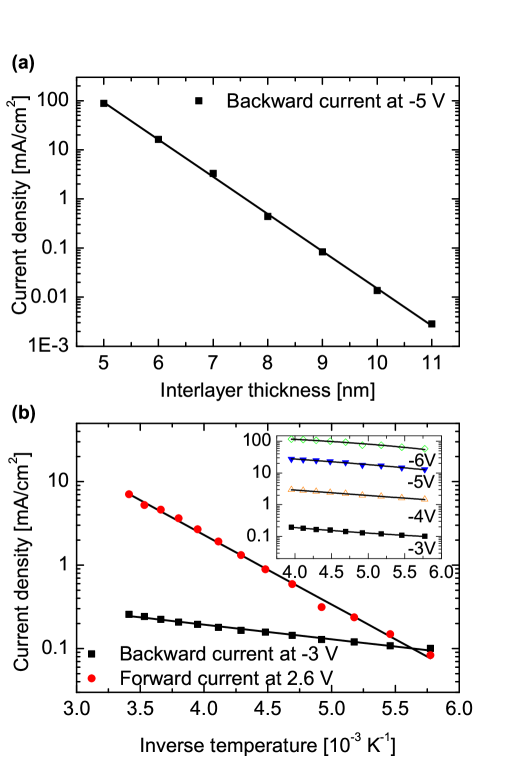
To demonstrate the control of the reverse behavior and to discuss the possible relevant charge transport mechanisms, we plot in 2 the reverse current for different temperatures and IIL thicknesses. For decreasing ILL thickness (from 11 nm to 5 nm), a purely exponential current dependence is observed (for reverse voltages larger than -3 V), with an increase of the reverse current by nearly six orders of magnitude.
A further strong evidence of tunneling is the observed temperature dependence: In addition to the exponential behavior, we find a rather weak influence of the temperature on the reverse current. In contrast to a typical activation energy of the forward current (=(17020) meV) for such a -device, 20 a surprisingly small activation energy of =(3010) meV is measured in the reverse direction, without any voltage dependence (see inset of 2b). This low reverse activation energy can be interpreted as being related to HOMO-LUMO tunneling processes which become dominant in this voltage region. The difference between this proposed mechanism and the effect described by Drechsel et al. 21 can clearly be seen in the weak interlayer thickness dependence of the backward current reported by Drechsel. This is mainly due to a change in the injection conditions for majority charge carriers at the schottky contact and not related to a tunneling of minority charge carriers as reported here. Concerning the activation energy in reverse direction it should be mentioned that since we can not neglect the influence of the transport layers to the temperature dependence the real value of activation energy remains elusive. However, even if the found temperature and interlayer dependences are a strong evidence for a tunneling mechanism a second effect, the Avalanche breakdown, could also play a role as a possible transport mechanism. Since we obtain an exponential current-voltage characteristic for different interlayer thicknesses and for a large voltage region just one kind of these two processes is supposed to be dominant. Avalanche and Zener breakdown are distinguishable by the field, which needs to be applied to be in the breakdown region. 7, 8 Thus, for a certain energy gap of the materials used for the diode Zener tunneling should appear for lower fields than Avalanche multiplication. Since we do not obtain a second process in the current-voltage curves for higher voltages the Zener effect is supposed to be the dominant mechanism.
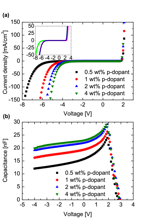
If one assumes a transport mechanism similar to inorganic Zener diodes, one can further expect a control of the reverse breakdown by the doping concentration of the transport layers. 3 shows data a for a diode of RE68 designed as a homojunction: the breakdown voltage can be shifted to higher values for lower doping concentrations as expected. The reason is a change of the effective thickness of the intrinsic layer by an additional depletion region at the HTL/IIL and the IIL/ETL interface. Although the reverse current has a reduced sensitivity to the doping concentration than to the IIL thickness, this allows a second independent approach to control the breakdown voltage. Furthermore, we also obtain no influence on the forward direction of the diode, which means that neither the series resistance of the transport layers nor the flat-band condition have been significantly changed.
- spectroscopy investigations (see 3b) once more reveal a Mott-Schottky like behavior for different doping concentrations. Obviously, there is an increase of the capacitance for a decreasing concentration of dopant molecules. Hence, if the thickness of the depletion layer is calculated from the capacitance, one obtains e.g. 8.3 nm for the 4 wt% of dopants and 11.3 nm for the 0.5 wt% of dopants (including the IIL thickness of 7 nm). This means that the depletion region thickness is the sum of the IIL and the interface depletion thickness, being sensitive to the doping concentration. We obtain a similar rule as mentioned before in case of the thickness controlled reverse current: the reverse breakdown can be shifted by 1 V or the reverse current can be increased by one order of magnitude by adding one additional nanometer to the thickness of the depletion layer (IIL plus interface depletion). This doping controlled reverse behavior can also be obtained for various concentrations of n-type dopants in ETL without any noticeable difference. Instead of NDN1 one can use cesium as a freely available n-type dopant (see Supporting Information).
Theoretical Modeling. The IIL part of the device is not expected to have an ordered crystalline structure, but rather display a high degree of static and dynamic disorder. Since the spatial arrangement of the molecular building blocks in the IIL is not known a priori, a first-principle description of the IIL electronic structure as well as of charge migration 9, 10, 11 in such a system represents a very strong challenge. Hence, to gain a first qualitative insight into the possible charge transport pathways, we have adopted a minimal model approach. Basically, the model consists of an electronic ladder with blocks describing the IIL, each block containing two energy levels whose energetic position is determined not only by the intrinsic electronic structure of a molecular building block but also by the built in field and by the applied voltage (see inset of 4). The Hamilton operator for this tight-binding model can be written as:
| (1) | |||||
The levels are denoted by (highest occupied molecular orbital, HOMO) and (lowest-unoccupied molecular orbital, LUMO) and are thus representative of the frontier orbitals of a given molecular unit. Their energetic position is assumed to be given by the linear relation: , where is the bare onsite energy of the molecular orbital (assumed to be site- independent for simplicity). The local H-L gap 3.0eV is taken from the experimental energy diagram profiles. The built-in electric field is modeled as a linear ramp with slope , which is supported by the current experiments as well as by photo-electron spectroscopy measurements in organic -diodes. 19 The second, third, and fourth summands in Eq. 1 describe different electronic couplings within the ladder: intra- strand nearest-neighbor couplings (second term) as well as nearest- and next-nearest neighbor inter-strand interactions (third and fourth terms). If not stated otherwise, we will assume for the sake of simplicity in the calculations and and , with . All electronic parameters can in principle be obtained from microscopic first-principle calculations; this goes however beyond the scope of the present minimal model approach. The last row in Eq. 1 describes the electronic structure of the (left) and (right) electrodes and the coupling between them and the ladder. The specific electronic properties of the electrodes will not appear explicitly in our treatment; they are considered only as sinks of charges and will be included in the calculations via phenomenological parameters. The electrode-ladder interaction, given by the matrix elements is in general not limited to the ladder sites nearest to the electrodes but it can have a longer range. This will qualitatively account for the fact that the real structural molecular arrangement in the active region does not in general have a linear chain topology it is expected to rather be a complex network so that interactions do not necessarily have to be confined to the electrodes’ nearest neighboring molecular blocks.
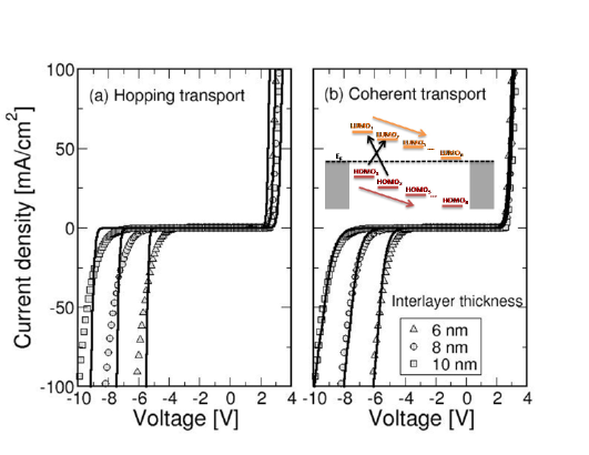
The Ansatz for allows to account qualitatively for two different physical scenarios: with increasing , the built-in field can be progressively counter-acted by the voltage-dependent term , the energy levels become increasingly aligned and the current can dramatically grow due to the reduction of tunnel barriers between the sites. For negative bias, transport is blocked up to a critical bias ; the energy scale is roughly related to the situation where the -level at a site and the -level at site become nearly resonant (additionally, at least the first site of the -strand should move above the left chemical potential in order to have a current flow). Once this happens, an exponential current onset can occur. We have used two different modeling strategies based on two possible different microscopic transport mechanisms: hopping transport (HT) and coherent tunneling (CT). HT seems to be reasonable, since it is expected that the active device region displays some degree of static and dynamic disorder which may suppress coherent tunneling pathways over long distances. We have used a reduced density matrix approach 22 (for HT) and the Landauer formalism 23 to compute the - characteristics of the model in the CT regime (see the Supporting Information for details of the calculation).
The results (scaled by an arbitrary factor) are displayed in 4 in comparison with the experiments. It is obvious that the weak (strong) thickness dependence for positive (negative) voltages can be qualitatively described within both transport regimes. Notice, however, the different number of sites needed in both regimes to account for the experimental curves, This is related to the fact that tunneling processes can still be efficient for short lengths, so that almost no zero-current gap is obtained. Only with increasing length tunneling transport is blocked at low bias.
Some basic features of the transport process can be summarized as follows: for positive voltages the onset of current takes place approximately at the critical bias where the first site of the HOMO-strand moves above the left chemical potential (which is kept fixed at while ). Under this condition, charge transport can take place. A further increase of the bias leads to an increase of the current till all the electronic levels along the ladder become aligned (the external potential cancels the built-in field ). This provides the maximum current in this model; for larger positive voltages the misalignment of the levels develops again and negative differential resistance can eventually be obtained. For negative voltages, the current is almost zero in the case of coherent tunneling, since this process is very sensitive to the presence of energy gaps along the ladder. This behavior can be lifted by allowing for long-range interactions between the electrodes and the ladder states (see Eq. 7 in the Supporting Information). On the contrary, hopping transport can also take place in the negative bias regime with only nearest-neighbor interactions.
Our results suggest that the effective microscopic transport mechanism may include both HT and CT contributions, each of them becoming dominant in different voltage regions. This may be the reason for the different slopes in the vs. plots for positive and negative voltages (2). A pure CT model cannot account for a -dependence; HT contributions can however explain it. In the HT regime, a different qualitative behavior for positive and negative voltages is expected on the basis of a simple argument: the nearest neighbor inter-site hopping rates within the ladder include (see Eq. 4 in the Supporting Information) thermal factors , whenever . For (sites on different strands), one obtains ; from here it is obvious that for the temperature dependence is mainly determined by the gap (large slope). For negative bias, can be partially compensated by the term and thus the temperature dependence may be weakened. A more accurate quantitative analysis requires a systematic experimental study of the temperature dependence, taking also the influence of the transport layers into account.
Conclusions. In this Letter, we unambiguously observe signatures of Zener tunneling in a organic molecular semiconductor: The reverse currents in organic -diodes show geometry, field and temperature dependence in excellent agreement with this tunneling effect not observed so far in such systems. The realized -Zener diodes have excellent device properties and allow important application possibilities, e.g. to reduce crosstalk in passive matrix arrays. The basic effect of valence- to conduction-level tunneling could be used in further device concepts, such as devices employing tunable resonant tunneling. Using a minimal model Hamiltonian, we can describe semi-quantitatively the measured electrical response. However, both limiting cases investigated here, incoherent hopping or coherent tunneling, can describe the observed experimental features. It therefore seems appealing to expect that the dominant charge transport mechanism may sensitively depend on the sign of the applied bias. A further point to be considered is the coupling to dynamical degrees of freedom which may induce polaron formation, so that the transport process will be rather mediated by dressed electrons or holes. We have not taken these issues in our model which is only addressing electronic degrees of freedom. Further work in this direction including detailed first-principle electronic structure calculations is thus needed.
The authors thank Novaled AG, the free state of Saxony and EU (EFRE) for financial support under project NKOE (12712) and Novaled for providing the HTL dopant NDP2 and the ETL dopant NDN1. This work was also supported by the Volkswagen Foundation through grant no. I/78-340, by the cluster of excellence of the Free State of Saxony European Center for Emerging Materials and Processes Dresden ECEMP/A2, and by WCU (World Class University) program through the Korea Science and Engineering Foundation funded by the Ministry of Education, Science and Technology (Project No. R31-2008-000-10100-0).
References
- Tang and VanSlyke 1987 Tang, C. W.; VanSlyke, S. A. Appl. Phys. Lett. 1987, 51, 913
- Burroughes et al. 1990 Burroughes, J. H.; Bradley, D. D. C.; Brown, A. R.; Marks, R. N.; Mackay, K.; Friend, R. H.; Burns, P. L.; Holmes, A. B. Nature 1990, 347, 539
- Ouyang et al. 2004 Ouyang, J.; Chu, C.; Szmanda, C. R.; Ma, L.; Yang, Y. Nature 2004, 3, 918–922
- Horowitz 1998 Horowitz, G. Adv. Mat. 1998, 10, 365–377
- Yang and Heeger 1994 Yang, Y.; Heeger, A. J. Nature 1994, 372, 344–346
- Steudel et al. 2005 Steudel, S.; K. Myny and, V. A.; Deibel, C.; de Vusser, S.; Genoe, J.; Heremans, P. Nat. Mat. 2005, 4, 597–600
- Sze and Gibbons 1966 Sze, S. M.; Gibbons, G. Appl. Phys. Lett. 1966, 8, 111
- McAfee et al. 1951 McAfee, K. B.; Ryder, E. J.; Shockley, W.; Sparks, M. Phys. Rev. 1951, 83, 650–651
- Vehoff et al. 2010 Vehoff, T.; Chung, Y. S.; Johnston, K.; Troisi, A.; Yoon, D. Y.; Andrienko, D. The Journal of Physical Chemistry C 2010, 114, 10592
- Troisi et al. 2009 Troisi, A.; Cheung, D. L.; Andrienko, D. Phys. Rev. Lett. 2009, 102, 116602
- Grozema and Siebbeles 2008 Grozema, F. C.; Siebbeles, L. D. A. International Reviews in Physical Chemistry 2008, 27, 87–138
- Ortmann et al. 2009 Ortmann, F.; Bechstedt, F.; Hannewald, K. Phys. Rev. B 2009, 79, 235206
- Scott and Bozano 2007 Scott, J. D.; Bozano, L. D. Adv. Mat. 2007, 19, 1452
- Lindner et al. 2008 Lindner, F.; Walzer, K.; Leo, K. Appl. Phys. Lett. 2008, 93, 233305
- Liang et al. 2003 Liang, G.; Cui, T.; Varahramyan, K. Micro. Eng. 2003, 65, 279–284
- Harada et al. 2005 Harada, K.; Werner, A. G.; Pfeiffer, M.; Bloom, C. J.; Elliott, C. M.; Leo, K. Phys. Rev. Lett. 2005, 94, 033601
- Walzer et al. 2007 Walzer, K.; Maennig, B.; Pfeiffer, M.; Leo, K. Chem. Rev. 2007, 107, 1233
- Blochwitz et al. 2001 Blochwitz, J.; Fritz, T.; Pfeiffer, M.; Leo, K.; Alloway, D.; Lee, P.; Armstrong, N. Org. Electron. 2001, 2, 97
- Olthof et al. 2009 Olthof, S.; Meerheim, R.; Schober, M.; Leo, K. Phys. Rev. B 2009, 79, 245308
- Maennig et al. 2001 Maennig, B.; Pfeiffer, M.; Nollau, A.; Zhou, X.; Leo, K. Phys. Rev. B 2001, 64, 195208
- Drechsel et al. 2002 Drechsel, J.; Pfeiffer, M.; Zhou, X.; Nollau, A.; Leo, K. Syn. Met. 2002, 127, 201–205
- Blum 1996 Blum, K. Plenum Press 1996
- Datta 1995 Datta, S. Cambridge University Press, Cambridge 1995
The Supporting Information Section includes preparation methods, additional -, -, - and Mott-Schottky-curves for the free available materials. Furthermore we present a more detailed description of the microscopic model applied to describe the charge transport characteristics in the organic Zener diode.