Broadband enhancement of light harvesting in luminescent solar concentrator
Abstract
Luminescent solar concentrators (LSCs) are large-area devices that may absorb incident sunlight, then emit luminescence photons with high quantum efficiency which finally be collected by a small photovoltaic (PV) system. The light-harvesting area of the PV system is much smaller than that of the LSC system, potentially reducing the cost of solar cells. Here, we present a theoretical description of the luminescent process in nanoscale LSCs where the conventional ray-optics model is no longer applicable. We demonstrate that a slot waveguide consisting of a nanometer-sized low-index slot region sandwiched by two high-index regions provides a broadband enhancement of light harvesting by the luminescent centers in the slot region. This is because the slot waveguide can (1) greatly enhance the spontaneous emission due to the Purcell effect, (2) dramatically increase the effective absorption length of luminescent centers, and (3) strongly improve the fluorescence quantum yield of luminescent centers. It is found that about solar photons can be re-emitted even for a low fluorescent quantum yield of , and re-emitted photons can be coupled to the slot-waveguide. This LSC is potential to construct a tandem structure which can absorb nearly full-spectrum solar photons, and also may be of special interest for building integrated nano-solar-cell applications.
In the past few years, many approaches involving nanostructures or nanostructured materials have been proposed to reduce cost and improve efficiency in both experiment nano3 ; nano4 ; nano8 ; nano12 and theory t2 ; t5 ; t6 . On the other hand, concentrators with large-area optical components to collect direct sunlight and transfer the energy to small, high-efficiency photovoltaic (PV) cells have been suggested as a simple approach to lower the cost per peak Watt of solar cell systems for many decades jason . To overcome the excess heat problem, chromatic aberrations and expensive maintaining in these imagining concentrators, luminescent solar concentrators (LSCs) represent an alternative approach to lower the costs of solar cell systems batchelder ; weber ; AP1977 ; michael ; IEEE . LSCs generally consist of low-cost transparent sheets doped with luminescent species, such as dye molecules and quantum dots. Incident sunlight is highly absorbed by the luminescent centers and luminescence is emitted with high fluorescence quantum yield (FQY, defined as the ratio of the number of photons emitted to the number of photons absorbed), so that the emitted photon is trapped in the sheet by total internal reflection and travels to the edges where it can be collected by solar cells. The active material layer can be much thinner than the intrinsic absorption length of the material, thus dramatically reducing the amount of the solar cell material.
One of the key parameters of LSCs is the coupling efficiency which describes the ratio of luminescent photons coupled to waveguide modes for ultimate collection by PV systems on the waveguide edge. To model these LSCs devices, thermodynamical and computational ray tracing approaches have been introduced, and both approaches represent a broad-scale, macroscopic model michael ; Chatten ; Earp ; Carrascosa ; Rau . For example, conventional LSCs have a thickness much larger than the wavelength, so that the ray-optics model can be applied to estimate the collection efficiency of luminescence by the solar cell. However, with LSCs devices moving to the nanoscale, the ray-optics picture and some basic assumptions are no longer strictly applicable. In this paper, we propose a nanometer-sized slot waveguide as the main structure of LSCs, and theoretically study the enhancement of spontaneous emission (described by the factor ) of luminescent centers in this slot waveguide based on the Fermi-golden rule. Remarkably, this great enhancement of spontaneous emission predicts not only an increased absorption length of luminescent centers but also a very large waveguide coupling efficiency . We demonstrate that such a slot waveguide LSC provides a broadband enhancement of light harvesting. It is found that about solar photons can be re-emitted even for a low initial FQY of , and re-emitted luminescent photons can be coupled into the slot waveguide modes for ultimate collecting by the solar cell located on the waveguide edge. This LSCs may be of special interest for building integrated solar cell applications.
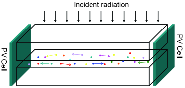
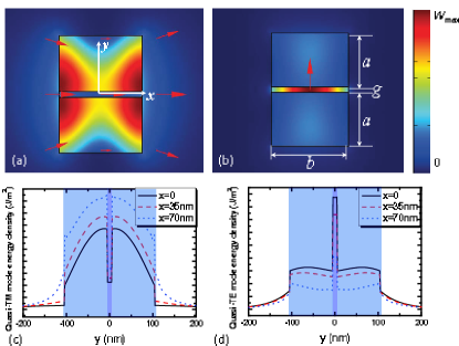
The basic structure of the proposed design is shown in Figure 1 and the cross-sectional geometry is depicted in Figure 2(b). The slot waveguide consists of a nanometer-sized low-index slot region (with the permittivity , here is assumed ) sandwiched by two high-index transparent layers (with the permittivity , here is assumed ), and the PV systems are on the edge of the slot waveguide. In this work, high-index polymer or glass layers are desirable to indeed reduce the cost, but it requires future studies. Active medium such as dye molecules and quantum dots are doped in the slot region. The active medium absorbs the incident sunlight and re-emits the luminescence with a red-shifted wavelength. Different from the conventional waveguides, slot waveguide is able to guide and strongly confine light in a nanoscale low-index material. Quantitatively, the mode area of the slot waveguide can be reduced to at least of the conventional one. For instance, the effective mode areas are about and for waveguides in Figure 2 with and without the slot, respectively. The basic principle of slot waveguide is based on the discontinuity of the electric field at a normal boundary between two materials OL2004 . When the electromagnetic wave propagates along the waveguide direction, the major component of the electric field of the quasi-transverse electric (TE) mode undergoes a discontinuity at the slot interfaces. According to the boundary condition of Maxwell’s equations, the amplitude of the electric field in the low-index slot is much larger than that in the high-index waveguides, and the ratio between them is . With a full-vectorial finite element method (FEM), we can simulate the modes in the structure. As shown in Figure 2, the electric field of the quasi-TE mode is strongly concentrated in the slot region and it is normal to the interface, while the electric field of the quasi-transverse-magnetic (TM) mode distributes over the whole cross-sectional area and it is parallel to the interface. This unique characteristic makes the slot waveguide attractive for numerous applications, for instance, highly sensitive biosensors OL2007 and waveguide-based light source OE2009 . In this paper, also due to the large electric field intensity of the slot waveguide mode, the luminescent photons are expected to couple to the propagating slot mode, and finally be collected by the smaller high-efficiency PV systems. Due to the concentration effect at the LSCs edges, the amount of the solar cell material reduces dramatically, and the cost of solar cell may decrease greatly with the help of the slot waveguide LSC.
To analyze this LSC system, we note that the conventional ray-optics model is not applicable because the thickness of the slot region is nanometer-sized. Thus, we derive a simple analytical formula from the Fermi-golden rule to obtain the spontaneous emission enhancement and the waveguide coupling ratio . In the weak-coupling regime, the spontaneous emission rate of a dipole can be calculated from
| (1) |
where denotes the coupling strength between the dipole and the electromagnetic field at the dipole position . represents the density of states. If we assume that the dipole is oriented parallel to the electric field, the coupling strength is then given by
| (2) |
with
| (3) |
Here designates the normalized electromagnetic energy density distribution; defines the effective mode area as
which plays the role analogous to the mode volume in cavity QED; is an arbitrary quantization length which can be canceled later. For a slot waveguide with a sufficiently small cross-sectional area, it only supports a single quasi-TE and a single quasi-TM mode. As mentioned before, the TE mode has the maximum electric field in the slot region. Thus, assuming a one-dimensional density of states, the density of states can be expressed as
| (4) |
where is the group velocity of the slot waveguide mode with a group index . Here, is the light velocity in vacuum. Combining Equations (1)-(4), we can obtain the spontaneous emission rate of the dipole in the slot waveguide
| (5) |
With the spontaneous emission rate into free space , the emission enhancement also known as Purcell effect, is thus expressed as
| (6) |
Clearly, if the effective mode area of the slot waveguide mode is squeezed significantly below , the light-matter interaction can be dramatically enhanced, thus leading to an enhanced . In addition, the group velocity in the slot waveguiding mode is reduced, which can furthermore increase the local density of states and also contribute to the increase of . Once the emission enhancement is given, the waveguide coupling efficiency describing the ratio of the emission coupled to the slot waveguiding mode, can be calculated as
| (7) |
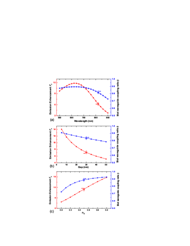
Equations (6) and (7) represent the main physical parameters of the proposed LSC. To numerically evaluate the emission enhancement and the waveguide coupling efficiency, we still resort to the FEM simulation, as it can provide not only the mode distribution (, ) but also the group velocity for a given geometry and working wavelength. Figure 3(a) shows the calculated and as a function of free-space wavelength when a dipole is placed in the center of the cross-section of the slot waveguide. We find two points. (i) first increases and then decreases with the emission wavelength from to nm. This phenomenon is because that the effective mode area first decreases and then increases. For the short wavelength, most energy distributes in the high-index layers, and the field enhancement effect in the slot becomes weaker. As a result, the effective mode area increases. For the long wavelength, the small size of the slot waveguide cannot support the guiding mode well. Therefore, more and more energy diffuses outside for longer wavelength, and the effective mode area strongly expands. (ii) exceeds over a broad wavelength range ( nm). For longer wavelengths, a larger-sized slot waveguide can be employed to reach the maximum , which will be discussed in the following. This strong enhancement of the spontaneous emission takes advantage of nonresonance (large bandwidth), which benefits from the subwavelength mode area (as small as ) and the reduced group velocity (with the group index ) provided by the slot waveguide. Remarkably, this broadband enhancement character overcomes the narrow bandwidth limit of a microresonator-based emission enhancement. As a result, most of the spontaneous emission can efficiently couple to the slot waveguide mode, and exceed over a broad wavelength range ( nm).
The enhancement of spontaneous emission also depends on the geometry of the slot waveguide, for example, the slot width. Figure 3(b) shows the calculated enhancement factor as a function of the slot width . The factor increases monotonically with the slot width reducing. For example, increases from to when decreases from to nm. The underlying physics is that both the effective mode area and the group velocity are strongly reduced by decreasing the slot width. For instance, and are and at nm, and at nm. Thus, in this slot width range, the waveguide coupling efficiency changes from to .
As mentioned above, we use as the default . However, for a different , and can experience a significant change. From Figure 3(c) we can see that with a larger , both and improve, which is because high-index-contrast interfaces can bring out a better enhancement and confinement of light OL2004 . Therefore, materials with both high transparency and refractive index are strongly preferred in our work.
In the analysis above, we have assumed that the dipole is oriented parallel to the electric field of the quasi-TE mode. In an actual case, the orientation of a dipole may be isotropically distributed over any direction. In general, the quasi-TE mode has a much stronger electric field concentration in the slot region than the quasi-TM mode. As a result, the dipole oscillating in the direction (coupled to the quasi-TE mode) exhibits a much larger emission enhancement than the dipole oscillating in the direction (coupled to the quasi-TM mode). In addition, the spontaneous emission enhancement of the dipole oscillating in the direction is even smaller because both the modes are quasi-transverse. The isotropically averaged emission enhancement factor can be calculated by
| (8) |
where denotes the spontaneous emission enhancement when the dipole oscillates in the direction. With , the isotropically averaged waveguide coupling efficiency is thus obtained as
| (9) |
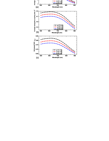
Figures 4(a) and 4(b) show and , respectively, depending on the emission wavelength for three different slot widths nm. From Figure 4(a), on one hand, due to enhanced dipole-field coupling, increases as the slot width decreases. On the other hand, still keeps high over the whole calculation range from to nm. Thus, even if dipoles oscillate in random directions, most emission of the dipoles will couple into the waveguide modes. For instance, as demonstrated in Figure 4(b), the averaged waveguide coupling efficiency is high above over a broad wavelength range in the case of nm.
It should also be noted that only spontaneous emission rate is speeded up by the concentrated slot mode, while the intrinsic nonradiative decay path related to the initial FQY keeps unchanged, leading to an enhanced FQY Purcell . The discussion above has assumed a unit initial FQY (). For a finite FQY, however, we find that the spontaneous emission enhancement can actually enhance the FQY. In the slot waveguide, the modulated (enhanced) FQY describing the ratio of the radiation, can be calculated by
| (10) |
As demonstrated in Figure 4(c), for an initial , the modified FQY exceeds over a broad wavelength range in the case of nm.
We turn to analyze the total photon conversion efficiency of this LSC. Besides the isotropically averaged waveguide coupling efficiency and the modified FQY , the total efficiency should also include the solar photon absorption efficiency by the active medium, the transportation efficiency from emitters to the PV systems. Thus, we have
| (11) |
In the following we will explain how the slot waveguides play significant roles in obtaining a high . First, depends on the intrinsic property of the active medium, such as the absorption cross-section and the absorption spectrum. Interestingly, the absorption ability of single emitters is expected to be improved due to the enhanced emission with a high in the slot waveguide. A higher corresponds to a faster spontaneous emission of the active medium molecules, which implies the stimulated molecules can go back to their ground state faster and the round time of the absorption-emission process is significantly shortened Purcell . In other words, the absorption length of the slot region is efficiently increased. Second, in Figure 4, both and are improved over a broad wavelength range, which can be further improved by aligning the dipoles of luminescent centers parallel to the electric field of quasi-TE modes Rowan ; 2009AFM . Third, the luminescent photons should be transported to the LSCs edges where the PV systems can absorb these photons and convert them to photoelectrons. In this process, the photon transportation efficiency can be high because the slot provides good propagating modes along direction. Nevertheless, may be degraded by the re-absorption phenomenon of the active medium. Potentially, the re-absorption can be suppressed by choosing luminescent centers whose absorption and emission spectra have a small overlap due to a large Stokes shift STOKES , or using luminophores with unitary FQY which effectively close the nonradiative decay channel.
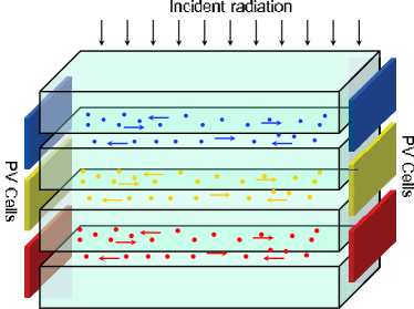
Finally, it should be noticed that slot waveguides possess an optimized geometrical size for a specific wavelength band. For instance, if the thickness of high-index layers is too large, more energy will distribute in the high-index layers and less in the slot waveguide, so the Purcell effect of this structure will be dramatically weakened. As an example, if we increase the size to , for nm wavelength in Figure 3(a), decreases from to , and from to . Nevertheless, an expanded geometry is required to support propagating modes well in the slot waveguide for long wavelengths. To obtain the highest power efficiencies, on one hand, the absorption band can be broadened by mixing dyes and quantum dots with different sizes. On the other hand, it is also potential to construct tandem LSCs which can absorb more solar photons in a broad band. Incident solar photons are first absorbed by a LSC employing a short-wavelength active medium, such as a specific dye. Photons with longer wavelengths are transmitted through the first LSC and then absorbed by the second LSC employing a long-wavelength active medium and an expanded geometry , as shown in Figure 5. To fabricate such a LSC structure, a nanoimprinting technique can be utilized which can reach large areas up to several inches wide ACSnano .
In summary, we present a theoretical description of nanoscale LSCs where the conventional ray-optics model is no longer applicable. Based on the Fermi-golden rule, we evaluate the spontaneous emission enhancement and the waveguide coupling efficiency in a slot waveguide consisting of a nanometer-sized low-index slot region sandwiched by two high-index regions. It is found that the slot waveguide provides a broadband enhancement of light harvesting by the luminescence centers in the slot region. In spite of a low initial FQY , approximately solar photons can re-emit as luminescent photons, and more than luminescence can be coupled into the waveguide modes for ultimate absorption by the solar cell located on the waveguide edge. This LSCs scheme holds a great potential to
construct a tandem structure which can absorb nearly full-spectrum solar photons, and is of special interest for building integrated nano-solar-cell applications.
Acknowledgment. The authors acknowledge financial support from the National Natural Science Foundation of China under Grant No. 10821062 and 11004003, the National Basic Research Program of China under Grant Nos. 2007CB307001 and 2009CB930504. Yun-Feng Xiao was also supported by the Research Fund for the Doctoral Program of Higher Education (No.20090001120004) and the Scientific Research Foundation for the Returned Overseas Chinese Scholars.
References
- (1) W. U. Huynh, J. J. Dittmer, A. P. Alivisatos, ”Hybrid nanorod-polymer solar cells,” Science, vol. 295, pp. 2425-2427, 2002.
- (2) M. Law, L. E. Greene, J. C. Johnson, R. Saykally, P. Yang, ”Nanowire dye-sensitized solar cells,” Nature Material, vol. 4, pp. 455-459, 2005.
- (3) D. H. Ko, J. R. Tumbleston, L. Zhang, S. Williams, J. M. DeSimone, R. Lopez, E. T. Samulski, ”Photonic Crystal Geometry for Organic Solar Cells,” Nano Lett., vol. 9, pp. 2742-2746, 2009.
- (4) J. G. Mutitu et al., ”Thin film solar cell design based on photonic crystal and diffractive grating structures,” Opt. Express, vol. 16, pp. 15238-15248, 2008.
- (5) A. Aubry et al., ”Plasmonic light-harvesting devices over the whole visible spectrum,” Nano Lett., vol. 10, pp. 2574-2579, 2010.
- (6) L. Y. Cao et al., ”Semiconductor Nanowire Optical Antenna Solar Absorbers,” Nano Lett., vol. 10, pp. 439-445, 2010.
- (7) W. Wang, S. Wu, K. Reinhardt, Y. Lu, S. Chen, ”Broadband light absorption enhancement in thin-film silicon solar cells,” Nano Lett., vol. 10, pp. 2012-2018, 2010.
- (8) J. H. Karp, E. J. Tremblay, J. E. Ford, ”Planar micro-optic solar concentrator,” Opt. Express, vol. 18, pp. 1122-1133, 2010.
- (9) W. H. Weber, J. Lambe, ”Luminescent greenhouse collector for solar radiation,” Appl. Opt., vol. 15, pp. 2299-2300, 1976.
- (10) J. S. Batchelder, A. H. Zewail, T. Cole, ”Luminescent solar concentrators 2: Experimental and theoretical analysis of their possible efficiencies,” Appl. Opt., vol. 20, pp. 3733-3754, 1981.
- (11) A. Goetzberger, W. Greubel, ”Solar energy conversion with fluorescent collectors,” Appl. Phys., vol. 14, pp. 123-139, 1977.
- (12) M. J. Currie, J. K. Mapel, T. D. Heidel, S. Goffri, M. A. Baldo, ”High-Efficiency Organic Solar Concentrators for Photovoltaics,” Science, vol. 321, pp. 226-228, 2008.
- (13) B. C. Rowan, L. R. Wilson, B. S. Richards, ”Advanced Material Concepts for Luminescent Solar Concentrators,” IEEE J. Selected Topics in Quantum Electron., vol. 14, pp. 1312-1322, 2008.
- (14) A. J. Chatten, K. W. J. Barnham, B. F. Buxton, N. J. Ekins-Daukes, M. A. Malik, ”Quantum Dot Solar Concentrators,” Semiconductors, vol. 38, pp. 609-617, 2004.
- (15) A. A. Earp, G. B. Smith, P. D. Swift, J. Franklin, ”Maximising the light output of a Luminescent Solar Concentrator,” Sol. Energy, vol. 76, pp. 655-667, 2004.
- (16) M. Carrascosa, S. Unamuno, F. Agullo-Lopez, ”Monte Carlo simulation of the performance of PMMA luminescent solar collectors,” Appl. Opt., vol. 22, pp. 3236-3241, 1983.
- (17) U. Rau, F. Einsele, G. C. Glaeser, ”Efficiency limits of photovoltaic fluorescent collectors,” Appl. Phys. Lett., vol. 87, pp. 171101, 2003.
- (18) V. R. Almeida, Q. F. Xu, C. A. Barrios, M. Lipson, ”Guiding and confining light in void nanostructure,” Opt. Lett., vol. 29, pp. 1209-1211, 2004.
- (19) C. A. Barrios et al., ”Slot-waveguide biochemical sensor,” Opt. Lett., vol. 32, pp. 3080-3082, 2007.
- (20) Y. C. Jun. R. M. Briggs, H. A. Atwater, M. L. Brongersma, ”Broadband enhancement of light emission in silicon slot waveguides,” Opt. Express, vol. 17, pp. 7479-7490, 2009.
- (21) P. Goy, J. M. Raimond, M. Gross, S. Haroche, ”Obervation of cavity-enhanced single-atom spontaneous emission,” Phys. Rev. Lett., vol 50, no. 24, pp. 1903-1906, 1983.
- (22) R. W. MacQueen, Y. Y. Cheng, R. G. C. R. Clady, T. W. Schmidt, ”Towards an aligned luminophore solar concentrator,” Opt. Express, vol. 18, pp. A161-A166, 2010.
- (23) Paul P. C. Verbunt, A. Kaiser, K. Hermans, C. W. M. Bastiaansen, D. J. Broer, M. G. Debije, ”Controlling Light Emission in Luminescent Solar Concentrators Through Use of Dye Molecules Aligned in a Planar Manner by Liquid Crystals,” Adv. Funct. Mater., vol. 19, pp. 2714-2719, 2009.
- (24) L. R. Wilson, B. C. Rowan, N. Robertson, O. Moudam, A. C. Jones, B. S. Richards, ”Characterization and reduction of reabsorption losses in luminescent solar concentrators,” Appl. Optics, vol. 49, pp. 1651-1661, 2010.
- (25) S. Ahn, L. Guo, ”Large-Area Roll-to-Roll and Roll-to-Plate Nanoimprint Lithography: A Step toward High-Throughput Application of Continuous Nanoimprinting,” ACS Nano, vol. 3, pp. 2304-2310, 2009.