Valley-Orbit Photocurrents in (111)-oriented Si-MOSFETs
Abstract
We demonstrate the injection of pure valley-orbit currents in multi-valley semiconductors and present the theory of this effect. We studied photo-induced transport in -doped (111)-oriented silicon metal-oxide-semiconductor field effect transistors at room temperature. By shining circularly polarized light on exact oriented structures with six equivalent valleys, non-zero electron fluxes within each valley are generated, which compensate each other and do not yield a net electric current. By disturbing the balance between the valley fluxes, in this work by applying linearly polarized radiation as well as by introducing a nonequivalence of the valleys by disorientation, we approve that the pure valley currents can be converted into a measurable electric current.
pacs:
78.40.Fy, 72.40.+w, 73.40.Qv, 78.20.-eFree carriers in solids can carry both positive and negative electric charge, which builds the basis for bipolar electronics. In addition, they possess degrees of freedom related to spin or valley degeneracy, the latter being relevant in multi-valley semiconductors. The degeneracies enable one to engineer various distributions of carriers in the momentum, spin, and valley spaces. A controllable way of occupying a particular spin state or filling a particular valley is a key ingredient, respectively, for spintronics spintronics or valleytronics TarIvch05 ; beenakker1 aimed at the development of novel solid-state devices. The candidates appropriate for the realization of valleytronics concepts include multi-valley semiconductors such as silicon TarIvch05 ; mcfarland , graphene beenakker1 ; garsia ; Moskalenko , and carbon nanotubes TarIvch05 . A remarkable selective population of the electron states is achieved by optical pumping with polarized light: circularly for spin polarization spin_physics and linearly polarized for “valley polarization” sokolov . Besides the selective valley population, the radiation can also cause a particle flux within each valley, whose direction and magnitude depend on the valley number . In general, the total electric current is non-zero, measurable by conventional electric methods. However, for special geometries and light polarizations, the partial fluxes do exist but the total electric current vanishes. This is the pure valley current proposed in Ref. TarIvch05 and implying the device’s potential use of the valley index in analogy to the pure spin currents in spintronics and topological electronics sipe1 ; naturephys ; sipe2 ; TarIvch08 ; Kane ; Koenig .
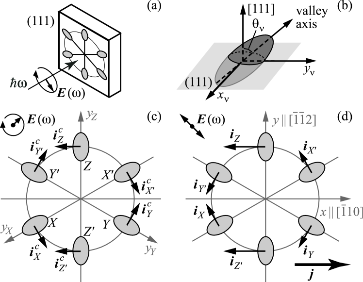
Here, we report on the vivid evidence of the existence of pure valley-orbit currents and demonstrate that the individual control of electron fluxes in valleys can be achieved by the excitation of (111)-oriented Si-metal-oxide-semiconductor (Si-MOS) structures with polarized light. Such two-dimensional systems contain six equivalent electron valleys mcfarland ; Si111 , Fig. 1, and possess the overall point-group symmetry C3v, i.e., they are invariant with respect to the rotation by an angle of . The irradiation of (111)-oriented Si-MOS structures leads to an emergence of the fluxes in all six valleys, Fig. 1(a). The generation of the fluxes is microscopically caused by the low symmetry of individual valleys, Fig. 1(b), and stems from asymmetric electron photoexcitation. This mechanism is similar to those considered in Refs. TarIvch05 ; Magarill89 ; JPCM , but out of scope of this Letter and will be described elsewhere. Instead, we focus on the distribution of the fluxes over the valleys forming the pure orbital currents or, under certain conditions, an electric current. The symmetry analysis shows that circularly polarized light normally incident upon the sample induces helicity-sensitive intravalley fluxes in the directions perpendicular to the principal valley axes resulting in a zero net photocurrent, see Fig. 1(c). On the other hand, the theory allows the generation of a total electric current by normally incident and linearly polarized radiation, Fig. 1(d). Thus, a first experimental evidence of valley currents in (111) Si-MOS structures is the lack of a net photocurrent for circularly polarized light and its observation for linear polarization. A further confirmation is the appearance of a photocurrent in samples with broken equivalence of valleys, e.g., in structures with the surface normal slightly tilted from the [111] axis.

To verify the theoretical predictions, we have experimentally studied photocurrents in MOS field-effect transistors (MOSFETs) fabricated on exact and miscut (111) silicon surfaces. The studied Si samples with the surface precisely oriented along the (111) plane contain two transistors, see inset of Fig. 2(a), each prepared with a channel length of mm, a width of mm and the channel directions parallel either to or . The channels are covered by nm thick SiO2 layers and semitransparent polycrystalline Si gates. The variation of the gate voltage from to V changes the carrier density from to cm-2. As a reference sample we also fabricated MOSFETs on exact (001) Si surfaces with similar characteristics.
Another set of MOSFETs is fabricated on Si surfaces with the normal rotated from the orientation around the axis by an angle of . The point-group symmetry of this system is Cs consisting of the identity element and the mirror rotation plane (). Two transistors with the same size are prepared on the miscut substrate with the channels oriented either along or along the inclination axis (see inset in Fig. 3). They have nm thick SiO2 layers and semitransparent polycrystalline Si gates. Variation in from to V changes from to cm-2.
All kinds of MOSFETs used in the experiment exhibit room-temperature electron mobilities in the channel between and cm2/Vs. The orientation of the Si surfaces has been proved applying an X-ray diffractometer. The accuracy of the orientation is better than .
For optical excitation we use the emission of an optically pumped terahertz (THz) molecular gas laser GanichevPrettl . The radiation with a pulse length of 100 ns and a peak power 10 kW is obtained at the wavelengths 90, 148, 280, 385 and 496 m corresponding to photon energies between and meV.
The experimental geometries are illustrated in the insets of Figs. 2 and 3. All experiments are performed at normal incidence of radiation and room temperature. In this setup, the THz radiation causes indirect Drude-like optical transitions in the Si-MOSFETs. Various polarization states of the radiation are achieved by transmitting the laser beam, which is initially linearly polarized along the (or ) axis, through /2 or /4 crystal quartz plates. By applying the plates, we vary the azimuth angle between the polarization plane of the radiation incident upon the sample and the (or ) axis, see the inset of Fig. 2(a). By applying /4 plates we transfer linearly to elliptically polarized radiation. In this case, the polarization state is determined by the angle between the (or ) axis and the optical axis of the plate. The Stokes parameters , and the degree of circular polarization , defined by , depend on the angles and as
| (1) |
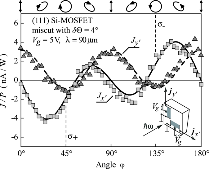
Here, is the polarization unit vector and is the photon wave vector directed along . The incident polarization states are sketched for characteristic angles on top of Fig. 3. The photocurrents are measured between source and drain contacts of the unbiased transistors via the voltage drop across a 50 load resistor.
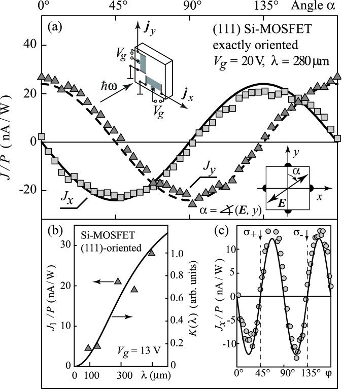
Irradiating the exact (111) Si-MOSFETs with linearly polarized THz radiation at normal incidence generates photocurrent signals with a temporal shape reproducing the laser pulse. The dependence on the azimuth angle is shown in Fig. 2(a), the data are well fitted by
| (2) |
with the same prefactor nA/W, in agreement with the theoretical expectation for the point group C3v. It has been checked that, in the reference MOSFETs prepared on the exact (001) Si surface, normal-incidence photocurrents are absent for any polarization of radiation JPCM . Triangles in Fig. 2(b) show that, as expected for the free-carrier absorption, the signal rises with increasing the wavelength following the Drude formula of high-frequency conductivity GaN2008 ; Tarasenko10 .

The variation of the photocurrent with the angle presented in Fig. 2(c) clearly demonstrates that the current vanishes for circularly polarized photoexcitation, and , realized at and . The best fit of the dependencies and (not shown) contains no contributions from and reduces to
| (3) |
with the same coefficient as in Eq. (2).
The symmetry considerations for the miscut (111) Si transistors with the Cs point group lead to the following phenomenological equations for the in-plane photocurrent components as a function of the angle
| (4) |
Figure 3 shows the effect of a miscut angle . The curves in the figure are well fitted by Eqs. (4) with the values of coefficients (in nA/W): , , , and . As compared with the exact (111) Si sample, the inclination leads to three distinctive features: (i) a current along the axis proportional to the radiation helicity is generated under normal incidence, (ii) the current component acquires a polarization-independent contribution, and (iii) the absolute values of the coefficients describing the currents induced by linearly polarized light become different.

Now we show that the observed dependencies (2)-(4) are readily obtained by summing up the photocurrents induced in individual valleys. Each valley ( and , see Fig. 1) has only one non-trivial symmetry element, the reflection , described by the point group . Here, we use the following in-plane frame: the axis is perpendicular to the plane containing the principal valley axis and the channel normal , and the axis lies in this plane. Particularly, for , the axes and coincide with and , respectively. The current density emerging in the valley is phenomenologically given by
| (5) | |||||
where is the light intensity, , , , and are polarization-independent coefficients, is the angle between the normal and the principal axis of the valley , and are the projections of the polarization vector on the and axes, respectively.
The total electric current is a sum of the single-valley contributions . In fact, the contributions due to the valleys (or and ) coincide so that the total photocurrent simplifies to
| (6) |
By projecting all the partial vectors on the transistor axes and (or and ) we obtain
| (7) | |||
where is the angle between the axes and .
In the exact (111) Si-MOS structure, all valleys are equivalent, with , and the in-plane angles are given by , . Therefore, we derive
| (8) | |||
where and . Equation (8) exactly reproduces the experimentally observed polarization dependencies (2)-(3) with the fitting parameter given by . Thus, we conclude that, while both circularly polarized and unpolarized radiation give rise to an electric currents in all valleys, the total photocurrent can only be excited by linearly polarized light.
To describe the photocurrent in miscut structures, we introduce the polar angles and of the normal in the Cartesian system [100], [010], [001]. If the channel normal is close to , then the angles and are close to and , respectively. By expanding , in powers of and one can derive the expression for the photocurrent in miscut structures. In the approximation linear in and , the total helicity-dependent current reduces to
| (9) |
where , , and is the unit vector along the crystallographic axis . While deriving Eq. (9) we took into account that (i) for a fixed value of the total electron density, the electron chemical potential is independent of and (ii) the angles are expressed in terms of , by and , and (iii) the components and are given by and , respectively. Equation (9) shows that the helicity-dependent photocurrent excited by normally incident radiation appears only in miscut structures and in the direction perpendicular to the inclination axis. This is the behavior that is observed in all Si-MOSFETs studied in experiment, see Figs. 2(c) and 3. It follows from the experimentally measured value of the ratio and from Eq. (9) that the ratio and amounts 5. An estimation based on the microscopic theory PRBSi ; Tarasenko10 of orbital mechanisms of dc currents driven by ac electric fields gives for the latter ratio a value of unity. This mismatch needs a further analysis.
The valley currents with zero net charge transfer can be classified according to their behavior under the symmetry operations. In (111)-oriented Si-MOS structures of the point group, the pure valley currents can belong to the irreducible representations , and . The scalar representation describes the pure valley current ; this current is excited by normally incident unpolarized radiation. The pseudoscalar representation describes the valley current , which changes its sign upon reflection in any of the three mirror planes of the point group . The contribution is induced by circularly polarized radiation, see Fig. 1(c), and reverses its sign upon inversion of the photon helicity. Finally, the two-dimensional vector representation describes the valley current with the components and . The polarization dependence of the pure valley current excited by normally incident radiation is given by Eq. (8) where is replaced by .
In conventional electric measurements, the pure valley currents are hidden and special methods are needed to reveal them. A possible experiment to observe is the generation of the second harmonic. Indeed, under normal incidence of the probe light, the dielectric polarization at the second harmonic frequency is given by
where is the probe electric-field amplitude, the second-order susceptibility of the equilibrium system and the third-order susceptibility, the second order in and the first in . Note that the effect of the gate voltage on the generation of the second harmonic has been previously observed in (001) Si-MOSFETs Second . Another possibility is the orbital Kerr or Faraday rotation of the probe beam caused by the pure orbit-valley current with the rotation angle , similar to spin Kerr or Faraday effect.
Support from DFG (SPP1285), Linkage Grant of IB of BMBF at DLR, RFBR, Russian Ministry of Education and Sciences, and “Dynasty” Foundation ICFPM is gratefully acknowledged.
References
- (1) I. Žutić et al., Rev. Mod. Phys. 76, 323 (2004).
- (2) S. A. Tarasenko and E. L. Ivchenko, Pis’ma Zh. Eksp. Teor. Fiz. 81, 292 [JETP Lett. 81, 231] (2005).
- (3) A. Rycerz et al., Nature Phys. 3, 172 (2007).
- (4) R. N. McFarland et al., Phys. Rev. B 80, 161310 (2009).
- (5) J. L. Garcia-Pomar et al., Phys. Rev. Lett. 100, 236801 (2008).
- (6) A. S. Moskalenko and J. Berakdar, Phys. Rev. B 80, 193407 (2009)
- (7) M. I. Dyakonov (ed.), Spin Physics in Semiconductors (Springer, 2008).
- (8) A. A. Kaplyanskii et al., Solid State Commun. 20, 27 (1976).
- (9) R. D. R. Bhat et al., Phys. Rev. Lett. 94, 96603 (2005).
- (10) S. D. Ganichev et al., Nature Phys. 2, 609 (2006).
- (11) H. Zhao et al., Phys. Rev. B 72, 201302 (2005).
- (12) S. A. Tarasenko and E. L. Ivchenko, Semicond. Sci. Technol. 23, 114007 (2008).
- (13) C. L. Kane and E. J. Mele, Phys. Rev. Lett. 95, 146802 (2005).
- (14) M. König et al., Science 318, 766 (2007).
- (15) T. Cole and B. D. McCombe, Phys. Rev. B 29, 3180 (1984).
- (16) L. I. Magarill and M. V. Entin, Fiz. Tverd. Tela 31(8), 37 (1989) [Sov. Phys. Solid State 31, 1299 (1989)].
- (17) J. Karch et al., J. Phys.: Condens. Matter 22, 355307 (2010).
- (18) S. D. Ganichev and W. Prettl, Intense Terahertz Excitation of Semiconductors (Oxford Univ. Press, 2006).
- (19) W. Weber et al., Phys. Rev. B 77, 245304 (2008).
- (20) S. A. Tarasenko, pre-print arXiv:1009.0681 (2010).
- (21) P. Olbrich et al., Phys. Rev. B 79, 121302 (2009).
- (22) J. Fang and G. P. Li, Appl. Phys. Lett. 75, 3506 (1999).