Thermoelectric transport of perfectly conducting channels in two- and three-dimensional topological insulators
Abstract
Topological insulators have gapless edge/surface states with novel transport properties. Among these, there are two classes of perfectly conducting channels which are free from backscattering: the edge states of two-dimensional topological insulators and the one-dimensional states localized on dislocations of certain three-dimensional topological insulators. We show how these novel states affect thermoelectric properties of the systems and discuss possibilities to improve the thermoelectric figure of merit using these materials with perfectly conducting channels.
1 Introduction
Topological insulators (TI) [1, 2, 3, 4, 5] have attracted a lot of attention in the recent years. In these materials the excitations in the bulk are gapped just like in the normal insulators, but due to specific topological properties of the band structure these insulators possess gapless modes at the edges (on the surface). These modes are topologically protected and are stable against any perturbations that do not break the time-reversal symmetry. Various novel properties of TIs have been theoretically proposed, and some of them have been experimentally observed. The advent of this class of materials has brought us renewed interest in nonmagnetic insulators which have rarely been considered as an interesting subject for studying electronic properties. The transport properties of the edge/surface excitations in topological insulators are very distinct from those of the low-energy excitations of conventional metals. In two-dimensional (2D) topological insulators, the edge states are free from elastic scattering by nonmagnetic disorder. In three-dimensional (3D) topological insulators [6, 7], elastic scattering for the surface states is at least partly suppressed. It is also proposed that in certain classes of 3D topological insulators, the lattice dislocations have gapless states, which are robust against elastic backscattering by nonmagnetic disorder [8].
Thus, we have two cases of topologically protected one-dimensional (1D) gapless states in topological insulators; (i) the edge states in 2D topological insulators, and (ii) the states bound to dislocations in certain 3D topological insulators. These states have similar physical properties, that they are perfectly conducting, and they carry spin current. Hence these 1D gapless states are expected to have large contributions to transport. Having in mind that some of the topological insulators are good thermoelectric materials, we studied the thermoelectric properties of these 1D states, i.e. for edge states [9] and for states bound to dislocations [10]. In the present paper, we review the results of these articles and discuss them in detail. The paper is organized as follows. In Section 2 we study thermoelectric transport by the edge states in 2D topological insulators, following [9]. Section 3 is devoted for thermoelectric transport by the states bound to dislocations in 3D topological insulators [10]. The results are summarized in Section 4.
Thermoelectric properties of the system are characterized by the thermoelectric figure of merit defined by
| (1) |
where is the charge conductivity, is the Seebeck coefficient, is the thermal conductivity, and is the temperature. The larger means better efficiency for thermoelectric conversion. There are various approaches toward improving the . In many materials, the main obstacle for better is a large phonon heat transport. One approach to impove is called phonon-glass electron-crystal (PGEC) [11], i.e. a good conductor for electrons but a poor conductor for phonons. The phonon conduction is suppressed by varying the lattice structure, and thus making the system glassy for phonons. Nevertheless the electron conduction should remain good for a good thermoelectric transport. Another approach for improving is low-dimensionality [12]. This idea is to control the electronic band structure, so that the density of states has a peaked behaviour [13]. Despite these attempts the maximum remains of order of unity, awaiting for a breakthrough.
2 Thermoelectric transport by edge states of 2D topological insulators
Because the 2D topological insulators have gapless edge states which are free from elastic scattering, they might have a possibility for novel and enhanced transport properties. For charge transport it has been measured experimentally in HgTe quantum well. In multiterminal measurement, the edge channels are shown to be perfectly conducting [16, 17]. While the edge states form perfectly conducting channels, the number of edge states is typically much smaller than that of the bulk, and the overall transport is mainly contributed by the bulk. In charge transport, we can neglect the bulk transport at lower temperatures, if the chemical potential is within the bulk gap. Nevertheless, because we are interested in the heat transport, we should consider finite temperatures, and bulk carriers cannot be neglected. Hence, in order to make the edge states more prominent compared with the bulk, we consider the system in narrow ribbon geometry.
The charge and heat current in a solid is described by the following linear response,
| (8) |
where is the current density, is the electron charge, is the heat current density, and is the chemical potential. are the transport coefficients, using which the various physical quantities are expressed as
| (9) |
where and are the thermal conductivity by the phonons and that by the electrons, respectively.
2.1 Thermoelectric transport by edge states only
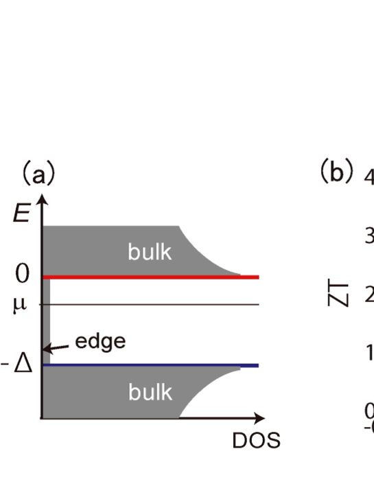
There are three carriers which contribute to : the edge electrons, bulk electrons, and phonons. We first consider an ideal situation of only edge states, while transport by the bulk electrons and phonons is neglected. The density of states is schematically described as in Fig. 1(a). We set the origin of the energy as the conduction band edge. We apply the Landauer-Büttiker formula
| (10) |
where is the channel index, is the transmission probability for the -th channel at energy , and is the Fermi distribution function [14]. In the present case, the transmission probability is equal to unity for the states with energy at , and zero otherwise, with being the size of the bulk gap. We then obtain
| (11) | |||||
| (12) |
where is the cross section of the ribbon, is an effective length of the ribbon, , and . The superscript “e” denotes the edge transport. The effective length is taken as the inelastic scattering length of the edge states . If we neglect the phonon transport, the figure of merit is
| (13) |
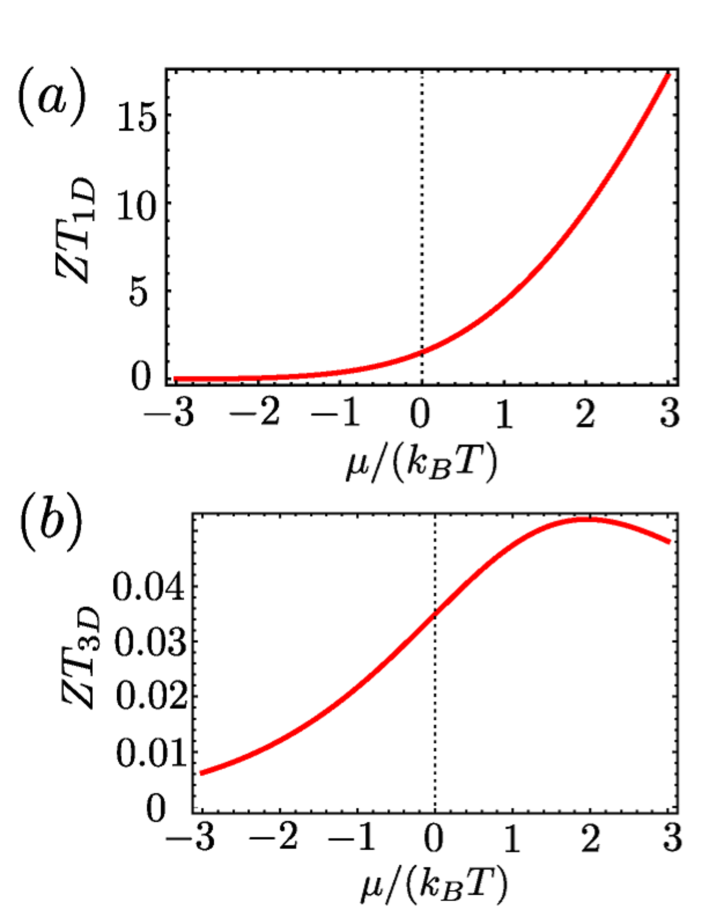
The resulting is shown in Fig. 1(b). We can see that as the chemical potential becomes larger than zero and goes into the bulk band, the increases rapidly. Compared with the ever achieved in experiments which is around , the resulting is extremely large. It is because reflects the average energy per carrier in the unit of ; if the chemical potential is in the bulk band, the edge carriers have larger energy in average, giving large .
In this regime of , the edge carriers are thermally excited holes. Therefore the carrier numbers are exponentially small, so are the transport coefficients . Hence, if we include bulk carriers or phonons, they will easily become dominant over the edge contributions, suppressing the large .
2.2 Competition between edge and bulk transport
In addition to edge transport, we consider the bulk transport. The schematic figure is shown in Fig. 2. For simplicity, we set the bulk gap to be sufficiently larger than the temperature, and the chemical potential to be near the conduction band edge. Under these assumptions the bulk valence band is neglected. We also note that we are considering very narrow ribbons, for which the transverse motion is quantized due to the confinement. For ribbons as narrow as nm wide or so, we can assume that only the first subband is involved.
Bulk transport is diffusive and calculated by the Boltzmann transport theory. For simplicity we put the lifetime to be constant.
| (14) | |||
| (15) |
where , is the number of carrier pockets, is the mobility, is the effective mass, and the superscript “b” denotes the bulk transport. The prefactors and characterize the size of the transport for the edge and the bulk, respectively, and the total transport coefficient is given by their sum:
| (16) |
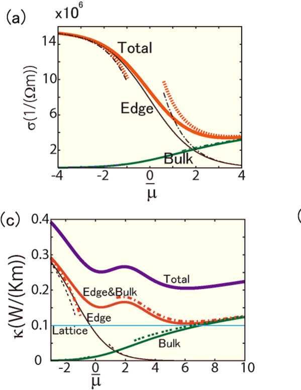
The results for the transport coefficients at K are shown in Fig. 3 (a)-(d). We took Bi2Te3 as an example [28], and adopt the parameters as , m, . The cross section of the ribbon is set to be 0.5 nm. The mobility is V-1s-1, taken from the bulk mobility at 80K [18]. For the phonon thermal conductivity we assumed Wm-1K-1 estimated from the bulk values [19, 20].
In Fig. 3, we observe interesting interplay between the edge and bulk transport. It is reasonable that in the charge conductivity (Fig. 3(a)) and the thermal conductivity (Fig. 3(c)), when the chemical potential is in the bulk gap (), the transport is dominated by edge carriers. On the other hand, when the chemical potential is in the bulk band (), the transport is dominated by bulk carriers. The behavior of the Seebeck coefficient (Fig. 3(b)) is interesting. First, the edge and bulk contributions have opposite signs. It is because the sign of the Seebeck coefficient is the same as the sign of the carriers involved. When the chemical potential is near the bulk band edge, the carriers in the bulk conduction band are electrons, whereas the carriers in the edge states are holes. Thus they have opposite contributions for the Seebeck coefficients. It is also noted that the Seebeck coefficient from the edge states is an increasing function of , while that from the bulk states is a decreasing function of . They are both asymptotically linear functions.
As a whole, the figure of merit (Fig. 3(d)) has a maximum around , the bulk band edge. We note that although the from the edge is very large when is large, it is reduced drastically by the bulk carriers and phonons. It is because in this regime of , the carrier concentration of edge states is exponentially small, and it can be easily overcome by the bulk carriers and the phonons.
We can evaluate the transport coefficients when is far from the band edge, i.e. . Here we also neglect the valence band and focus only on the conduction band and edge states, by setting . For the edge states, when (chemical potential is deep inside the bulk conduction band), the asymptotic form of is
| (17) |
and when (chemical potential is deep inside the bulk gap),
| (18) |
On the other hand, for the bulk states, when (chemical potential is deep inside the bulk conduction band), the asymptotic form of is
| (19) |
and when (chemical potential is deep inside the bulk gap),
| (20) |
From these asymptotic forms, we evaluate the asymptotics for the transport properties, shown in Fig. 3 as broken lines. In particular, the from the edge state only has the asymptotic form
| (21) | |||
| (22) |
and the from the bulk state only has the asymptotic form
| (23) | |||
| (24) |
2.3 Universal behavior described by dimensionless parameters
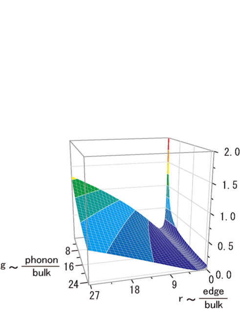
We have calculated various thermoelectric properties using specific values of parameters. There is a wide range of choices for various parameters, such as sample geometry, material choice, temperature, and so forth. It is therefore important to develop a theory which is applicable for various choices of parameters. This can be achieved by introducing dimensionless parameters and defined by
| (25) |
The parameter characterizes the ratio of edge transport to bulk transport, and characterizes the phonon transport to bulk electronic transport. The figure of merit is then expressed as a function of , and . We then maximize as a function of . In Fig. 4 we show the maximum value of for each value of and . maximum. One can see from Fig. 4 that has a minimum at . As we increase , the edge states become more and more dominant, and bulk-to-edge crossover occurs. Because the edge and bulk tend to cancel each other, this crossover is accompanied by a minimum of . In general the behavior of and as functions of the temperature is complex. Nevertheless, the inelastic scattering length is a rapidly decreasing function of , as is seen from the case of quantum Hall effect with [21], and we can estimate . Thus we conclude that by lowering temperature, edge states becomes dominant, and there occurs a bulk-to-edge crossover. The thereby has a minimum and then increases again as a function of temperature. For 10nm-wide ribbon, the crossover is expected to be around 5K-10K.
2.4 Discussion
In the above estimate, the value of is sensitive to the edge-state inelastic scattering length . If becomes longer, it is more favorable for edge-state transport since it is free from scattering up to a longer distance. It is difficult to qualitatively estimate in topological insulators because it is dominated by electron-electron scattering. We can draw analogy with quantum Hall systems, where is estimated to be 1m at 1K [21]. On the other hand, in HgTe quantum well, known as a 2D topological insulator, perfectly conducting channels for the system size 1m are observed at 1.8K, meaning that m [16]. From these data we used in our calculation.
Because is inversely proportional to the ribbon width, narrower ribbons are more favorable for edge-dominated transport, in agreement with our expectations. On the other hand, there is a minimum width for which the ribbon supports the perfectly conducting edge channels. It is determined by a penetration depth of edge states. If the ribbon width is narrower than the penetration depth of edge states, there occurs a backscattering between the edge states on the opposite sides of the ribbon, and the edge state transport is suppressed. In HgTe quantum well the penetration depth is 6nm-50nm [22, 24]. On the other hand, in some systems such as bismuth(111) 1-bilayer films, is predicted to be as short as a lattice constant [23, 24], and the ribbon can be made very narrow with keeping the perfectly conducting edge channels.
3 Thermoelectric transport by dislocations in 3D topological insulators
Compared with 2D topological insulators where the edge states are free from scattering, the surface states of 3D topological insulators undergo some scattering. In a case of Dirac cone as seen in Bi2Se3, the perfect backscattering by 180 degrees is prohibited, but other scattering processes can happen. Therefore, the surface states do not show perfect conduction.
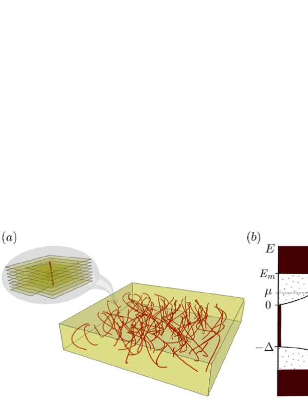
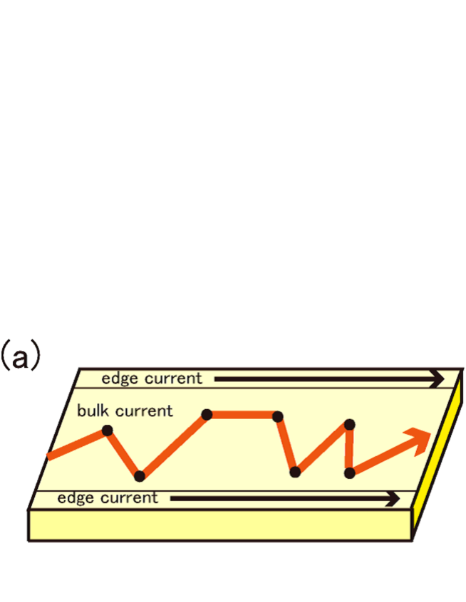
Nevertheless, it is theoretically predicted that in some of the 3D topological insulators there occurs a Kramers pair of gapless states on a lattice dislocation [8]. This state carries a pure spin current and is topologically protected. Thus these dislocations form perfectly conducting channels, as is similar to the edge states in 2D topological insulators. It is then expected that if we increase the number of dislocations, as shown in Fig. 5(a), the transport by these 1D channels becomes dominant over the bulk transport and phonon transport. Increasing the number of dislocations in the crystal is also helpful for other reasons: the mean free path of phonons is reduced by disorder, and the bulk carriers localize below the mobility edge formed at the bottom of the conduction band. Thus more dislocations enhance the 1D channel transport while at the same time suppress the bulk electron transport and phonon transport.
The framework of the calculation is similar to the 2D ribbon, and we do not provide it here. The details can be found in [10]. All the calculations are performed for room temperature, 300 K. We assume that the phonon thermal conductivity is reduced due to disorder from the bulk value of to for the average distances between dislocations nm. The gap between the valence and conduction bands is taken to be eV. We also set the mobility edge to be eV, measured from the bottom of the conduction band, see Fig. 5(b). The resulting for the 1D channel and the 3D bulk carriers are given in Fig. 6(a) and (b), respectively. As a function of the concentration of dislocations the figure of merit is calculated in Fig. 6(c). The highest value reaches when the chemical potential , which can be changed by an external gate, is near the mobility edge. Remarkably the maximum value of is over 6 at room temperature.
It is important to mention here that, if the impurities are non-magnetic, the transition to a bulk Anderson insulator should not destroy the 1D gapless states, because the time reversal invariance is not broken. Note also that by increasing the density of dislocations and/or non-magnetic impurities one can reach even greater values of . Nevertheless, these densities are less likely to be achieved and can as well result in the tunneling of electrons between the channels of neighboring dislocations. This tunneling could lead to the gap opening and localization of the protected 1D states. This is the reason for our choice of an upper limit of the dislocation density of m-2 which corresponds to an average dislocation spacing of around 3 nm.
We note that not every topological insulator has dislocations carrying 1D gapless protected modes. The condition for the 1D gapless protected modes is expressed as , where the vector (so called time-reversal-invariant momentum) is a part of the topological number for the topological insulator considered and is the Burgers vector of the dislocation [8]. Therefore, only the materials which topological numbers satisfy the above criterion can carry 1D gapless modes through the dislocations. In this sense, the dislocations in Bi2Te3 [25, 26, 27, 28] and Bi2Se3 do not carry 1D gapless modes, but the dislocations in Bi1-xSbx [29, 30] () possess 1D gapless modes.
4 Conclusion
In the present paper, we consider two types of topologically protected 1D gapless states in 2D and 3D topological insulators, as current-carrying paths for thermoelectric transport. In both cases, the 1D modes alone give large thermoelectric figure of merit , whereas the bulk states and phonons suppress the . Thus in order to have good , it is necessary to have high density of 1D modes. It is accomplished by making narrow ribbons for 2D topological insulators, and by making dislocations densely distributed in 3D topological insulators.
This work is supported partly by Grant-in-Aid for Specially Promoted Research (21000004), by Grant-in-Aid for Scientific Research iC) (22540327), by Grant-in-Aid for Global COE Program ”Nanoscience and Quantum Physics” from the Ministry of Education, Culture, Sports, Science and Technology of Japan, by NSF under Grant Nos. DMR-0547875 and 0757992, by the Research Corporation Cottrell Scholar Award, and by the Welch Foundation (A-1678).
References
References
- [1] Kane C L and Mele E J 2005 Phys. Rev. Lett. 95 226801
- [2] Kane C L and Mele E J 2005 Phys. Rev. Lett. 95 146802
- [3] Bernevig B A and Zhang S C 2006 Phys. Rev. Lett. 96 106802
- [4] Wu C J, Bernevig B A and Zhang S C 2006 Phys. Rev. Lett. 96 106401
- [5] Xu C and Moore J E 2006 Phys. Rev. B 73 045322
- [6] Fu L, Kane C L and Mele E J 2007 Phys. Rev. Lett. 98 106803
- [7] Moore E J and Balents L 2007 Phys. Rev. B 75 121306
- [8] Ran Y, Zhang Y and Vishwanath A 2009 Nature Phys. 5 298
- [9] Takahashi R and Murakami S 2010 Phys. Rev. B 81 161302(R)
- [10] Tretiakov O A, Abanov Ar, Murakami S and Sinova J 2010 Appl. Phys. Lett. 97 073108
- [11] Slack G A , in “CRC Handbook of Thermoelectrics” (Ed. D.M. Rowe) pp. 407-440, (CRC Press, Boca Raton, 1995).
- [12] Hicks L D and Dresselhaus M S 1993 Phys. Rev. B 47 12727
- [13] Mahan G D and Sofo J O 1996 Proc. Natl. Acad. Sci. U.S.A. 93 7436
- [14] Sivan U and Imry Y 1985 Phys. Rev. B 33 551
- [15] Bernevig B A, Hughes T L and Zhang S C 2006 Science 314 1757
- [16] König M, Wiedmann S, Brune C, Roth A, Buhmann H, Molenkamp L W, Qi X L and Zhang S C 2007 Science 318 766
- [17] Roth A, Brüne C, Buhmann H, Molenkamp L W, Maciejko J, Qi X -L and Zhang S -C 2009 Science 325 294
- [18] Champness C H and Kipling A L 1966 Can. J. Phys. 44 769
- [19] MacDonald D K C et al. 1959 Philos. Mag. 4 443
- [20] Zou J and Balandin A 2000 J. Appl. Phys. 89 2932
- [21] Machida T, Hirai H, Komiyama S and Shiraki Y 1996 Phys. Rev. B 54 16860
- [22] Zhou B, Lu H -Z, Chu R -L, Shen S -Q and Niu Q 2008 Phys. Rev. Lett. 101 246807
- [23] Murakami S 2006 Phys. Rev. Lett. 97 236805
- [24] Wada M, Murakami S, Freimuth F, Bihlmayer G, arXiv:1005.3912.
- [25] Hsieh D, Xia Y, Qian D, Wray L, Meier F, Dil J H, Osterwalder J, Patthey L, Fedorov A V, Lin H, Bansil A, Grauer D, Hor Y S, Cava R J and Hasan M Z 2009 Phys. Rev. Lett. 103 146401
- [26] Hsieh D, Xia Y, Qian D, Wray L, Dil J H, Meier F, Osterwalder J, Patthey L, Checkelsky L G, Ong N P, Fedorov A V, Lin H, Bansil A, Grauer D, Hor Y S, Cava R J and Hasan M Z 2009 Nature 460 1101
- [27] Zhang H J, Liu C X, Qi X L, Dai X, Fang Z and Zhang S C 2009 Nature Phys. 5 438
- [28] Chen Y L, Analytis J G, Chu J H, Liu Z K, Mo S K, Qi X L, Zhang H J, Lu D H, Dai X, Fang Z, Zhang S C, Fisher I R, Hussain Z, Shen Z X 2010 Science 325 178
- [29] Hsieh D, Qian D, Wray L, Xia Y, Hor Y S, Cava R J and Hasan M Z 2008 Nature 452 970
- [30] Nishide A, Taskin A A, Takeichi Y, Okuda T, Kakizaki A, Hirahara T, Nakatsuji K, Komori F, Ando Y and Matsuda I 2010 Phys. Rev. B 81 041309