On giant piezoresistance effects in silicon nanowires and microwires
Abstract
The giant piezoresistance (PZR) previously reported in silicon nanowires is experimentally investigated in a large number of surface depleted silicon nano- and micro-structures. The resistance is shown to vary strongly with time due to electron and hole trapping at the sample surfaces. Importantly, this time varying resistance manifests itself as an apparent giant PZR identical to that reported elsewhere. By modulating the applied stress in time, the true PZR of the structures is found to be comparable with that of bulk silicon.
pacs:
73.50.Dn, 73.50.Gr, 73.63.NmAs the most well studied and commercially important semiconductor, reports of new physical phenomena in silicon receive much attention. A recent example is giant piezoresistance (PZR) He and Yang (2006), where the change in resistance of silicon nanowires due to an applied mechanical stress was reported to be orders of magnitude larger than that of bulk silicon Smith (1954). This report is highly cited Jie et al. (2008); Neuzil et al. (2010); He et al. (2008); Barwicz et al. (2010); Reck et al. (2008); Anderås et al. (2009) in part because it may represent another example of the effect of size on the physical properties of an otherwise well characterized material Jie et al. (2008); Delmo et al. (2009); Hochbaum et al. (2008). Additionally, giant PZR is currently seen as a potential breakthrough means of detecting motion in nano-electromechanical systems He et al. (2008) where conventional detection methods lose sensitivity Mile et al. (2010); Neuzil et al. (2010); Ekinci (2005). Moreover, since mechanical stress is a key element for performance enhancement of microelectronic devices itr (2009), the physical mechanism behind giant PZR could prove to be an important ingredient in the design of future nano-scale transistors. As yet there is no consensus concerning the origins of giant PZR, although two models have some support.Cao et al. (2007); Rowe (2008) One Cao et al. (2007) is based on a surface quantization effect predicted to occur in the first few silicon monolayers, while the other Rowe (2008) is based on a stress-induced movement of the surface Fermi level in partially depleted structures resulting from a change in surface charge. The atomic length scale of the former seems to be in disaccord with the typical wire diameters reported in the literature, which are at least several tens of nanometers, whereas the characteristic length scale of the latter is the surface depletion layer width (1 nm to 10 m, depending on the doping density). It has been noted that the initially reported giant PZR occurred only in surface depleted nanowires He and Yang (2006); Rowe (2008), and subsequent claims of giant PZR involve depleted structuresNeuzil et al. (2010); Barwicz et al. (2010); Reck et al. (2008).
Here we show that in depleted structures resistance changes are dominated by electron and hole trapping at the surface. Quite unexpectedly this dielectric relaxation (which is independent of applied mechanical stress), results in apparent giant PZR signatures identical to those initially reported in silicon nanowires He and Yang (2006). The true PZR can only be measured with accuracy by modulating the mechanical stress in time as outlined below. In all cases it is comparable with that of bulk silicon Smith (1954).


A variety of unreleased and released, n-type and p-type microwires, nanowires and nanoribbons were fabricated using a top-down approach from silicon-on-insulator wafers of different device layer thicknesses () and background doping levels (see Fig. 1 and Table 1). The background doping density was chosen so that the surface depletion layer width Sze and Ng (2007) , thereby ensuring that all structures are strongly depleted. All structures were etched using deep reactive ion etching and either thermally activated phosphorous (n-type) or boron (p-type) were used as dopants for the Ohmic contacts ( cm-3). The metal contacts and tracks were composed of Ti/Au for n-type contacts and Al for p-type contacts. For released structures, the buried oxide (BOX) was removed using an HF (50 ) etch followed by supercritical CO2 drying to avoid possible wire stiction. All wires and ribbons are aligned with the crystal direction along which the mechanical stress is applied using a three-point bending method. When resistance is measured in the same direction as the applied stress, , the PZR is described by the longitudinal piezoresistive coefficient,
| (1) |
where is the change in conductance from a zero-stress value, . In the direction, Pa-1 for bulk n-type silicon and Pa-1 for bulk p-type siliconSmith (1954). On wafer, large area strain gauges were also fabricated, thereby allowing the applied stress to be monitored in-situ. The three-point bending setup, which uses a piezoelectric pusher, permits rapid and repeatable switching between zero-stress and applied stress regimes; this experimental technique is different to the usual one where applied stress is ramped or stepped monotonically with time He and Yang (2006); Neuzil et al. (2010); Barwicz et al. (2010); Choi et al. (2008). was measured by monitoring the current, , through the structures under an applied voltage, , while the silicon handle was held at a constant voltage back-gate voltage, (see Fig. 1).

The need to separate the time-varying and stress-induced resistance changes can best be illustrated with the experimental data shown in Fig. 2. At , is stepped from 0 V to 0.5 V across a 200 nm 2000 nm 30 m nanoribbon with n-type contacts, while was alternated between 0 MPa and -13.3 MPa. reduces by 27 during the initial 1000 s of measurement, and then increases for the remaining 7000 s, independent of . Using the stress modulation technique, sequential measurements of are made at zero stress (times and ) and with applied stress (times and ) (see inset). The true relative change in the conductance due to the applied stress at is found by linear interpolation to be [] which remains at a constant -0.54 (see bottom frame, Fig. 2) over time. Using Eq. 1, Pa-1, in excellent agreement with the bulk value for oriented n-type silicon Smith (1954). If the stress had been ramped linearly in time, the true PZR would have been masked by the non-stress-related drift of which is 10-100 times larger. Indeed, the implicit assumption when using a linearly-ramped stress technique is that the zero-voltage resistance remains constant for the entire measurement. As is clear from Fig. 2, this is not necessarily valid for depleted silicon structures that, as will be seen below, are sensitive to surface charging. Similar dynamic changes in the resistance of silicon nanowires have been previously reported Jie et al. (2008); Sacchetto et al. (2010); Anderås et al. (2009); Fujii et al. (1999a, b).
Figure 3a presents the results of a measurement designed to highlight how temporal changes in zero-stress resistance manifest themselves as an apparent PZR. Each solid line represents a single sweep for a particular applied stress, with swept from -1 V to 1 V in increments of 0.1 V. Two zero-stress measurements of were taken before and after the applied-stress measurement at each applied voltage, and averaged to give an accurate zero-stress reference. The applied stress was incremented between each sweep, from -13.3 MPa up to 13.3 MPa, including an applied stress of 0 MPa. The applied-stress measurements presented in this figure closely resemble published experimental data produced as evidence for giant PZR (see Fig. 2b of Ref. He and Yang, 2006), where the slope of each curve changes in step with the applied stress. However, the zero-stress reference measurements (indicated as diamonds for the first I-V sweep in Fig. 3a) indicate that the true PZR is negligible, and that the change is due solely to a non stress-related, time-dependent change in wire resistance over the duration of the measurement. Fig. 3b, which shows the apparent PZR (open triangles, calculated using the value of current at an applied stress of 0 MPa; the black line in Fig. 3a), and the true PZR (open diamonds, measured with respect to the zero-voltage reference). For clarity, the real and apparent PZRs are only depicted for an applied voltage = 0.5 V, but similar results are obtained at all voltages. The apparent PZR has an exponential dependence on like the curves obtained in Ref. He and Yang, 2006 (see Fig. 2c of that article) although other forms (including those labelled C, Z and I in Ref. 1) are observed at different moments along relaxation curves of the type shown in Fig. 2. Similarly, changes that are even larger or of opposite sign are equally possible. obtained from the apparent PZR in Fig. 3b is Pa-1 around MPa, and without use of the stress modulation technique, this value is indistinguishable from the true PZR.
By measuring the change in in response to a change in , and by assuming a linear relationship between the slope of the characteristic and the mobility, the giant PZR was attributed to a mobility variation.He and Yang (2006). This measurement is replicated using a 50 nm 50 nm 1 m p-type nanowire. The results are presented in Fig. 3c, demonstrating that the apparent mobility extracted from the slope of an measurement can also change over time independently of the applied stress. The sign and magnitude of this change is the same as the apparent stress-dependent conductance change. The true stress-dependent conductance change is consistent with bulk silicon PZR (see inset). Figure 3d shows the true values of as a function of stress obtained for four different, depleted silicon structures, together with the values expected from bulk silicon. Regardless of lateral wire size, or whether the device is released or not, the true PZR compares well with that of non-depleted, bulk silicon. Results from all measured samples can be found in Table 1.
To better understand the origin of the dynamic conductance changes, a similar approach to that used in a study of oxide traps in MOSFETs is employed, in which a measurement of the subthreshold current,
| (2) |
is made.Wang et al. (2002) Here is a constant, is the sub-threshold slope, and is the shift in the effective gate voltage due to trapped charge. at time can then be expressed as
| (3) |
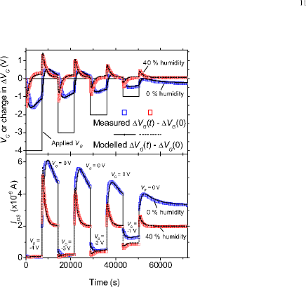
where can be measured directly from a rapid versus measurement. Measured data can then be fitted using a semi-empirical model for positive and negative charge trapping in an oxide which is based on an existing model Fischetti (2009) for positive charge trapping in SiO2 layers of metal-oxide-semiconductor (MOS) capacitors. The model assumes that the sheet density of trapped charge has a saturation value that depends linearly on the electric field across the oxide , so that where is a constant with units of cm-1V-1. approaches with a time constant , so that , where is related to the capture cross-section of the trap and the current density through the oxide Fischetti (2009); Young et al. (1979). The contribution of the trapped charge to the gate voltage is given by Fischetti (2009) , where is the oxide thickness, is the charge on an electron, and is the oxide permittivity. Figure 4 presents measured values of for a 200 nm 2000 nm 30 m n-type nanoribbon, where = 0.2 V and a series of positive and negative steps were applied to . Two sets of measurements were taken: one in a dry nitrogen atmosphere (0 relative humidity) and one in a relative humidity of . Each set of data is modelled using one type of electron (hole) trap characterised by , and (, and ). Excellent agreement is reached between the model and the measured values of over each 20-hour measurement period. The calculated current is determined by using the modelled values of in Eq. 2 and by adjusting the parameter . This closely matches the measured current as shown in the bottom frame of Fig. 4. This treatment yields several important insights into the origin of the dynamic conductance changes: i) The observed changes in current are the result of charge trapping of electrons and holes in SiO2 layers at the wires surfaces; ii) The changes in current are much more rapid at higher relative humidity, consistent with the presence of water-related charge traps Fischetti (2009); Nicollian and Brews (1982); iii) The fitted values of the constant for the hole traps (cm-1MV-1 at 0 relative humidity and cm-1MV-1 at 40 relative humidity) are almost identical to values obtained in MOS capacitor oxides Fischetti (2009); iv) Electron traps are associated with the rapid initial change in , while hole traps are associated with the slower change in the opposite direction, consistent with observations of charge trapping in MOS capacitors Young et al. (1979). This is strong evidence that the observed dynamic conductance changes are due to water-related charge traps in the oxide layer at the silicon surface. Consistent with this, the apparent giant PZR of Ref. He and Yang, 2006 was also shown to depend strongly on the characteristics of this oxide layer.
| Doping | Released? | |||||
|---|---|---|---|---|---|---|
| (nm) | (nm) | (m) | (nm) | ( /Pa) | ||
| 2000 | 2000 | 30 | 8000 | p | no | 96.6, 90, 102, 96.8, 101, 107, 87.5 |
| 2000 | 3000 | 30 | 8000 | p | no | 96.2, 102 |
| 2000 | 2000 | 30 | 8000 | p | yes | 205, 115, 125 |
| 2000 | 3000 | 30 | 8000 | p | yes | 116 |
| 100 | 50 | 1 | 800 | p | no | 58.5 |
| 75 | 50 | 1 | 800 | p | no | 74.6 |
| 50 | 50 | 1 | 800 | p | no | 76.9 |
| 200 | 2000 | 30 | 800 | n | no | -76, -77.4, -99, -48.9, -60.8, -46.3 |
| 200 | 3000 | 30 | 800 | n | no | -69.7, -50.4 |
In conclusion, charge trapping and de-trapping can mask the true PZR of depleted structures and mistakenly lead to claims of an apparent giant PZR. In more than 20 different surface depleted samples, the true PZR is found to be comparable with known values for bulk silicon (see Table 1).Beaty et al. (2002) This is in stark contrast to previous reports of giant PZR in structures of similar dimensions and doping levels. While this does not rule out giant PZR in depleted silicon structures, future claims must conclusively demonstrate that any measured resistance change be solely due to the applied stress.
References
- He and Yang (2006) R. He and P. Yang, Nature Nanotech. 1, 42 (2006).
- Smith (1954) C. Smith, Phys. Rev. 94, 42 (1954).
- Jie et al. (2008) J. Jie, W. Zhang, K. Peng, G. Yuan, C. Lee, and S. Lee, Adv. Funct. Mat. 18, 3251 (2008).
- Neuzil et al. (2010) P. Neuzil, C. Wong, and J. Reboud, Nano Lett. 10, 1248 (2010).
- He et al. (2008) R. He, X. Feng, M. Roukes, and P. Yang, Nano Lett. 8, 1756 (2008).
- Barwicz et al. (2010) T. Barwicz, L. Klein, S. Koester, and H. Hamann, Appl. Phys. Lett. 97, 023110 (2010).
- Reck et al. (2008) K. Reck, J. Richter, O. Hansen, and E. Thomsen, in IEEE 21st International Conference on Micro Electro Mechanical Systems (2008), pp. 717–720.
- Anderås et al. (2009) E. Anderås, L. Vestling, J. Olsson, and I. Katardjiev, Proc. Chem. 1, 80 (2009).
- Delmo et al. (2009) M. Delmo, S. Yamamoto, S. Kasai, T. Ono, and K. Kobayashi, Nature 457, 1112 (2009).
- Hochbaum et al. (2008) A. Hochbaum, R. Chen, R. Delgado, W. Liang, E. Garnett, M. Najarian, A. Majumdar, and P. Yang, Nature 451, 163 (2008).
- Mile et al. (2010) E. Mile, G. Jourdan, I. Bargatin, S. Labarthe, C. Marcoux, P. Andreucci, S. Hentz, C. Kharrat, E. Colinet, and L. Duraffourg, Nanotechnology 21, 165504 (2010).
- Ekinci (2005) K. Ekinci, Small 1, 786 (2005).
- itr (2009) The international technology roadmap for semiconductors (2009), URL www.itrs.net.
- Cao et al. (2007) J. Cao, X. Gong, and R. Wu, Phys. Rev. B 75, 233302 (2007).
- Rowe (2008) A. Rowe, Nature Nanotech. 3, 311 (2008).
- Sze and Ng (2007) S. Sze and K. Ng, Physics of semiconductor devices (Wiley-Blackwell, 2007).
- Choi et al. (2008) Y. Choi, T. Nishida, and S. Thompson, Appl. Phys. Lett. 92, 173507 (2008).
- Sacchetto et al. (2010) D. Sacchetto, M. Ben-Jamaa, S. Carrara, G. De Micheli, and Y. Leblebici, in Circuits and Systems (ISCAS), Proceedings of 2010 IEEE International Symposium on (IEEE, 2010), pp. 9–12.
- Fujii et al. (1999a) H. Fujii, S. Kanemaru, T. Matsukawa, and J. Itoh, Jpn. J. Appl. Phys 38, 7237 (1999a).
- Fujii et al. (1999b) H. Fujii, S. Kanemaru, T. Matsukawa, and J. Itoh, Appl. Phys. Lett. 75, 3986 (1999b).
- Wang et al. (2002) T. Wang, L. Chiang, N. Zous, T. Chang, and C. Huang, IEEE Trans. Elec. Dev. 45, 1791 (2002).
- Fischetti (2009) M. Fischetti, J. Appl. Phys. 57, 2860 (2009).
- Young et al. (1979) D. Young, E. Irene, D. DiMaria, R. De Keersmaecker, and H. Massoud, J. Appl. Phys. 50, 6366 (1979).
- Nicollian and Brews (1982) E. Nicollian and J. Brews, MOS (Metal oxide semiconductor) physics and technology (Wiley-Interscience, 1982).
- Beaty et al. (2002) R. Beaty, R. Jaeger, J. Suhling, R. Johnson, and R. Butler, IEEE Trans. Components, Hybrids, and Manufacturing Tech. 15, 904 (2002).