A Gate-Induced Switch in Zigzag Graphene Naoribbons and Charging Effects
Abstract
Using non-equilibrium Green’s function formalism, we investigate nonlinear transport and charging effects of gated graphene nanoribbons (GNRs) with even number of zigzag chains. We find a negative differential resistance (NDR) over a wide range of gate voltages with on/off ratio for narrow enough ribbons. This NDR originates from the parity selection rule and also prohibition of transport between discontinues energy bands. Since the external field is well screened close to the contacts, the NDR is robust against the electrostatic potential. However, for voltages higher than the NDR threshold, due to charge transfer through the edges of ZGNR, screening is reduced such that the external potential can penetrate inside the ribbon giving rise to smaller values of off current. Furthermore, on/off ratio of the current depends on the aspect ratio of the length/width and also edge impurity. Moreover, on/off ratio displays a power law behavior as a function of ribbon length.
pacs:
73.23.-b,73.63.-bI Introduction
Graphene is one of the intriguing new materials, which has been studied extensively since Novoselov et al.novoselov fabricated it by micromechanical cleavage in . In fact, flat structure of graphene makes its fabrication more straightforward than carbon nanotubes. Moreover, dreams of carbon nanoelectronic approach to the reality based on planar graphene structures. This structure overcomes some difficulties of nanoelectronics based on carbon nanotubes, by using lithography, one-dimensional ribbon patterns on graphene sheets experiment . For achieving realistic nanoelectronic applications based on graphene nanoribbons (GNR), width of ribbon have to be narrow enough that a transport gap is openedhan ; subtennm . Sub-10 nm GNR field-effect-transistors with smooth edges have been obtained in Ref.[subtennm, ] and demonstrated to be semiconductors with band-gap inversely proportional to the width and on/off ratio of current up to at room temperature.
The origin of transport gap which is opened in a gate voltage region of suppressed nonlinear conductance is still not well understoodMolitor ; Louie ; Castro-neto . Based on the tight-binding approach, GNRs with armchair shaped edges are either metal or semiconductorNakada ; Brey ; Louie ; Zheng . Moreover, in this approach, zigzag edge ribbons are metal regardless of their widthsOnipko . While ab initio calculationsLouie predict that regardless of the shape of the edges, GNRs are semiconductor. Two factors are responsible for transport gap: the edge disorder leading to localizationLewenkopf and the confinementNakada ; Brey ; Zheng ; Onipko . However, in nonlinear regime, transport gap is also opened by transition selection rules which originates from the reflection symmetryDuan .
Similar to carbon nanotubes, electronic transition through a ZGNRs follows from some selection rules. The rotational symmetry of the incoming electron wave function with respect to the tube axis is conserved while passing through nanotubesfarajian . Correspondingly, the transverse reflection symmetry of the incoming and outgoing wave functions results in the parity conservation in ZGNRs with even number of zigzag chainsgrosso ; beenaker ; P-Ngraphene ; duan ; kurihara ; Wakabayashi . As a consequence of the even-odd effect, a negative differential resistance (NDR) region appears in the I-V characteristic curve of P-N even ZGNR junctionsP-Ngraphene . A similar NDR behavior has been also reported in P-N nanotube junctionsfarajian . Historically, NDR was first observed in the degenerated N-P diode junctionsesaki . Nowadays, NDR has been reported in many other molecular devicesNDRgraphene ; cheraghchi .
Motivated by the work done in Ref.[subtennm, ], in this paper, we investigate nonlinear transport through gated even ZGNRs by using non-equilibrium Green’s function (NEGF) approach. The NDR region with on/off ratio of the current up to appears in the current-voltage characteristic curve. This NDR is induced by transport gaps which are opened by two selection rules governing electron transition through ZGNRs: (i) the parity conservation, and (ii) that allowed transition are between connected bandsgrosso . Based on band structure analyzing, we show that transport gap opened by the second selection rule is filled for ribbons wider than . So, sub- ribbons with long enough length provide experimental manifestation of the NDR phenomenon in I-V curve of GNRs. On the other hand, the gate voltage regulates the current flow by shifting the blocked energy regions with respect to the Fermi level. Moreover, on/off ratio of the current displays a power law behavior as a function of ribbon length as .
Our calculations show that the details of the electrostatic potential profile along the ribbon can not affect the emergence of NDR. The same conclusion has been reported by Ref.[P-Ngraphene, ], but they have not elaborated on the physical reason behind this robustness. By following the self-consistent charge and potential profiles at different voltages, we demonstrate that at low voltages, strong screening of the external potential at contacts results in a flat electrostatic potential along the ribbon. Subsequently, the e-e interaction at a mean field level, does not change the magnitude of . However, for voltages higher than the NDR threshold , the transfer of charge along the edges, leads to more reduction in which improves the switch performance.
This paper is organized as follows: although the formalism has been presented elsewherecheraghchi , to be self-contained, we briefly introduce the Hamiltonian and NEGF formalism in section II. In section III, we discuss selection rules governing even ZGNRs. The origin of NDR seen in the I-V curve is explained in section IV. We demonstrate in section V that the e-e interaction does not have a significant effect on the phenomena of NDR in the I-V curve. The last section concludes our results.
II Hamiltonian and Formalism
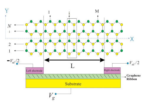
Fig.(1) shows schematic side view of graphene nanoribbon. In presence of source-drain applied potential, ribbon is divided into three regions; left, right electrodes and also central interacting region. Gate voltage is applied by means of substrate on the graphene plate. The interacting Hamiltonian governing the electron dynamics is written in tight-binding approximation. This Hamiltonian is a functional of charge density:
| (1) |
shows onsite energy of carbon atom and represents the hopping integral between nearest neighbor atoms. One orbital is considered per each site for graphene system. Without losing any generality, we set onsite energies () of all sites equal to zero. All energies are in units of . Application of a gate voltage is achieved by shifting atomic onsite energies in all three regions. The applied source-drain potential, , and the gate voltage, , preserve transverse symmetry with respect to the ribbon axis ( direction in Fig.(1)). Linear variation of the source-drain voltage along the ribbon is the solution of the Laplace equation with Dirichlete boundary condition on the contacts. is the electrostatic Green’s function and is the change in the self-consistent charge from its initial equilibrium zero-bias value. This third term is the direct Coulomb interaction created by the bias-induced charges at a mean field level which is the solution of Poisson equation. The electrostatic Green’s function for a distribution of charges between two parallel conducting planes located at which are held at zero potentialJackson , has the following form:
| (2) |
where is the Hubbard parameter whose semi-empirical value for carbonsctb is about . This parameter determines the strength of electron-electron interaction. This electrostatic Green’s function is appropriate for the kernel of Ohno-Klopmann modelok .
First of all, we must find the self-consistent charge and electrostatic potential by using NEGF formalism. The retarded and advanced Green’s function matrix subjected to the central portion of the ribbon is as the follows:
| (3) |
where . ”” is the unit matrix. are the retarded self-energies due to scattering by the left/right electrodes. These self-energies are independent of the charge density. To determine the self-energy, one needs to calculate the surface Green’s function of semi-infinite electrodes by using the Lopez-Sancho’s methodnardelli . The escaping rate of electrons to the electrodes is related to the self-energies as . Having Green’s function, one can find total charge () by separate calculations of the equilibrium and non-equilibrium charges by using the retarded and lesser Green’s functions, respectively. It is simply demonstrated that in the coherent regime, lesser Green’s function can be represented by the retarded and advanced Green’s functions which are determined in Eq.(3),
| (4) |
where shows the Fermi function of the electrodes, and show electrochemical potentials of the left and right electrodes. The initial charge is calculated by the equilibrium integration in zero bias. To obtain the charge, coupled equations of 1 and 3 are self-consistently solved by using Broyden’s methodbroyden-ohno . The transmission coefficient is defined in terms of self-consistent Green’s functions as:
| (5) |
The current passing through nanoribbon is calculated by the Landauer formula at zero temperature Liang :
| (6) |
III Band Structure and Selection Rules
To understand the transport properties of ZGNRs, one needs to study the band structure along with transmission curves. Band structure of a wide ZGNR possesses two well-separated valleys (conically-shaped dispersion curves) at and points which can be effectively described by Dirac theory. Edge states give rise to flat bands at charge neutrality point. The band structure of ZGNR is calculated in tight-binding approximation. The eigenvalues and eigenfunctions of the system are extracted by diagonalization of the following HamiltonianEzawa : ; where is the tight-binding Hamiltonian for the unit cell shown in Fig.(1). In the nearest neighbor approximation, are overlap matrices between a given cell (’0’) and its right, left neighboring cells, respectively. These matrices are dimensions where is the number of zigzag chains. The eigenvalues of this Hamiltonian, give the energy spectrum of graphene ribbon shown in Fig.(2). Here, and represent the band index and longitudinal wave vector, respectively.
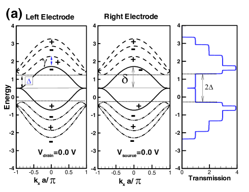
The eigenfunction can be symmetric (even parity) or asymmetric (odd parity) with respect to the mirror symmetry axis Polini . As a result of this mirror symmetry, all eigenfunctions of each band have either ’+’ or ’-’ parity, which is indicated in Fig.(2). If is even, the lowest conduction band has even parity and the highest valance band has odd parity. If the bands are labeled by the number from bottom to top as , parity of band is . In ZGNR, we consider longitudinal source-drain potentials which are invariant under mirror symmetry. Therefore, such , does not destroy the parity of the energy bands, although it changes the longitudinal momentum of electron during transport.
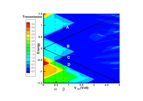
Electronic transition is controlled by two selection rules. First, the parity is conserved in tunneling of electron through even-ZGNRs. Therefore, at zero source-drain voltage, one can expect full transmission which is shown in Fig.(2.a). In this case, all bands with the same parity are energetically aligned and there is no gap in the transmission curve. In Fig.(2.a), the energy of transmission curve is shifted by the gate voltage (). Parity of each band is indicated by plus/minus signs. In the range of , there is one conducting channel which results in unit transmission coefficient. Transmission curve at could also be extracted from Fig.(4) which shows a contour plot of transmission in plane of energy and .
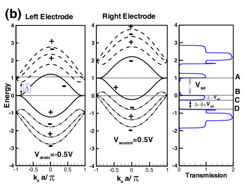
Fig.(2.b) represents band structures of electrodes which are shifted with respect to each other due to the source-drain voltage . The gap in the transmission curve of Fig.(2.b), AB region, indicates that transport between bands of opposite parity is blocked.
The second selection rule which governs electron transport through ZGNRs, is that, electron transition is allowed between connected bands. Figs.(2.a,b) show the band structure classified in three different groups; namely, central, upper and lower bands which are indicated by solid, dashed and dashed-dot-dot lines, respectively. The common feature of bands in each group is that, they are connected at the zone boundary, while distinct groups are disconnected. When one considers the electron transport, the longitudinal momentum , of electrons changes as a result of applied . The precise form of this variation in , crucially depends on profile of the superimposed longitudinal potential. These groups are disconnected from each other from the point of longitudinal momentum. Variation of momentum of electron depends on the shape of superimposed longitudinal potential. The transport properties for smoothly varying , are significantly different from profiles with sharp spatial variations. The electronic transition between an eigenstate in the right electrode and an eigenstate in the left electrode is proportional to Fourier transform of longitudinal voltage and structure factorgrosso ,
| (7) |
where structure factor of is equal to for even ZGNRs and parity of band is equal to . Parity selection rule in even ZGNRs originates from this structure factor. This parity selection rule is mesoscopic analogue of chirality factors governing transport of Dirac electrons in planar graphenekirczenow .
In our calculations, we apply a constant gate voltage to the whole system without any longitudinal variation. As a result, the gate voltage does not change momentum of electron.
However, linear variation of the applied source-drain bias (with the slope ) changes the electron momentum. So, smooth variation of the potential in longer ribbons results in a small momentum variation of electron. Consequently, transition of electron between disconnected bands is forbidden when the length of ribbon is so large that one can assume . Therefore, a smooth potential in the longitudinal direction can just scatter the electron among the class of states belonging to the same group of connected energy bands.
Now let us focus on the two transport gap regions: AB and CD in Fig.(2.b). The AB gap is a consequence of parity selection rules, while the CD gap is due to blockage of transition between disconnected groups. As can be seen in Fig.(2.b), the AB gap is proportional to the source-drain voltage, . Moreover, this gap is independent of the ribbon width. Of course, in wide ribbons, upper and lower band groups approach to the central group, especially at point , where in Fig.(2.a) tends to zero as log-normal.
When the ribbon width is increased, the separation between the upper/lower and central groups of bands, is reduced, which tends to loosen the second selection rule based on band groups; hence filling in the gaps. However when we increase the ribbon length, our classification of bands into connected groups is recovered. Therefore the AB gap is essentially governed by the aspect ratio of ZGNR.
The CD gap is equal to , where and are the energy separation of upper/lower group from the central bands at the Dirac point, and the half width of the central bands at , respectively. The dependence of on width N is: , while has a Log-Normal behavior which asymptotically approaches to the constant value of as goes up to . The conducting region BC in Fig.(2.b) can exist only, when . From the dependence of and on , the CD gap exists if is less than . Hence, NDR is estimated to be observable for ribbon width . The lowest achieved ribbon width is sub--wide ()subtennm with the length . Such long ribbons with small width provide fascinating experimental manifestation of the selection rules in transport properties.
IV Negative Differential Resistance
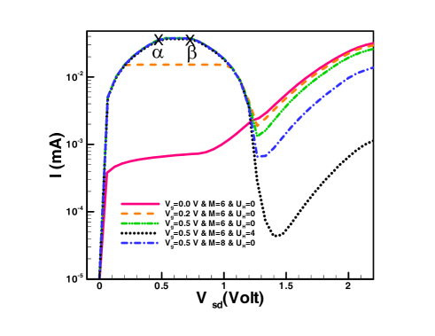
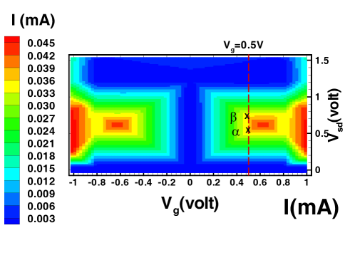
Fig.(3) shows current-voltage characteristic curve of a ZGNR with zigzag chains and unit cells in length. In the case of zero gate voltage, flow of current is blocked due to the parity selection rule, while at a given , gate bias turns the current on. After a range of in which the current remains unchanged, current begins to reduce with increasing . NDR threshold voltage decreases with gate voltage for . Dependence of NDR threshold voltage on the gate voltage can also be seen in Fig.(5). This NDR also symmetrically appears in the negative polarity of . The NDR threshold voltage and remain unchanged in the presence of the electron-electron interaction (with a given Hubbard term ). However, reduction of the current in off state, , is intensified when one takes electrostatic potential into account.
To understand the origin of NDR, it is helpful to look at the 3D contour-plot of transmission in plane of energy and which is presented in Fig.(4). Blocked energy intervals AB and CD, which are indicated in Fig.(4), correspond to those intervals shown in Fig.(2). For voltages lower than the vertical line (), transmission is a nonzero constant for the whole region of the conduction window represented in Eq.(6). As a result, current increases proportionally to . In the voltage interval , the blocked region AB, originating from the parity selection rule, contributes to the current integration window of Eq.(6). However, nonzero range of transmission remains unchanged along with resulting in the fixed current in the voltage range . So, current remains unchanged in this range. For voltages , the CD gap contributes in the current integration window, and consequently the NDR phenomenon emerges.
Regarding the importance of gate voltage in the current flow, let us investigate the effect of the gate voltage on curve by contour plotting of the current with respect to and in Fig.(4). For gate voltages , shift of transmission is not remarkable enough to contribute to conducting channels in the current integration. So, current is blocked by the parity selection rule. In the range , contribution of conducting region BC in transport is accompanied with the blockage arising from AB and CD gaps in voltages . As a consequence, current reduces after a threshold voltage. In this range, on/off ratio of the current increases and reduces with increasing the gate voltage.
As can be seen in I-V curves of Fig.(3), off current reduces for longer ribbons which enables us to achieve high performance switches by increasing aspect ratio of the ribbon length/width. The reason is connected to smooth variation of the applied potential along the ribbon such that during transport, electrons are scattered among those states which belong to continuous bands. As a consequence, blockage originating from electronic transition between disconnected bands is intensified by increasing the ribbon length. In fact, when the length of ribbon increases, transmission in the AB and CD gaps decreases exponentially.
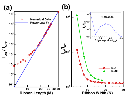
Since off current is induced by contribution of the gaps in the current integration, efficiently decreases with increasing the ribbon length (). Fig.(6.a) shows that displays a power law behavior as a function of the ribbon length for large : where . As an example, for , on/off ratio goes up to which suggests experimental fabrication of high performance switches based on the GNR nanoelectronics.
Experimentally, it was observed in Ref.[subtennm, ] that the room-temperature on/off ratio induced by the gate voltage increases exponentially as the GNR width decreases. They observed that is equal to and for and sub-, respectively. Similarly, as shown in Fig.(6.b), on/off ratio calculated for the set up considered in this paper, also decreases with the ribbon width, while reduction of on/off ratio can be compensated by considering longer ribbons. However, NDR phenomenon is disappeared for the ribbons wider than .
In ab initio calculationsLouie , by using hydrogen-termination of zigzag edges, mirror-symmetry of ZGNRs and consequently parity conservation could be retained. Correspondingly, by several repetition of the heat treatments and hydrogenation, it is also possible to create well-ordered H-terminated edges in experimentkobayashi . However, the edge states with energies about to eV have been experimentally observed kobayashi that emerge at hydrogen-terminated zigzag edges. To simulate the edge states and the effect of symmetry breaking on NDR phenomenon, it is assumed to dope one of the ZGNR edges by slight impurity. Edge impurity is considered to apply as a change in the on-site energy of the edge atoms () with respect to on-site energy of the other atoms. In case of edge disorder, plays the role of the averaged on-site energy of the edge atoms. Inset figure indicated in Fig.(6.b) shows that on/off switching reduces with the edge impurity strength, however, NDR still emerges for .
V Electrostatic potential and charging effect on NDR
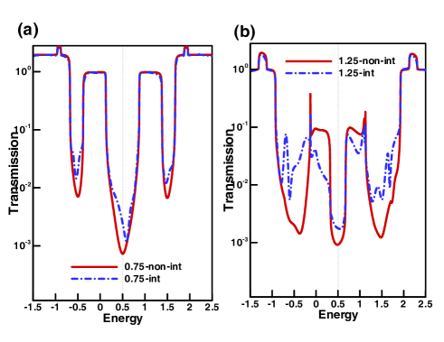
Emerging phenomenon of negative differential resistance in I-V curve is not destroyed by the e-e interaction and is independent of the details of electrostatic potential profile. However, interaction reduces off-current as shown in the I-V curves of Fig.(3). To substantiate the above claim, comparison of transmission curves in the presence and absence of the e-e interaction is useful. It is apparent from Fig.(7.a) that for voltages less than , transmission in conducting channels is robust against the e-e interaction while transmission increases in the gaps with respect to the non-interacting case. But this enhancement is slight enough which can not affect the emergence of NDR. However, for voltages , interaction lowers transmission coefficient in the conducting channels (such as BC region) in which higher subbands participate in transport. Such behavior is corroborated in Fig.(7.b) which indicates transmission at that voltage corresponding to the off-current, . Reduction in the transmission coefficient of the conducting channels results in further reduction of the off-current.
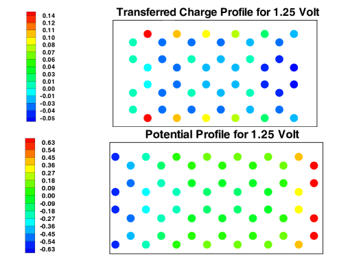
To explain the reason for such phenomenon, it is necessary to study the potential and charge profiles. Electrostatic potential averaged on each unit cell is represented in Fig.(8.a) in terms of the ribbon length. For voltages less than , potential sharply drops only at the contact regions which connects the system to electrodes. In such a case, external potential is strongly screened by redistributed electrons and, electrostatic potential of the central atoms remains close to zero. Screening is performed by discharging of electrons from the area connected to the source and their accumulation around the drain electrode. These facts are obvious from transferred charge and electrostatic potential profiles represented in Fig.9. Since determines electrostatic behavior of the potential, discharging of electrons weakens the external potential penetrated from the source electrode. Moreover, charge accumulation around the drain electrode prevents potential drop in the central part of the system. So in the case of strong screening, potential drops only at the contacts.
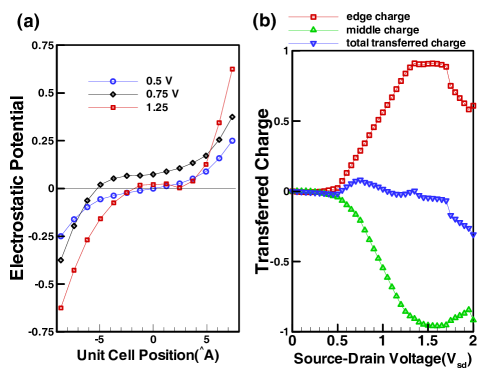
However, when the applied bias goes beyond volt, screening is being weakened and external potential can penetrate inside the central region. The reason as to why screening is weak, can be sought in charge distribution. Figure (8.b) illustrates that for voltages less than volt, in and out flow of charge are balanced with each other such that the total transferred charge remains close to zero. However, around the voltage and voltages above, the charge is mainly transferred from the edges of the ribbon, so that the source electrode does not inject further charge to middle atoms of the ribbon. As a consequence, by increasing the applied bias and so gradient of the potential along the central region, charge depletion is mainly enhanced in the middle bar area of ZGNR. On the other hand, since the only way for transporting electrons is the edge atoms, significant accumulation of charge appears along the two edge lines of ZGNR.
In summary, at voltages less than , electrostatic potential is only dropped at the contacts and therefore momentum of electrons is only varying in the area where the potential drops, while longitudinal momentum of electron remains unchanged across the central portion. In other words, potential steeply drops in the low-area district around the contacts which results in violation of the blockage rule which governs on transition between disconnected energy bands. Subsequently, transmission coefficient slightly increases in the blocked energy ranges. In other words, in this case, an increase in gradient of the potential facilitates electronic transport in the blocked energies. Note that interaction preserves transverse symmetry, so the parity selection rule still governs electronic transport. Therefore, the AB gap induced by the parity conservation still survives for voltages larger than . For voltages , electrostatic potential gradually penetrates into the whole system so that the potential of the central region is not flat. In addition, because the edge transport of electrons dominates, the transverse potential is deeper in the middle of ZGNR than its edges. Therefore, the band structure of the interacting central region differs from the band structure of electrodes. As a consequence, for voltages , transmission of conducting channels and also off current reduces.
VI Conclusion
In this paper, using non-equilibrium Green’s function approach, we investigated nonlinear transport and charging effects of graphene nanoribbons with even zigzag chains. Current flow is controlled by the gate voltage applied on the whole of sub- ribbons. In this range of widths, two selection rules govern on the electronic transition are: (i) the parity conservation, and (ii) allowed transition between connected bands. As a result, a negative differential resistance (NDR) in I-V curve is appeared in the presence of the gate voltage. Furthermore, on/off ratio of the current increases with the ribbon length as a power law behavior up to , while ribbon width and edge impurity reduce on/off ratio. Emergence of the NDR phenomenon is not sensitive to details of the electrostatic potential profile. Because of strong screening in low voltages, the major potential drop takes place at the contacts. However, in voltages larger than the NDR threshold, due to charge transfer through the ribbon edges, screening is so weak that the external potential can penetrate inside the central portion. As a consequence, off current reduces in comparison to non-interacting ribbons.
VII Acknowledges
We wish to acknowledge Prof. K. Esfarjani for collaborationcheraghchi in the development of NEGF formalism and Dr. S. A. Jafari for a critical proof-reading of the manuscript and for his useful comments and suggestions.
References
- (1) K. S. Novoselov, A. K. Geim, S. V. Morozov, D. Jiang, Y. Zhang, S. V. Dubonos, I. V. Grigorieva, and A. A. Firsov, Science 306, 666 (2004).
- (2) Z. Liu, K. Suenaga, P. J. F. Harris, and S. Iijima, Phys. Rev. Lett. 102, 015501 (2009), B. ozyilmaz, P. Jarillo-Herrero, D. Efetov, D. A. Abanin, L. S. Levitov, and P. Kim, Phys. Rev. Lett. 99, 166804 (2007).
- (3) M. Y. Han, B. ozyilmaz, Y. Zhang, and P. Kim, Phys. Rev. Lett. 98, 206805 (2007); F. Molitor, A. Jacobsen, C. Stampfer, J. G ttinger, T. Ihn, and K. Ensslin, Phys. Rev. B. 79, 075426 (2009).
- (4) X. Li, X. Wang, L. Zhang, S. Lee, H. Dai, Science, 319, 1229 (2008); X. Wang, Y. Ouyang, X. Li, H. Wang, J. Guo, H. Dai, Phys. Rev. Lett. 100, 206803 (2008).
- (5) F. Molitor, A. Jacobsen, C. Stampfer, J. G ttinger, T. Ihn, and K. Ensslin, Phys. Rev. B. 79, 075426 (2009).
- (6) Y. W. Son, M. L. Cohen, and S. G. Louie, Phys. Rev. Lett. 97, 216803 (2006).
- (7) F. Sols, F. Guinea, and A. H. Castro Neto, Phys. Rev. Lett. 99, 166803 (2007).
- (8) K. Nakada, M. Fujita, G. Dresselhaus, and M. S. Dresselhaus, Phys. Rev. B. 54, 17954 (1996).
- (9) L. Brey, H. Fertig, Phys. Rev. B. 73, 195408 (2006); Phys. Rev. B. 73, 235411 (2006).
- (10) H. Zheng, Z. F. Wang, T. Luo, Q. W. Shi, J. Chen, Phys. Rev. B. 75, 165414 (2007).
- (11) L. Malysheva and A. Onipko, Phys. Rev. Lett. 100, 186806 (2008).
- (12) E. R. Mucciolo, A. H. Castro Neto, and C. H. Lewenkopf, Phys. Rev. B. 79, 075407 (2009).
- (13) Z. Li, H. Qian, J. Wu, B-L. Gu, and W. Duan, Phys. Rev. Lett. 100, 206802 (2008).
- (14) A.A. Farajian, K. Esfarjani and Y. Kawazoe, Phys. Rev. Lett. 82, 5084 (1999).
- (15) A. Cresti, G. Grosso, G. P. Parravicini, Phys. Rev. B. 78, 115433 (2008); Phys. Rev. B. 77, 233402 (2008).
- (16) A. R. Akhmerov, J. H. Bardarson, A. Rycerz, and C. W. J. Beenakker, Phys. Rev. B. 77, 205416 (2008).
- (17) Z. Li, H. Qian, J. Wu, B. L. Gu, W. Duan, Phys. Rev. Lett. 100, 206802 (2008).
- (18) J. Nakabayashi, D. Yamamoto, and S. Kurihara, Phys. Rev. Lett. 102, 066803 (2009).
- (19) K. Wakabayashi and T. Aoki, Int. J. Mod. Phys. B. 16,4897 (2002).
- (20) Z. F. Wang, Qunxiang Li, Q. W. Shi, Xiaoping Wang, Jinlong Yang, J. G. Hou, Jie Chen, Appl. Phys. Lett. 92, 133114(2008).
- (21) L. Esaki, Phys. Rev. 109, 603 (1958)
- (22) D. Dragoman, M. Dragoman, Appl. Phys. Lett. 90, 143111 (2007).
- (23) H. Cheraghchi, K. Esfarjani, Phys. Rev. B. 78, 085123 (2008), see also its references.
- (24) S. E. Ulloa, G. Kirczenow, Phys. Rev. B. 35, 795 (1987).
- (25) J. D. Jackson, Classical Electrodynamics, 2 nd Ed , p132.
- (26) K. Esfarjani and Y. Kawazoe, J. Phys.: Cond. Matt. 1̱0, 8257 (1998).
- (27) K. Ohno, Theor. Chim. Acta 2, 219 (1964); G. Klopman, J. Am. Chem. Soc. 86, 4550 (1964).
- (28) M. B. Nardelli, Phys. Rev. B. 60, 7828 (1999).
- (29) C. G. Broyden, Math. Comput. 19, 577 (1965), also See, e.g., K. Ohno, K. Esfarjani, and Y. Kawazoe, Computational Materials Science from Ab Initio to Monte Carlo Methods (Springer, Berlin, 1999).
- (30) G. C. Liang, et al., Phys. Rev. B. 69, 115302, sec IIA (2004).
- (31) M. Ezawa, Phys. Rev. B. 73, 045432 (2006).
- (32) D. Rainis, F. Taddei, F. Dolcini, M. Polini, R. Fazio, Phys. Rev. B. 79, 115131 (2009).
- (33) Y. kobayashi, K.-I, Fukui, T. Enoki, and K. Kusakabe, Phys. Rev. B. 73, 125415 (2006); Y. Niimi, T. Matsui, H. Kambara, K. Tagami, and H. Fukuyama, Phys. Rev. B. 73, 085421 (2006).