Controlling single diamond NV color center photoluminescence spectrum with a Fabry-Perot microcavity
Abstract
We present both theoretical and experimental results on fluorescence of single defect centers in diamond nanocrystals embedded in a planar dielectric microcavity. From a theoretical point of view, we show that the overall fluorescence collection efficiency using moderate numerical aperture microscope objective can be enhanced by using a low quality factor microcavity. This could be used in particular for low temperature applications where the numerical aperture of collection microscope objectives is limited due to the experimental constraints. We experimentally investigate the control of the fluorescence spectrum of the emitted light from a single center. We show the simultaneous narrowing of the room temperature broadband emission spectrum and the increase of the fluorescence spectral density.
pacs:
78.67.Bf, 42.50.Ar, 42.55.Sa, 78.55.Hx1 Introduction
Single nitrogen-vacancy (NV) defect centers in diamond is a promising candidate for solid state quantum computing and quantum information processing (QIP) applications [1]. It has been shown that NV center can be used as a reliable source of single photons [2] for quantum key distribution (QKD) [3, 4] and single photon interferences [5]. More recently, its potentialities as a spin qubit with a very long spin coherence time [6] have been successfully demonstrated in the context of the coherent coupling of NV- electronic spin to single neighbouring nuclear spins [7, 8]. It takes advantage of both the spin coupling to optical transitions and the optical readout of the associated electron spin resonance [9]. The spin and optical properties of a single NV center were also used to probe magnetic fields at the nanoscale [10, 11].
In both QIP or QKD applications, the efficiency of the collection of the radiated photons is crucial. The rate of the qubit exchange in QKD or the efficiency of optical read-out in QIP strongly depends on the external quantum yield. To control their spontaneous emission rate or to increase their fluorescence collection, solid state individual emitters can be embedded in an optical microcavity [12, 13]. For NV center systems, different configurations of coupling with a microcavity have been investigated. Some efforts have been made in designing diamond photonic crystals microcavity [14, 15, 16]. Microcavity with a quality factors around 600 have been fabricated in a thin photonic crystals membrane [17]. Due to the difficulty to obtain monolithic microcavities from bulk or nanocrystalline diamond [18] others approaches based on hybrid structures have been used. Normal mode splitting has been observed in a system consisting of diamond nanocrystals coupled to the whispering gallery mode (WGM) of a silica microsphere [19]. The coupling of a single NV center to a high- factor WGM resonator has been observed in silica microdisk [20] or microsphere [21, 22]. By using a fiber taper, a single diamond nanocrystal has been positioned onto a silica WGM toroid which demonstrates the possibility to manipulate non-classical emitters in order to couple them with high- microresonators [23]. GaP WGM microdisk have also been used to efficiently collect at the chip scale the fluorescence of NV centers [24]. To reach very low mode volume, an optimization scheme of micropillar bragg cavity has been proposed [25]. Alternatively, hybrid structure involving photonic crystals in Silicon Nitride [26] or GaP [27] enabling coupling to NV centers have been proposed to reach high -factors. In this context the controlled coupling of a single diamond nanocrystal to a planar photonic crystal heterostructure [28] and the emission spectrum modification of a single NV center embedded in an opal photonic crystal structure made of polystyrene microsphere [29] were experimentally demonstrated. Finally one-dimensional photonic nanostructures consisting of diamond nanowires can also be used to enhance the single photon emission from NV centers [30].
In most of these previous cases, the goals were to obtain simultaneously a high-Q factors and a small mode volume in order to enhance the Purcell factor [31] and reach the regime in which the emitter spontaneous emission rate is strongly affected by its coupling to a cavity mode. This results in enhanced spectral properties of the single-photon source well adapted to GHz repetition rate QKD [32].
However, the emission rate can be not only strongly modified but also the radiation pattern of the emitter [33, 34]. The thorough investigation of the modification of the fluorescence spectrum and the radiative pattern by photonic structures is more recent, in particular for broadband emission. In that later case, the dispersion associated to its dielectric environment leads to a renormalization of the emitter spectrum, which is such that a simple planar microcavity can strongly modify the emission spectrum of an organic dye [35, 36, 37, 38] or of a colloidal CdSe/ZnS nanocrystal [39].
In this work we show that the use of a planar microcavity lead to an enhancement of the collection efficiency of the single NV center photoluminescence in practical configuration of QKD or QIP. We also demonstrate that the microcavity can be used to tune the emission spectrum. The article consists of two theoretical and experimental parts. The first part begins with the description of the planar microcavity structure. We then present the calculation method used to determine the fluorescence power collected by the microscope objective from a single NV color center located either on top of a high-reflectivity mirror or inside the microcavity. We consider both cases of the monochromatic emission (standing for cryogenic operation of the NV center emission) and the room-temperature broadband emission. In the second part, we describe the experimental setup and the observations showing the modifications of the emission associated to the coupling of a single NV color center in a nanodiamond to a single longitudinal-mode of the planar dielectric microcavity.
2 Calculation of the total fluorescence power collected from a single emitting dipole coupled to a planar Fabry-Perot microcavity
The collection of light from a single emitter embedded in a dielectric material with a high index of refraction, as NV color center in bulk diamond or semiconductor quantum dots, shares similar issues than those of semiconductor light emitting diodes (LED). They mainly come from the light trapping due to total internal reflections. A lot of theoretical and experimental studies have shown that light collection efficiency of LED can be enhanced by using a planar microcavity [40, 41]. This concept has been adapted to high index of refraction solid-state single-photon sources [13].
In the case of NV color center in diamond nanocrystals it has been pointed out that refraction is irrelevant due to the small dimensions of the nanocrystals compared to the emission wavelength and that the emitter can be assumed as a point source emitting in the surrounding dielectric medium [42]. This feature enhances the collection efficiency.
In this section we will show that the use of a resonant microcavity combined with the nanocrystal approach can also increase the collection efficiency for NV defect centers. By using a high reflectivity rear mirror the isotropic radiation is redirected in the same half space [43], while the microcavity simultaneously narrows the emission spectrum [44], both effects resulting in a larger spectral density of the collected light intensity . Finally for an appropriate choice of the emitting dipole position and orientation, one can also benefit from the local electromagnetic field enhancement [40].
2.1 Microcavity – single-emitter structure
The single-photon source described in figure 1 consists of a nanocrystal embedded in a thin polymer layer deposited on a dielectric high reflectivity (HR) Bragg mirror made of 16 periods of two materials of high and low indices of refraction [45].
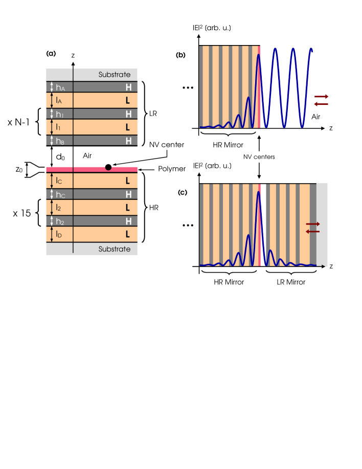
The cavity is obtained using a second low reflectivity (LR) mirror made of periods of the same materials. The resonant wavelength of the microcavity can be tuned by changing the air gap between the LR Bragg mirror and the HR mirror. The thicknesses of the different layers of the Bragg mirrors have been chosen to obtain a central wavelength around corresponding to the peak emission of the NV- center at room temperature. The structure has also been optimized to maximize the electric field amplitude in the polymer layer containing the nanocrystals. We give in figure 1 the electric field amplitude distribution for a normal incidence plane wave in the two cases we extensively study in this paper: (a) HR mirror without second mirror (b) microcavity with .
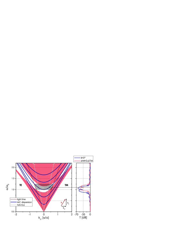
Figure 2 represents the dispersion relation of the Bragg mirrors where is the angular frequency and is the in-plane component of the wavector [46]. Due to the field penetration in the dielectric mirror the minimal interference order for the planar microcavity is given by with , and where is the floor function of [40]. With our refractive index values we obtain which is used to obtain the microcavity dispersion curves displayed in figure 2 as solid lines.
The dispersion relation is obtained noting first that . Then, if we call and the effective length and refractive index of the cavity taking into account the penetration depth in the Bragg mirrors, we obtain for a resonant mode and thus:
| (1) |
Neglecting the polymer layer effect, the two quantities and can be estimated by solving the resonance equation (for ):
| (2) |
We notice that with the microcavity design, the dispersion curve referring to is fully included in the first forbidden band of the Bragg mirror for both TE and TM polarizations and for the maximal numerical aperture considered here (i.e. N.A.=1, corresponding to the light line) and thus also for the value N.A.=0.6 used in the experiments. This feature is important for room temperature experiments since in this case the fluorescence spectrum of NV centers is broad (full width at half maximum FWHM) and therefore requires a broadband operation range. We also show the transmission spectrum obtained using the standard transfer matrix method [46] for a microcavity with both for the normal incidence, and for TM polarization cases. Note that due to the unbalanced mirror reflectivity, the resonant transmission is weak even though we assumed lossless materials.
This simple linear analysis [13] allows two properties of the microcavity to be revealed: i) for the numerical aperture N.A.=0.6 used in our experiment it is possible to efficiently collect light coupled to the resonant mode of the cavity, ii) in the case of a broadband emission, the blue-shift of the cavity resonance explains the spectrum asymmetry experimentally observed (see Section 3).
2.2 Calculation method of the total collected power radiated by a single NV color center inside the microcavity
It is well established since the early studies of NV- color center [47], that it has two orthogonal incoherent electric dipole transitions oriented in the plane perpendicular to the [111] crystallographic direction (along the N-V axis), as exemplified in the context of recent studies on polarization selective excitation of this color center [48, 49].
In the following we will model the NV- center by two identical orthogonal dipoles . The dipoles are assumed to be located in O. orientation is defined by two angles and relative to the Bragg mirror plane , such as in the sample plane coordinate system as represented in figure 3. Thus the second dipole can be written: with and . The most favorable configuration to efficiently collect the photoluminescence of the NV- color center corresponds to whereas the worst configuration is obtained for . In the experiment we selected the brightest emitters, which are the one having the strongest in-sample plane dipole components. Therefore, in the following we restrict our calculation of the collected power to this configuration . To calculate the power radiated by the two dipoles in the upper half space (), we used the transfer-matrix method of reference [50].
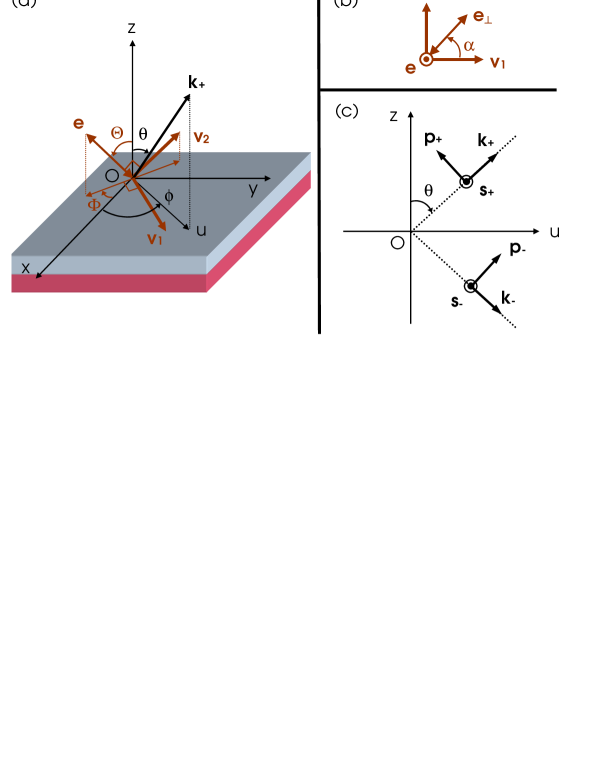
For a given direction of radiation characterized by the wavevector , with coordinate , the wave can be either TE-polarized along or TM-polarized along . is the unit vector orthogonal to the incidence plane , whereas is calculated by:
| (3) |
The wavevector of the field related to propagating in the opposite direction is noted . We also have and the same relation as Eq. (3) holds for . According to the method given in reference [50] and using the dipole description of references [34] and [51] the source terms for the two propagation directions are:
| (4) |
We have the same relations for . Using these expressions for the optical sources it is possible to calculate the spectral density of the radiated power per solid angle for a given by summing the power emitted by the two incoherent dipoles [50]. Following the method described in reference [37], the full radiated power collected by the air microscope objective of numerical aperture N.A.= in a spectral window of full width is then evaluated by :
| (5) |
where is the free space emission normalized spectrum function which will be assumed for simplicity to have a Gaussian profile centered at with a full width at half maximum .
2.3 Calculation of
Our aim is to show that the light extraction from a single emitter can be increased using a low finesse microcavity in practical cases. Consequently we will take as the reference the case of dipoles located on a single mirror. The advantage of this last configuration with respect to free space is twofold: the mirror redirects the fluorescence in the same half space and if the dipoles are located in a field antinode, their emission rate is increased [40, 43]. In the following we consider two cases: 1) the monochromatic emission of NV- at its zero-phonon line (ZPL) wavelength nm, which corresponds to cryogenic operation, 2) the broadband emission case, associated to room-temperature photoluminescence.
2.3.1 Monochromatic case
First we focus on the low temperature configuration. In this particular case, the fluorescence spectrum of the emitter is assumed to be quasi-monochromatic and the ZPL has a bandwidth around nm [52, 53]. For simplicity and because our cavity has been optimized for a resonant wavelength , we have used for the calculation as the emission wavelength instead of .
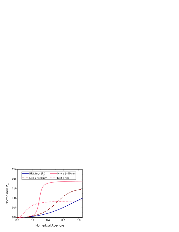
In order to collect the light across the fused silica substrate of the LR mirror in the case of the microcavity configuration, we use a long working distance objective with a numerical aperture N.A.=0.6. The reference configuration consists of a HR mirror and a microscope objective with N.A.=0.85. We used this low value of N.A. because it is suited to cryogenic setup [52]. The simulation results are shown in figure 4. In the case of low finesse cavity () and a detuning nm, we observe an increase of about in the collection efficiency with respect to the reference case. This can be increased by using a better finesse () cavity (). Note that in this case, the cavity must be slightly positively detuned () to obtain the maximal collection increase of about . This positive detuning allows the spectral overlap between the emission spectrum and the microcavity dispersion to be optimized as illustrated by the hatched area in figure 2. For we do not observe any increase in the extracted fluorescence for the maximal numerical aperture.
2.3.2 Broadband emission
At room temperature, the coupling between the radiative transitions of the NV- color center and the diamond matrix phonon broadens the emission spectrum yielding a FWHM linewidth of about nm due to the phonon replica.
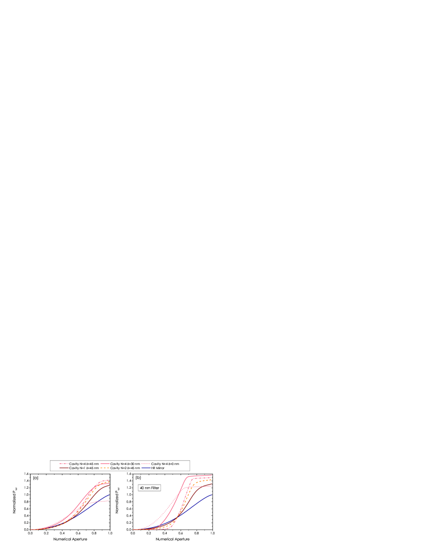
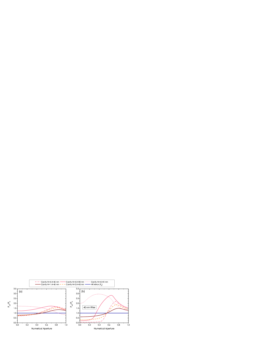
Figure 5.(a) gives the calculation of the full radiated power with no additional filter whereas figure 5.(b) represents the same calculations with a band-pass filter whose resonant wavelength is chosen in order to increase the overall radiated power for the maximal numerical aperture. This filter could be useful for example in open space QKD applications where it will reject a large amount of background light [4]. As it was the case for monochromatic emission the enhancement is better for and for a positive detuning. The maximal enhancement is weaker than in the previous configuration since in room temperature experiments it is possible to use larger numerical aperture collection objectives with N.A. close to unity. Note that the collection efficiency enhancement is improved by the band-pass filter as shown in figure 5.(b). This effect comes from the increase of the coherence length due to the coupling of emitted light to the microcavity mode, similarly to what has already been observed in microcavity LED [54]. We can underline furthermore this phenomenon by calculating the enhancement ratio where is the radiated power by the HR mirror at the same N.A. than the one used to calculate . The corresponding results are shown in figure 6.(a) for the full spectrum and (b) for the filtered spectrum. We note that the maximal collection efficiency is reached for N.A.. For N.A.=0.6 and detuning the maximal enhancement is increased by 1.7 for the full bandwidth detection [figure 6.(a)] and by 2.75 for the filtered detection [figure 6.(b)].
At low N.A. and filtered detection, the collected power is reduced in the microcavity case () with respect to the mirror case for detuning larger than . This situation is reversed if one uses smaller detuning values as can be seen for and in figure 6.b). Indeed for low numerical apertures a large positive detuning has a detrimental role since the cavity resonance would be obtained for too large angles of incidence, out of the collection aperture.
Finally we have also calculated that for N.A. and the configuration / the total collected power in the case of the filtered detection is larger than the full bandwidth detection one with only the HR mirror.
Note that the evolution of vs N.A. obtained for the optimal NV color center dipoles orientation holds for all possible orientations. For broadband emission, in the worst configuration , and in the case of a numerical aperture , the same calculation methods yields a total collected power equal to 53% of the one of the best configurationin the case of the HR Bragg mirror. Similar results are obtained in the case of a microcavity, for which the total collected power in the worst dipole orientation case corresponds to 50% of total power in the optimal case.
As a conclusion the simulation shows that the collection of photoluminescence from a single NV- color center can be increased by its coupling to one low order mode of a planar microcavity. Even in the case of broadband emission the use of a moderate finesse () can enhance the collection efficiency. In addition such coupling also lead to a narrowing of the emitted spectrum and thus to an increase in the coherence length of the emitted light.
3 Experimental measurement of the spectral properties of the NV color-center coupled to a single mode of the planar microcavity
3.1 Experimental setup
The single emitter studied in this work is a NV- color center in type 1b (natural specified content in nitrogen ppm) diamond nanocrystals (Micron+ MDA 0-0.1 from De Beers/Element6) with a size smaller than 100 nm, obtain by a high-pressure and high temperature synthesis. In order to increase the natural content of NV center in the nanodiamonds, the particle were irradiated by a high-energy electron beam to generate vacancies and then annealed during 2 hours at under vacuum. Then, they were cleaned by oxydative chemicals and dispersed in a propanol solution containing a polymer at low concentration (polyvinylpyrrolidone, w/w). The mean hydrodynamical size of the nanodiamond in the colloidal suspension is 90 nm as measured by dynamic light scattering. The nanodiamond–polymer solution is finally spincoated onto the HR dielectric mirror forming a thick polymer layer with a surface concentration of about one nanocrystal per . The microcavity is obtained by placing a LR mirror ( reflectivity, RLR 90 ) in front of the HR mirror (reflectivity RHR 99.99 ) at a distance that can be adjusted using micrometric screws and piezoelectric actuators. From an experimental of view, the actual values of layer thicknesses for the HR mirror are: and .
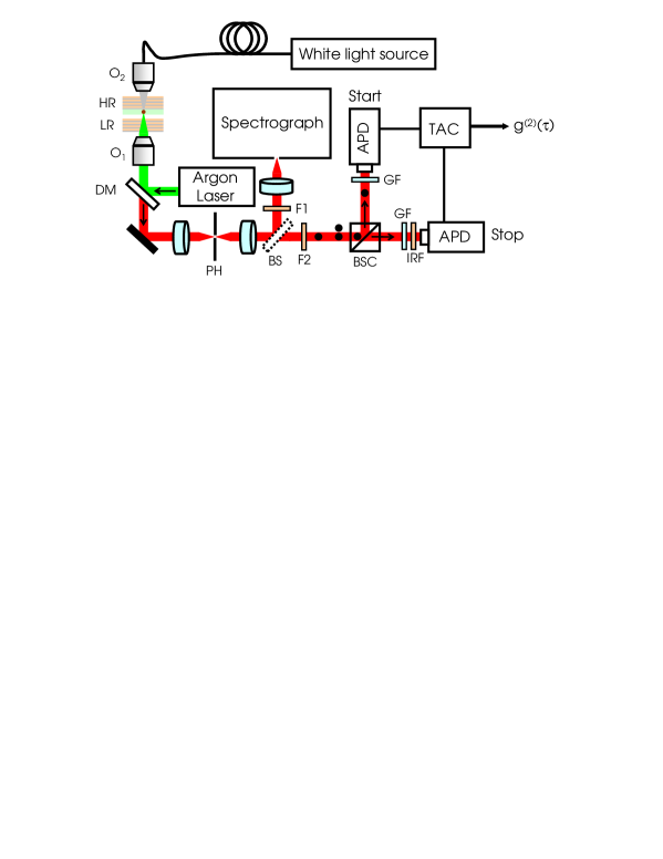
Figure 7 is a schematic of the confocal optical scanning microscope [56] used to study the fluorescence of a single NV center in a dielectric microcavity. The light at wavelength from a cw argon-ion laser is focused on the nanodiamond-polymer layer through the LR mirror, with a long working distance microscope objective O1 having a N.A.=0.6. The objective is corrected for the fused silica substrate of the LR mirror. Nevertheless, its optical characteristics can be switched, which allows it to be used without the additional LR mirror. The LR mirror has a reflectivity less than in the range allowing for efficient excitation at the laser wavelength. The sample is raster scanned with a piezoelectric stage. The fluorescence from NV centers is collected through the same objective O1, the detection volume being defined by a confocal pinhole. The collected light passes through a dichroic mirror and long-pass filters are used to remove any residual excitation light. The fluorescence light intensity is equally divided into a first beam for spectral analysis by an imaging spectrograph (composed of a grating and a cooled CCD array for spectrum record) and a second beam for measuring the photon statistics using the standard Hanbury-Brown and Twiss (HBT) coincidence setup. The latter measurement allows us to identify the emission of a single color center yielding a perfect photon antibunching. The white light source and the microscope objective O2 are used to measure the microcavity transmission spectrum. Note that in our experimental configuration we obtain a transmission spectrum averaged over the numerical aperture of and over the two polarizations TE and TM as detailed in A.
3.2 Narrowing of the spectrum of a single NV- color center coupled to one microcavity mode
To identify well isolated fluorescent emitters, we first raster scan the sample. For each fluorescent spot, the uniqueness of the emitter is then checked by the observation of antibunching in the photon statistics of the fluorescent light. Since after the emission of a first photon, it takes a finite time for a single emitter to be excited again and then it spontaneously emits a second photon, the antibunching effect appears as a dip around zero delay in the normalized intensity time autocorrelation function:
| (6) |
The HBT detection setup allows one to record the histogram of time delays between two consecutively detected photons on each APD. Considering our detection efficiency of a few percentages, this histogram is a very good approximation of the intensity autocorrelation function .
Figure 8 shows different emission spectra measured for the same single NV center while changing the cavity length. The first spectrum at the bottom is obtained for a closed cavity (i.e., HR and LR mirror into optical contact). In this configuration there is no resonant mode in the Bragg mirror stop-band and the fluorescence of the center is inhibited.
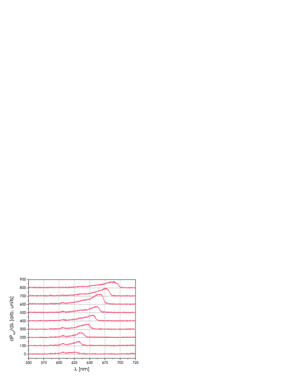
By opening the cavity we increase the resonant wavelength corresponding to and we obtain a resonant mode whose wavelength is located inside the emission spectrum of the NV- center. We observe that the emitted fluorescence intensity is maximal with a noticeable shrinking of the spectrum, when the resonant wavelength is slightly detuned from the free space NV- center emission maximum (see third curve starting from top of figure 8).
Figure 9.(a) shows the detailed analysis of one of the optimal configurations. The experimental transmission has been measured and this optimal case corresponds to the situation where the cavity resonant wavelength is almost tuned at the emission maximum. Here, the optimal detuning is almost zero since the experimental value of N.A. is only 0.6. Figure 9.(b) displays the cavity emission spectrum and the HR mirror emission spectrum (used as reference) recorded in the same experimental conditions. In particular the saturation of the single NV center has been reached for the two configurations. Finally figures 9.(c) and 9.(d) are time intensity second order correlation functions associated to the emission of single NV center, for the mirror and cavity configurations respectively. The vanishing dip at zero delay in the function insures that we address single color center in both cases.
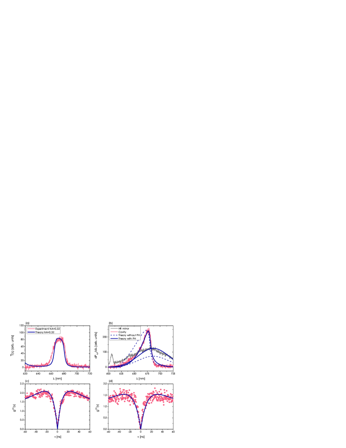
The fit of the transmission spectrum of the cavity as been obtained only adjusting the value of the air gap thickness (here and thus ) governing mainly the resonant wavelength value. As mentioned in A, we consider that the numerical aperture value is limited by the illumination objective (N.A.=0.32). The spectral width of the calculated linear transmission spectrum is in good agreement with the experimental results. For the comparison between the experimental and theoretical fluorescence spectra, we had to take into account the characteristics of our confocal microscope. Indeed, it is not possible to reproduce the width and the amplitude of the experimental spectra only using the expression of the overall radiated power derived from equation (5). This is illustrated by the dash theoretical curves of figure 9.(b). We have normalized the theoretical calculations using the maximum of the microcavity spectrum. In this case the theoretical HR mirror emission spectrum, normalized in the same way, does not fit the experimental data. The confocal aperture spatial filtering must be taken into account to obtain a good agreement between the theory and the experimental results [59]. The model used to simulate the propagation across the microscope is described in B. After fixing the value of obtained from the transmission spectrum fit, the defocusing (see B) is the only adjustable experimental parameter. Note that we have already mentioned that we have experimentally selected the brightest emitters whose the two orthogonal dipoles are parallel to the mirror plane. Consequently we assume in the following calculations that and as it was the case in the theoretical part. The diameter of the confocal aperture is well adapted for the case of an emitter deposited on the HR mirror. In this case, the pinhole does not truncate the electric field distribution and we obtain an almost perfect collection efficiency for . Calculations show that for an emitter inside the cavity, the pinhole diameter is not perfectly adapted. The collection efficiency is thus reduced with respect to the case of the HR mirror. This detrimental effect could be reduced by using a larger confocal aperture. The effect of the LR mirror on the imaging properties of the system is taken into account by using a negative defocusing [60]. The theoretical calculations given in figure 9.(b) have been carried out using a defocusing almost corresponding to the optimal value for the overall signal collection. In this case, we obtain a very good agreement simultaneously for the shape of the spectrum and for the relative amplitude between the reference (HR mirror) and the microcavity.
We show that the spectrum of a single NV center can be tailored using a planar microcavity in a similar way than for single molecules [38]. From a qualitative point of view, the fluorescence spectrum is asymmetric and shows profile steepening from its red side which is in good agreement with other experimental observations in microcavity LEDs [61]. We also show a good agreement between the experimental results and the theoretical calculations taking into account the optical and geometrical properties of our experimental setup.
We then compared the performances of the sole HR mirror single-photon source, to the one with the emitter inside the microcavity.
-
Configuration Excitation laser Total photon Counting rate spectral power counting rate density around HR mirror 11.5 mW 140 kcounts/s 0.5 counts/s/nm Microcavity 10.2 mW 63 kcounts/s 1.0 counts/s/nm
Table 1 reports the total counting rates (sum of both APDs), and the counting rate spectral density for the two configurations at similar input excitation laser power. We measured 140 kcounts/s for the HR mirror configuration and 63 kcounts/s in the case of the microcavity. We thus observe a reduction of between the HR mirror and the cavity case. The theory gives only a reduction of due to the pinhole effect. The difference might come from the filtering of the parasitic light (e.g. Raman scaterring) in the case of the cavity. Note that we would have obtained an augmentation of without taking into account the pinhole filtering. We however observed an interesting modification of the fluorescence in the cavity configuration: due to the narrowing of the emitted spectrum from nm to nm, the counting rate spectral density is twice larger in the microcavity case, which proves that the emission modes of the nanocrystal are to some extent coupled to some microcavity modes for which the fluorescence rate is enhanced.
4 Conclusion
We have shown theoretically using a simple dipole model embedded in a multilayer system that the fluorescence collection of a single NV diamond color center can be enhanced by a factor of two when it is placed into a moderate finesse () microcavity with respect to its emission when it is located onto a single HR mirror. The calculations have been done in practical configurations of either Quantum Key Distribution corresponding to a room temperature operation and thus broadband emission of the NV center, or of Quantum Information Processing associated to cryogenic temperatures and monochromatic emission at the zero-phonon line wavelength. We also performed room temperature experiments using NV color center in diamond nanocrystals and studied the effect of a planar microcavity on the detected fluorescence light from a single NV center. We have shown that the fluorescence spectrum can be narrowed using such a planar microcavity and that the counting rate spectral density can be increased compared to the use of a single HR mirror. Such simultaneous spectrum narrowing and fluorescence spectral density enhancement brought by the microcavity represent a significant increase in the performances of the diamond NV color center based single-photon source in the prospects of open-air QKD applications.
Appendix A Linear transmission calculation in the case of a focused illumination
We give here the expression of the averaged transmission spectrum of the microcavity used to reproduce the experimental results. We used the standard linear transmission calculated for a plane wave propagating in the direction with a polarization using the transfer matrix method [46] to evaluate the quantity:
| (7) |
We assume that the beam limitation only comes from the numerical aperture of the microscope objective used to illuminate the microcavity with the white light as shown in figure 7 and thus .
Appendix B Theoretical description of the propagation in the imaging system
In this section we give the method used to take into account the effect of the confocal aperture (diameter ) and the defocusing on the collection efficiency. The defocusing is taken into account by adding a perturbation to a reference wave surface propagating in our stigmatic optical system as represented in figure 10 [62, 63]. We consider here three wave surfaces: i) which is the object focal sphere of radius ii) a plane wave surface located in the intermediary space between the microscope objective (focal ) and its tube lens of focal and iii) the image focal sphere of radius .
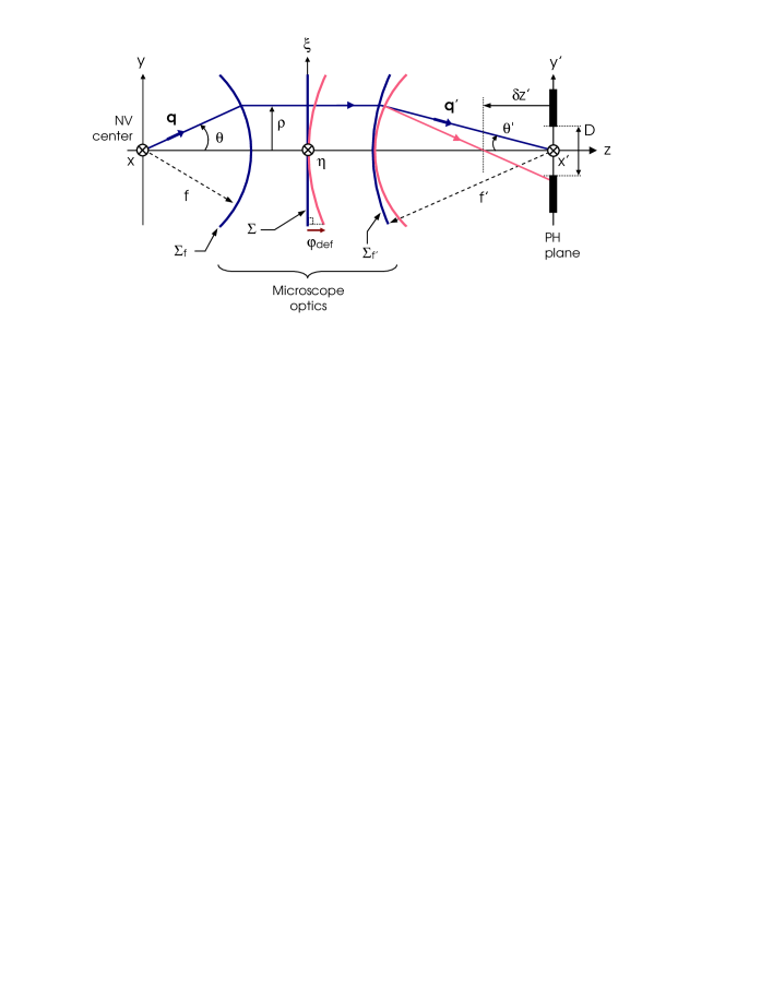
We assume a perfect imaging system and these three surface waves are stigmatic. First we calculate the field (where we note ) in the direction on the reference sphere using equations (4). Then we obtain the electric field on the plane wave surface [64]:
| (8) |
where and are the coordinates of the intersection between the emerging ray and . For a given direction characterized by and the unitary vector , we can write the emerging field on the surface :
| (9) |
The additional phase term accounts for the image space defocusing :
| (10) |
For a given object aperture angle , the corresponding image angle is calculated using: where [64]. The defocusing value in the image space is connected to the defocusing in the object space using the sine and Herschel conditions noting that where is the magnification of the objective . In the image space, the numerical aperture is weak and the paraxial approximation can be used. In particular, the electric field in the focal plane can be calculated using a Fourier Transform (FT):
| (11) |
References
References
- [1] Ladd T D, Jelezko F, Laflamme R, Nakamura Y, Monroe C and O’Brien J L 2010 Quantum computers Nature 464 45–53
- [2] Kurtsiefer C, Mayer S, Zarda P and Weinfurter H 2000 Stable solid-state source of single photons Phys. Rev. Lett.85 290–293
- [3] Beveratos A, Brouri R, Gacoin T, Villing A, Poizat J-P and Grangier P 2002 Single photon quantum cryptography Phys. Rev. Lett.89 187901
- [4] Alléaume R, Treussart F, Messin G, Dumeige Y, Roch J-F, Beveratos A, Brouri-Tualle R, Poizat J-P and Grangier P 2004 Experimental open-air quantum key distribution with a single-photon source New J. Phys.6 92
- [5] Jacques V, Wu E, Grosshans F, Treussart F, Grangier P, Aspect A and Roch J-F 2007 Experimental realization of wheeler’s delayed-choice gedanken experiment Science 315 966–968
- [6] Kennedy T A, Colton J S, Butler J E, Linares R C and Doering P J 2003 Long coherence times at 300 K for nitrogen-vacancy center spins in diamond grown by chemical vapor deposition Appl. Phys. Lett. 83 4190–4192
- [7] Jelezko F, Gaebel G, Popa I, Domhan M, Gruber A and Wrachtrup J 2004 Observation of coherent oscillation of a single nuclear spin and realization of a two-qubit conditional quantum gate Phys. Rev. Lett.93 130501
- [8] Childress L, Gurudev Dutt M V, Taylor J M, Zibrov A S, Jelezko F, Wrachtrup J, Hemmer P R and Lukin M D 2006 Coherent dynamics of coupled electron and nuclear spin qubits in diamond Science 314 281–285
- [9] Jelezko F, Gaebel T, Popa I, Gruber A and Wrachtrup J 2004 Observation of coherent oscillations in a single electron spin Phys. Rev. Lett.92 076401
- [10] Balasubramanian G, Chan I Y, Kolesov R, l-Hmoud M, Tisler J, Shin C, Kim C, Wojcik A, Hemmer P R, Krueger A, Hanke T, Leitenstorfer A, Bratschitsch R, Jelezko F and Wrachtrup J 2008 Nanoscale imaging magnetometry with diamond spins under ambient conditions Nature 455 648–652
- [11] Maze J R, Stanwix P L, Hodges J S, Hong S, Taylor J M, Cappellaro P, Jiang L, Gurudev Dutt M V, Togan E, Yacoby A, Zibrov A S, Walsworth R L and Lukin M D 2008 Nanoscale magnetic sensing with an individual electronic spin in diamond Nature 455 644–647
- [12] Moreau E, Robert I, Gérard J-M, Abram I, Manin L and Thierry-Mieg V 2001 Single-mode solid-state single photon source based on isolated quantum dots in pillar microcavities Appl. Phys. Lett. 79 2865–2867
- [13] Barnes W L, Björk G, Gérard J-M, Jonsson P, Wasey J A E, Worthing P T and Zwiller V 2002 Solid-state single photon sources: light collection strategies Eur. Phys. J. D 18 197–210
- [14] Tomljenovic-Hanic S, Steel M J, de Sterke C M and Salzman J 2006 Diamond based photonic crystal microcavities Opt. Express 14 3556–3562
- [15] Kreuzer C, Riedrich-Möller J, Neu E and Becher C 2008 Design of photonic crystal microcavities in diamond films Opt. Express 16 1632–1644
- [16] Tomljenovic-Hanic S, Greentree A D, de Sterke C M and Prawer S 2009 Flexible design of ultrahigh-Q microcavities in diamond-based photonic crystal slabs Opt. Express 17 6465–6475
- [17] Wang C F, Hanson R, Awschalom D D, Hu E L, Feygelson T, Yang J and Butler J E 2007 Fabrication and characterization of two-dimensional photonic crystal microcavities in nanocrystalline diamond Appl. Phys. Lett. 91 201112
- [18] Wang C F, Choi Y-S, Lee J C, Hu E L, Yang J and Butler J E 2007 Observation of whispering gallery modes in nanocrystalline diamond microdisks Appl. Phys. Lett. 90 081110
- [19] Park Y-S, Cook A K and Wang H 2006 Cavity QED with diamond nanocrystals and Silica microspheres Nano Lett. 6 2075–2079
- [20] Fu K-M, Santori C, Spillane S M, Fattal D, Xu Q, Fiorentino M, Beausoleil R G, Barclay P E and Painter O 2008 Coupling single NV centers in diamond to optical microcavities Conference on Lasers and Electro-Optics/Quantum Electronics and Laser Science Conference and Photonic Applications Systems Technologies, OSA Technical Digest paper JMB3.
- [21] Schietinger S, Schröder T and Benson O 2009 One-by-one coupling of single defect centers in nanodiamonds to high-Q modes of an optical microresonator Nano Lett. 8 3911–3915
- [22] Schietinger S and Benson O 2009 Coupling single NV-centres to high-Q whispering gallery modes of a preselected frequency-matched microresonator J. Phys. B: At. Mol. Opt. Phys.42 114001
- [23] Gregor M, Henze R, Schröder T and Benson O 2009 On-demand positioning of a preselected quantum emitter on a fiber-coupled toroidal microresonator Appl. Phys. Lett. 95 153110
- [24] Barclay P E, Fu K-M, Santori C and Beausoleil R G 2009 Chip-based microcavities coupled to nitrogen-vacancy centers in single crystal diamond Appl. Phys. Lett. 95 191115
- [25] Zhang Y and Lončar M 2009 Submicrometer diameter micropillar cavities with high quality factor and ultrasmall mode volume Opt. Lett. 34 902–904
- [26] McCutcheon M W and Lončar M 2008 Design of a silicon nitride photonic crystal nanocavity with a Quality factor of one million for coupling to a diamond nanocrystal Opt. Express 16 19136–19145
- [27] Barclay P E, Fu K M, Santori C and Beausoleil R G 2009 Hybrid photonic crystal cavity and waveguide for coupling to diamond NV-centers Opt. Express 17 9588–9601
- [28] Barth M, Nüsse N, Löchel B and Benson O 2009 Controlled coupling of a single-diamond nanocrystal to a photonic crystal cavity Opt. Lett. 34 1108–1110
- [29] Stewart L A, Zhai Y, Dawes J M, Steel M J, Rabeau J R and Withford M J 2009 Single photon emission from diamond nanocrystals in an opal photonic crystal Opt. Express 17 18044–18053
- [30] Babinec T M, Hausmann B J M, Khan M, Zhang Y, Maze J R, Hemmer P R and Lončar M 2010 A diamond nanowire single-photon source Nat. Nanotechnol. 5 195–199
- [31] Purcell E M 1946 Spontaneous emission probabilities at radio frequencies Phys. Rev.69 681
- [32] Su C-H, Greentree A D and Hollenberg L C L 2008 Towards a picosecond transform-limited nitrogen-vacancy based single photon source Opt. Express 16 6240–6250
- [33] Drexhage K H 1970 Influence of a dielectric interface on fluorescence decay time J. Lumin. 1-2 693-701 (1970)
- [34] Lukosz W 1979 Light emission by magnetic and electric dipoles close to a plane dielectric interface. III. Radiation patterns of dipoles with arbitrary orientation J. Opt. Soc. Am.69 1495–1503
- [35] Enderlein J 2002 Spectral properties of a fluorescing molecule within a spherical metallic nanocavity Phys. Chem. Chem. Phys. 4 2780–2786
- [36] Steiner M, Schleifenbaum F, Stupperich C, Failla A V, Hartschuh A and Meixner A J 2005 Microcavity-controlled single-molecule fluorescence ChemPhysChem 6 2190–2196
- [37] Steiner M , Failla A V, Hartschuh A, Schleifenbaum F, Stupperich C and Meixner A J 2008 Controlling molecular broadband-emission by optical confinement New J. Phys.10 123017
- [38] Chizhik A, Schleifenbaum F, Gutbrod R, Chizhik A, Khoptyar D, Meixner A J and Enderlein J 2009 Tuning the fluorescence emission spectra of a single molecule with a variable optical subwavelength metal microcavity Phys. Rev. Lett.103 073002
- [39] Qualtieri A, Morello G, Spinicelli P, Todaro M T, Stomeo T, Martiradonna L, De Giorgi M, Quélin X, Buil S, Bramati A, Hermier J-P, Cingolani R and De Vittorio M 2009 Nonclassical emission from single colloidal nanocrystals in a microcavity: a route towards room temperature single photon sources New J. Phys.11 033025
- [40] Benisty H, De Neve H and Weisbuch C 1998 Impact of planar microcavity effects on light extraction – Part I: basic concepts and analytical trends J. Quantum Electron. 34 1612–1631
- [41] Benisty H, De Neve H and Weisbuch C 1998 Impact of planar microcavity effects on light extraction – Part II: selected exact simulations and role of photon recycling J. Quantum Electron. 34 1631–1643
- [42] Beveratos A, Brouri R, Gacoin T, Poizat J-P and Grangier P 2001 Nonclassical radiation from diamond nanocrystals Phys. Rev. A 64 061802
- [43] Begon C, Rigneault H, Jonsson P and Rarity J G 2000 Spontaneous emission control with planar dielectric structures: an asset for ultrasensitive fluorescence analysis Single Mol. 1 207–214
- [44] Rigneault H and Monneret S 1996 Modal analysis of spontaneous emission in a planar microcavity Phys. Rev. A 54 2356–2358
- [45] Beveratos A, Kühn S, Brouri R, Gacoin T, Poizat J-P and Grangier P 2002 Room temperature stable single-photon source Eur. Phys. J. D 18 191–196
- [46] Yeh P, Yariv A and Hong C 1977 Electromagnetic propagation in periodic stratified media. I. General theory J. Opt. Soc. Am.67 423–438
- [47] Davies G and Hamer M F 1976 Optical Studies of the 1.945 eV Vibronic Band Proc. R. Soc. Lond. A 348 285–298
- [48] Epstein R, Mendoza F M, Kato Y K and Awschalom D D 2005 Anisotropic interactions of a single spin and dark-spin spectroscopy in diamond Nature Phys. 1 94–98
- [49] Mayer Alegre T P, Santori C, Medeiros-Ribeiro G and Beausoleil R G 2007 Polarization-selective excitation of nitrogen vacancy centers in diamond Phys. Rev. B 76 165205
- [50] Benisty H, Stanley R and Mayer M 1998 Method of source for dipole emission modification in modes of arbitrary planar structures J. Opt. Soc. Am. A 15 1192–1201
- [51] Enderlein J, Ruckstuhl T and Seeger S 1999 Highly efficient optical detection of surface-generated fluorescence Appl. Opt. 38 724–732
- [52] Dräbenstedt A, Fleury L, Tietz C, Jelezko F, Kilin S, Nizovtzev A and Wrachtrup J 1999 Low-temperature microscopy and spectroscopy on single defect centers in diamond Phys. Rev. B 60 11503–11508
- [53] Beveratos A 2002 Réalisation expérimentale d’une source de photons uniques par fluorescence de centres colorés dans le diamant; application à la cryptographie quantique PhD thesis, Université Paris-Sud 11 (Orsay, France), oai:tel.archives-ouvertes.fr:tel-00008487
- [54] Oulton R F, Stavrinou P N and Parry G 2005 Optical coherence of planar microcavity emission Appl. Phys. B 80 817–821
- [55] Kurtsiefer C, Zarda P, Mayer S and Weinfurter H 2001 The breakdown flash of silicon avalanche photodiodes-back door for eavesdropper attacks? J. Mod. Opt. 48 2039–2047
- [56] Treussart F, Clouqueur A, Grossman C and Roch J-F 2001 Photon antibunching in the fluorescence of a single dye molecule embedded in a thin polymer film Opt. Lett. 26 1504–1506
- [57] Dumeige Y, Treussart F, Alléaume R, Gacoin T, Roch J-F and Grangier P 2004 Photo-induced creation of nitrogen-related color centers in diamond nanocrystals under femtosecond illumination J. Lumin. 109 61–67
- [58] Beveratos A, Brouri R, Poizat J-P and Grangier P 2001 Bunching and antibunching from single NV color centers in diamond Proceedings of Quantum Communication, Computing and Measurement 3 P. Tombesi and O. Hirota eds (Kluwer Academic/Plenum Publishers) 261–267
- [59] Enderlein J 2000 Theoretical study of detection of a dipole emitter through an objective with high numerical aperture Opt. Lett. 25 634–636
- [60] Haeberlé O, Ammar M, Furukawa H, Tenjimbayashi K and Török P 2003 Point spread function of optical microscopes imaging through stratified media Opt. Express 11 2964–2969
- [61] Oulton R F, Gray J W, Stavrinou P N and Parry G 2001 Insight into planar microcavity emission as a function of numerical aperture Opt. Commun. 195 327–338
- [62] Born M and Wolf E 1980 Principles of optics: electromagnetic theory of propagation, interference and diffraction of light (Sixth Edition, Pergamon Press)
- [63] Brokmann X 2004 Propriétés de fluorescence de nanocristaux de CdSe individuels PhD thesis, Université Paris VI (Paris, France), oai:tel.archives-ouvertes.fr:tel-00007873
- [64] Richards B and Wolf E 1959 Electromagnetic diffraction in optical systems II. Structure of the image field in an aplanetic system Proc. R. Soc. Lond. A 253 358–379