Nanomechanical displacement detection using coherent transport in ordered and disordered graphene nanoribbon resonators
Abstract
Graphene nanoribbons provide an opportunity to integrate phase-coherent transport phenomena with nanoelectromechanical systems (NEMS). Due to the strain induced by a deflection in a graphene nanoribbon resonator, coherent electron transport and mechanical deformations couple. As the electrons in graphene have a Fermi wavelength Å, this coupling can be used for sensitive displacement detection in both armchair and zigzag graphene nanoribbon NEMS. Here it is shown that for ordered as well as disordered ribbon systems of length , a strain due to a deflection leads to a relative change in conductance .
Nanoelectromechanical (NEM) resonators hold promise for technological implementations such as tunable RF-filters and ultrasensitive mass-sensing. NEMS are also of interest in connection with fundamental studies of quantum properties of macroscopic systems. Regardless of application area, transduction mechanisms for system control and readout must be implemented.
Being only a single atomic layer thick, graphene constitutes the ultimate material for 2D-NEMS, and graphene NEMS have already been demonstrated Mceuen_2007 ; Bachtold_2008_2 ; Houston_2008 ; McEuen_2008 ; Hone_2009 ; Singh_2010 . Because electron transport through mesoscopic graphene devices can be phase coherent deHeer_2006 ; Morpurgo_2007 ; Stampfer_2009 , using graphene in NEMS means that phase coherent transport phenomena can be directly integrated into NEM resonators. This allows the motion of the NEMS to couple to the length scale set by the Fermi wave length Å.
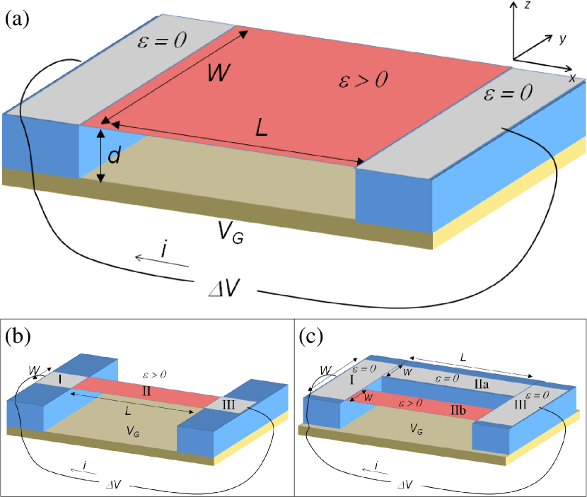
So far graphene NEMS have operated in the diffusive transport regime where electric Hone_2009 ; Singh_2010 transduction has been based on charge carrier density modulation. In those experiments the graphene was suspended above a backgate a distance as shown in Fig. 1(a). For a sheet of length and width the capacitance to the gate is Bolotin_2008 ; Andrei_2008 . Hence, the backgate voltage induces a carrier density . This leads to a conductivity of Adam_2008 , where is the mobility. Motion detection then uses the change in carrier density with distance. For a deflection away from the equilibrium distance , the relative change in conductance is Blanter_2010 . Note that only geometric length scales ( and ) enter into this expression.
A deflection also induces strain , which affects both the dynamical Atalaya_2008 ; Hone_2009 and the electronic Neto_RMP_2009 properties. For diffusive transport, strain leads to a linear increase in resistance Hong_2010 with a constant of proportionality of order unity. Hence, the relative change in conductivity due to strain, , is typically negligible compared to that from the carrier density modulation (for a more detailed anaysis, see Ref. Blanter_2010 ).
The situation is different if one considers coherent transport in graphene nanoribbons. The transverse confinement then give rise to conductance quantization. This prevents conductance changes due to motion in the backgate electrostatic field leaving strain as the only coupling between deformation and conductance. In this paper it is shown that in such graphene nanoribbon NEM-devices, an operating point where changes with displacement as can be found. For armchair nanoribbons [see fig. 1(b)], this is due to the opening of the transport gap. For zig-zag nanoribbons, which has no transport gap, an interferometer type set-up [see Fig. 1(c)] can be used. This set-up can also be used in the presence of edge-disorder.
Typically, graphene NEMS in equilibrium is not under zero strain. Not only will this inhibit ripple formation, it will also lead to more linear mechanical response. This strain can either be due built in strain or due to biasing to a working point . In the latter case, the sensitivity to a variation in deflection is naturally linear in , i.e. .
Transport through suspended graphene sheets and ribbons and in graphene with strained regions has been studied previously by several researchers Fogler_2008 ; Pereira_2009 ; Leon_2009 ; Mariani_2009 and the prospects of using strain in a controlled way to influence electronic properties is currently an active research field. Here the focus is on displacement detection in graphene nanoribbon NEMS.
The electronic properties close to the charge neutrality point are well described by the nearest neighbor tight binding model. Suppressing spin indices it is
| (1) |
Here is the creation operator for an electron at the point and the destruction operator for electrons at the site . The basis is here: , , , , and . For unstrained graphene, eV, and the Fermi velocity is .
For uniform strain along the direction (armchair edge) the bond-lengths change from to
while for uniform strain in the -direction (zig-zag edge),
Here is the Poisson ratio.
The changed lengths alter the hopping energies as . Typically, and it suffices to work to first order in . As , only first order terms in need to be kept. The spectrum then remains gapless and linear and can, for uniform strain, be described by the low energy Hamiltonian where
| (4) |
Here is a modified -matrix defined as
| (9) |
where
Hence, the Fermi velocity changes and becomes anisotropic, and the locations of the Fermi points in wavevector space changes.
The :s depend on the direction the strain is applied in and must be determined from first principles. In the context of carbon nanotubes, this has been studied extensively Kane_1997 ; Crespi_2000 ; Han_2000 mainly using tightbinding Hückel theory or Koster-Slater calculations Kleiner_2001 . More recently, density functional theory has been applied to strained graphene Yang_2008 ; Ribeiro_2009 . Here, the model of Ribeiro et al. Ribeiro_2009 will be used, where .
For strain along the direction (armchair) , Ribeiro_2009 , and to lowest order in , one finds
| (10) | |||||
| (11) |
Here are the conventional Pauli spin-1/2 matrices. For strain along the direction (zig-zag) and Ribeiro_2009 , which gives
| (12) | |||||
| (13) |
Consider now an armchair graphene nanoribbon of length , uniform width , suspended above a backgate as in Fig. 1(b). The supported parts (regions I and III) are assumed to be unstrained, while the suspended part (region II) is under finite strain . The conductance in the linear response regime is related to the transmission function as , where the prefactor 2 accounts for spin.
Confinement in the -direction leads to quantization of transverse wavevector components for integer . Here is given by Eq. (11). If the interfaces between strained and unstrained regions are along the -direction transverse mode number will be conserved. Hence, and the problem reduces to solving the 1D Dirac equation
| (14) |
Here is the effective potential in the ribbon and .
To calculate Eq. (14) should be solved in the regions I, II and III [see Fig. 1(b)] and the solutions matched at the interfaces (see also Ref. Peres2010_RMP, ). In a region of constant and , the solution with energy in band is
| (19) |
where and .
The matching of wavefunctions between regions is determined by current conservation Silin_1996 . The current-operator corresponding to the Hamiltonian in Eq. (14) is . Consequently, at the interface between regions I and II . However, the factors cancel in the final expression for
| (20) |
Here while are the propagation angles for electrons in regions I and II.
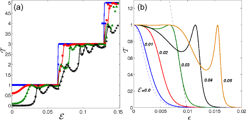
In Fig. 2 (a), is shown for strains as the solid lines. The discrete symbols, were obtained numerically using the tightbinding Hamiltonian in Eq. (1) and the relation . Here are the retarded (advanced) Green’s functions for the ribbon and are self energies accounting for semi-infinite graphene leads. Also, in the numerical calculation, no linearization in strain has been made. As can be seen, for the lowest plateau, a transport gap opens up with increasing strain.
From Eq. (20), the sensitivity of the conductance to ribbon displacements can be obtained. For the lowest transverse mode and for one finds
| (21) |
This dependence of on is shown in Fig. 2(b). Different curves correspond to different back-gate bias points, i.e. different values of . From this figure it is clear how for a given strain, one may chose a working point (by gating the structure) such that the slope of the -curve is maximal. This maximal slope, then defines the sensitivity.
The smallest sensitivity obtains for the working point at [dashed line in Fig. 2(b)]. A lower bound for the sensitivity can be found by setting in Eq. (21) and solving for the maximum magnitude of the slope. This gives . Hence, for a deflection of magnitude , the relative change in conductance is .
This result is valid for a metallic armchair ribbon where all edges are perfect and impurities absent. For transport restricted to the lowest transverse subband long range impurity scatterers will not affect the transport Wakabayashi_2009 . However, short range potentials will have effect. For armchair graphene nanoribbons both theory Blanter_2009 , and subsequent experiments Kim_2009 suggest that at low temperature, edge disorder induce localization. In this case, transport at low energies is goverend by variable range hopping and strongly supressed. Hence, schemes relying on a single armchair ribbon require nearly perfect edges.
Zig-zag nanoribbons are less sensitive to edge disorder. However, applying strain will not lead to a transport gap. Instead, to obtain a sensitivity of an interferometer with the suspended ribbon making up one of the arms [see Fig. 1(c)] can be used. In graphene ring-geometries Aharanov-Bohm oscillations have been observed at low temperatures Russo_2008 . Here, no external B-field is required. Instead, the effective gauge field due to the strain in the suspended arm is exploited.
The idea is again to use the lowest quantized conductance plateau. For zig-zag nanoribbons this is formed from current carried by the edge states. Hence, consider an edge-state coming from the unstrained region I, which split into the two arms IIa and IIb [see Fig. 1 (c)]. The state propagating in the strained arm (IIb) will aquire an extra phase [see Eq. (13)], and consequently one expects interference to modulate the conductance with a factor .
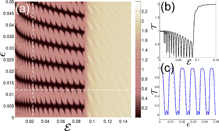
In Fig. 3(a) the result of numerically calculating (using the tight-binding Hamiltonian) from region I to region III as function of energy and strain is shown. Bright regions correspond to and dark regions to . These broad dark regions arise due to destructive interference. The fine structure is the result of backscattering at the interfaces where the ribbon split (inter-valley scattering). This is also visible in Fig. 3 (b) where the transmission for a specific strain % is shown as function of .
In Fig. 3(c) is shown for a fixed as function of strain (thick solid line). The period of the conductance oscillations agree well with the plotted function (thin black line). Hence, approximating yields, as was the case for the armchair ribbon, a sensitivity to deflections of .
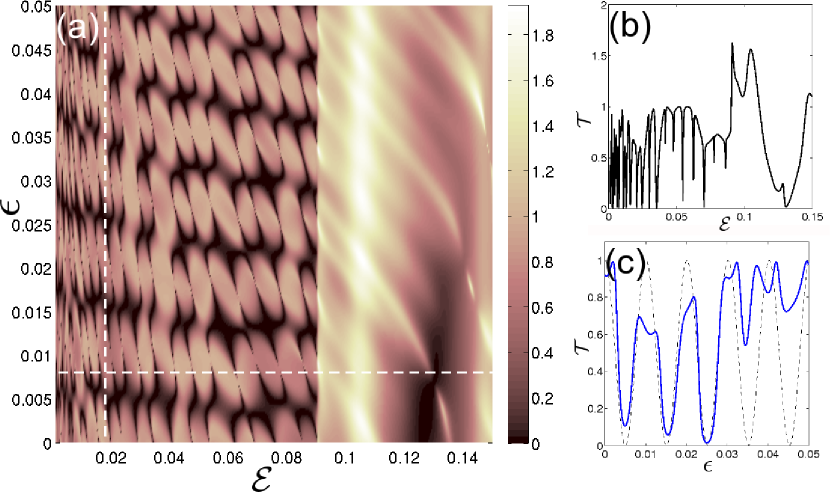
The effect of edge disorder on the interference pattern is shown in Fig. 4(a). Here, disorder has been accounted for by removing the outermost atoms with probability at random along each of the four zig-zag edges of the interferometer. Note that although as function of [panel (b)] is highly irregular, as function of strain [Fig. 4 (c)] show clear conductance modulations. Furthermore, comparing the solid line and the dashed line in Fig. 4 (c), it is clear that the the expression is still valid.
In conclusion, by exploiting the possibility to directly integrate coherent electron transport with graphene nanoribbon NEMS, the conductance through the structure can be made to depend on the mechanical deflection as . This is due to the strain induced shift of the Fermi-points (synthetic gauge field). It is this shift which causes the length scale to enter the expression for .
The author wishes to thank J. Kinaret, M. Jonson and M. Medvedyeva. This work has received funding from the Swedish Foundation for Strategic Research and the European Community’s Seventh Framework program (FP7/2007-2011) under grant agreement no: 233992.
References
- (1) J. S. Bunch, et al., Science 315, 490 (2007).
- (2) D. Garcia-Sanchez, et al., Nano Lett. 8, 1399 (2008).
- (3) J. T. Robinson, et al., Nano Lett., 8, 3441 (2008).
- (4) J. S. Bunch, et al., Nano Lett., 8, 2458 (2008).
- (5) C. Chen et al., Nat. Nanotechn. 4, 861-867 (2009).
- (6) V. Singh, et al., Nanotechn. 21, 165204 (2010).
- (7) C. Berger, et al., Science, 312, 1191 (2006).
- (8) H. B.Heersche, et al., Nature 446, 56 (2007).
- (9) M. Huefner, et al., New J. Phys. 12, 043054 (2010).
- (10) K. I. Bolotin et al., Sol. State. Comm. 146, 351 (2008).
- (11) X. Du, I. Skachko, A. Barker, and E. Y. Andrei, Nat. Nanotechn. 3, 491 (2008).
- (12) S. Adam and S. Das Sarma, Solid Stat. Comm. 146, 356 (2008).
- (13) M. Medvedyeva, and Ya. M. Blanter, arXiv:1006.5010 (2010).
- (14) J. Atalaya, A. Isacsson, and J. M. Kinaret, Nano. Lett. 8 (2008).
- (15) A. H. Castro Neto, et al., Rev. Mod. Phys. 81, 109 (2009).
- (16) Y. Lee,et al., Nano Lett. 10, 490 (2010).
- (17) M. M. Fogler, F. Guinea, and M. I. Katsnelson, Phys. Rev. Lett. 101, 226804 (2008).
- (18) V. M. Pereira, and A. H. Castro Neto, Phys. Rev. Lett. 103, 046801 (2009).
- (19) E. Prada et al., Phys. Rev. B 81, 161402(R) (2010).
- (20) F. von Oppen, F. Guinea, and E. Mariani, Phys. Rev. B 80, 075420 (2009).
- (21) C. L. Kane, and E. J. Mele, Phys. Rev. Lett. 78, 1932 (1997).
- (22) P. E. Lammert and V. H. Crespi, Phys. Rev. B 61, 7308 (2000).
- (23) L. Yang, and J. Han, Phys. Rev. Lett. 85, 154 (2000).
- (24) A. Kleiner, and S. Eggert, Phys. Rev B. 63, 073408 (2001).
- (25) L. Sun, et al., J. Chem. Phys. 129, 074704 (2008).
- (26) R. M. Ribeiro, et al., New J. Phys. 11, 115002 (2009).
- (27) N. M. R. Peres, Rev. Mod. Phys. 82 (2010).
- (28) A. V. Kolesnikov and A. P. Silin, Zh. Eksp. Teor. Fiz. 109 2125 (1996) [JETP, 82 (6), 1146 (1996)].
- (29) M. Yamamoto, Y. Takane, and K. Wakabayashi, Phys. Rev. B 79 125421 (2009).
- (30) I. Martin and Ya. M. Blanter, Phys. Rev. B 79, 235132 (2009).
- (31) M. Y. Han, J. C. Brant, and P. Kim, Phys. Rev. Lett. 104, 056801 (2010).
- (32) S. Russo, et al., Phys. Rev. B. 77, 085413 (2008).