∎
Network for Computational Nanotechnology
Purdue University, West Lafayette, USA 47907
Tel.: 1-765-40-43589 22email: abhijeet.rama@gmail.com
Modified valence force field approach for phonon dispersion: from zinc-blende bulk to nanowires
Abstract
The correct estimation of thermal properties of ultra-scaled CMOS and thermoelectric semiconductor devices demands for accurate phonon modeling in such structures. This work provides a detailed description of the modified valence force field (MVFF) method to obtain the phonon dispersion in zinc-blende semiconductors. The model is extended from bulk to nanowires after incorporating proper boundary conditions. The computational demands by the phonon calculation increase rapidly as the wire cross-section size increases. It is shown that the nanowire phonon spectrum differ considerably from the bulk dispersions. This manifests itself in the form of different physical and thermal properties in these wires. We believe that this model and approach will prove beneficial in the understanding of the lattice dynamics in the next generation ultra-scaled semiconductor devices.
Keywords:
Dynamical matrix Nanowire Phonons Valence Force Fieldpacs:
63.20.-e Phonons in crystal lattices 63.22.Gh Nanotubes and nanowires1 Introduction
The lattice vibration modes known as ‘phonons’ determine many important properties in semiconductors like, (i) the phonon limited low field carrier mobility in mosFETs JAP_anantram ; buin_sinw_phonon , (ii) the lattice thermal conductivity in semiconductors which plays an important role in thermoelectric design Mingo_kappa ; mingo_ph ; thermal_cond_dim , and (iii) the structural stability of ultra-thin semiconductor nanowires SINW_110_phonon . A physics-based method to calculate the phonon dispersion in semiconductors is required to understand and link all these issues. As the device size approach the nanometer scale and as the number of atoms in the structure become countably finite, a continuum material description is no longer accurate. This work provides a complete and elaborate description of an atomistic phonon calculation method based on ‘Valence Force Field’ (VFF) model Keating_VFF ; VFF_mod_herman ; VFF_mod_zunger , a frozen phonon approach, with application to bulk and nanowire structures.
A variety of methods have been reported in the literature for the calculation of the phonon spectrum such as the Valence Force Field (VFF) method and its variants VFF_mod_herman ; VFF_mod_zunger ; Keating_VFF ; McMurry_VFF , Bond Charge Model (BCM) bcm_weber ; BCM_model , Density Functional Method SINW_110_phonon ; jauho_method , etc. We focus on VFF methods in this work. There are multiple reasons for using a VFF based model: (a) in covalent bonded crystals, like Si, Ge, GaAs, simple VFF potentials are sufficient to match the experimental data McMurry_VFF , (b) valence coordinates and hence the potential energy (U) depend only on the relative positions of the atoms and are independent of rigid translations and rotations of the solid, and (c) it is easy to extend the model to confined ultra-scaled structures made of few atoms since the interactions are at the atomic level.
The original Keating VFF model Keating_VFF describe the LA, LO and TO phonons reasonably well in zinc-blende materials, however, it does not produce the flatness in the TA branch in Si, Ge bcm_weber ; VFF_mod_herman . Also the limitation of the model to correctly describe the elastic constants (C11, C12, C44) in these materials also limits its use VFF_mod_herman . In order to extend the available VFF models to nanostructures, we need to identify the models which can correctly describe the phonons in the entire Brillouin zone (BZ) in zinc-blende semiconductors. There are older works where as many as six parameters six_param_VFF have been used in VFF to obtain the correct phonon dispersions. However, the task of this work has been to obtain a VFF model which (i) can capture the correct physics and (ii) is computationally not very expensive. Hence such a model can be extended to nanostructures like nanowires, ultra-thin-bodies, etc. To this end we have identified two VFF models which satisy the requirements. The modified VFF (MVFF) model presented here combines these two following models, (i) VFF model from Sui et. al VFF_mod_herman which is suitable for non-polar materials like Si and Ge and (ii) VFF model from Zunger et. al VFF_mod_zunger which is suitable for treating polar materials like GaP, GaAs, etc. This extended model is called the ‘MVFF model’ in this study.
The main focus of this work is to show the implementation of VFF models for phonon calculation in zinc-blende (diamond) lattices. We present the details on the atomic groups which make up the interactions, the application of boundary conditions in the nanostructures, the eigen value problem, the computational requirements and the evaluation of lattice properties. We benchmarked the model for variety of zinc-blende materials like Si, Ge, GaP, GaAs, etc. In this paper we present the results using Si (sometimes Ge too) as a specific example. We also present a comparison of the Keating VFF model Keating_VFF with the present MVFF model for Si to elucidate the differences in physical results and their computational requirements.
Previous theoretical works have reported the calculation of phonon dispersions in SiNWs using a continuum elastic model and Boltzmann transport equation continuum_model , atomistic first principle methods like DFPT (Density Functional Perturbation Theory) SINW_110_phonon ; jauho_method ; sinw_cv ; strain_effect_1 and atomistic frozen phonon approaches like Keating-VFF (KVFF) Mingo_kappa ; SINW_111 . Thermal conductivity in SiNWs has been studied previously using the KVFF model mingo_ph ; strain_effect_2 .
This paper has been arranged in the following sections. The MVFF theory (a ‘frozen phonon’ method) for the phonon dispersion in zinc-blende semiconductors is reviewed in Sec. 2. It provides details about the total potential energy (U) of the crystals in the MVFF model (Sec. 2.1), construction of the dynamical matrix (DM) (Sec. 2.2), application of boundary conditions to the DM (Sec. 2.3), solution of the resulting eigen value problem (Sec. 2.4), and calculation of sound velocity () (Sec. 2.5), lattice thermal conductance () (Sec. 2.6) and the mode Grneisen parameters (Sec. 2.7) using the phonon spectrum. The computational details for the calculation of phonon dispersion are presented in Sec. 3. Different aspects of the dynamical matrix like the size, fill-factor, sparsity pattern, etc., are provided in Sec. 3.1. Timing analysis for the assembly of the DM are shown in Sec.3.2. Section 4 presents, a benchmark of the MVFF results against experimental data for different semiconductors (Sec. 4.1), a comparison of the MVFF and Keating-VFF (KVFF) models (Sec.4.2), phonon spectrum in Si nanowires (SiNW) with free and clamped boundary conditions (Sec. 4.3) and lattice thermal conductance using SiNW phonon spectrum (Sec.4.4). Conclusions are given in Sec.5.
2 Theory, Approach and Parameters
In a given system, the phonons are modeled by solving the equations of motion of its atomic vibrations. Since VFF is a crystalline model, the dynamical equation for each atom ‘i’ can be written as,
| (1) |
where, , and U are the vibration vector of atom ‘i’, the total force on atom ‘i’ in the crystal, and the potential energy of the crystal, respectively. Equation (1) indicates that the calculation of the vibrational frequencies requires a good estimation of the potential energy of the system. The next part discusses the calculation of U within the MVFF model.
2.1 Crystal Potential Energy (U)
The MVFF method VFF_mod_herman ; VFF_mod_zunger ; Keating_VFF approximates the potential energy U, for a zinc-blende (or diamond) crystal, based on the nearby atomic interactions (short-range) VFF_mod_herman ; VFF_mod_zunger as,
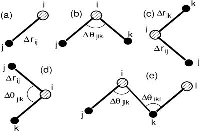
| (2) | |||||
where , , and represent the total number of atoms in one unitcell, the number of nearest neighbors for atom ‘i’, and the coplanar atom groups for atom ‘i’, respectively. The first two terms in Eq. (2) are from the original KVFF model Keating_VFF . The other interaction terms are needed to accurately describe the phonon dispersion in the entire Brillioun Zone (BZ). The terms and represent the elastic energy from bond stretching and bond-bending between the atoms connected to each other (Fig. 1.a,b). The terms , and represent the cross bond stretching VFF_mod_herman ; VFF_mod_zunger , cross bond bending-stretching VFF_mod_zunger , and coplanar bond bending VFF_mod_herman interactions, respectively (Fig. 1. c,d,e). The functional dependence of each interaction term on the atomic positions is given by,
| (3) | |||||
| (4) | |||||
| (5) | |||||
| (6) | |||||
| (7) |
where , is the angle deviation of the bond between atom ‘i’ and ’j’ and bond between atom ‘i’ and ‘k’. The term () is the non-ideal (ideal) bond vector from atom ‘i’ to ‘j’. The coefficients , , , , and determine the strength of the interactions used in the MVFF model (like spring constants). They are used as fitting parameters to reproduce the bulk phonon dispersion VFF_mod_herman ; VFF_mod_zunger . The unit of these fitting parameters are in force per unit length (like ). The value of these strength parameters also changes according to the deviation of the bond length and bond angle from their ideal values. This enables the inclusion of the anharmonic properties of the lattice vibrations anharmonic in this model. Hence, MVFF is sometimes referred to as ‘quasi-anharmonic’ model.
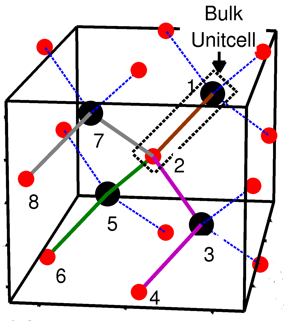
Interaction Terms: The primitive bulk unitcell used for phonon calculation is made of two atoms (anion-cation pair for zinc-blende and 2 similar atoms for diamond). The black dotted box with atom 1 and 2 represents the bulk primitive unitcell in Fig. 2. The total number of terms in each interaction in Eq. (3-7) for a bulk unitcell are provided in Table 1. Apart from the coplanar bond bending interaction VFF_mod_herman all the other terms involve nearest neighbor interactions . There are 21 coplanar (COP) groups present in a bulk zinc-blende unitcell which are needed for the calculation of the phonon dispersion. For clarity some of these COP groups shown using the number combinations in the caption of Fig. 2. Each group consists of 4 atom arranged as anion(A)-cation(C)-anion(A)-cation(C) (eg. 1(A)-2(C)-3(A)-4(C) in Fig. 2). Details about the coplanar interaction groups are provided in Appendix A.
| Interaction Type | Total terms (anion+cation) |
|---|---|
| Bond stretching (bs) | 8 |
| Bond bending (bb) | 12 |
| Cross bond stretching (bs-bs) | 12 |
| Cross bond stretch-bend (bs-bb) | 12 |
| Coplanar bond bending (bb-bb) | 21 |
2.2 Dynamical Matrix (DM)
The dynamical matrix captures the motion of the atoms under small restoring force in a given system. In this Section we discuss the structure of this matrix. The derivation of the DM from the equation of motion is given in Appendix B. The DM calculation is based on the harmonic approximation (see Appendix B). For the interaction between two atoms ‘i’ and ‘j’, the DM component at atom ‘i’ is given by,
| (8) |
The 9 components of are defined as,
where is the total number of atoms in the unitcell. For each atom the size of is fixed to 3 3. For atoms in the unitcell the size of the dynamical matrix is . However, the matrix is mostly sparse. The sparsity pattern, fill factor, and other related properties of the DM are discussed in Section 3.
Symmetry considerations in the DM: Under the harmonic approximation the dynamical matrix exhibit symmetry properties that can be readily utilized to reduce its assembly time. From software development point of view this is crucial in optimizing matrix construction time, storage and compute times. Due to the continuous nature of the potential energy U, we have,
| (10) |
A closer look at Eq. (10) shows the following symmetry relation,
| (11) |
This reduces the total number of calculations required to construct the dynamical matrix and speeds up the calculations. Also if the matrix is stored for repetitive use, then only one of the symmetry blocks needs to be stored. This reduces the memory requirement in the software by a factor of 2. Further reduction in the construction time of DM can be achieved depending on the type of interaction, the symmetry of the crystal, and some implementation tricks (not covered in this work, see Ref.DM_element_reduction for more discussion). Also the knowledge about the underlying symmetry of the matrix can also help in the selection of linear algebra approaches which can reduce the final solution time (not covered in this work).
| Dimensionality | Periodic BC | Finite Edge BC |
|---|---|---|
| Bulk (3D) | 3 | 0 |
| Thin Film (2D) | 2 | 1 |
| Wire (1D) | 1 | 2 |
| Quantum Dot (0D) | 0 | 3 |
2.3 Boundary conditions (BC)
To calculate the eigenmodes of the lattice vibration, it is important to apply appropriate boundary conditions to the DM. In the case of bulk material, the unitcell has periodic (Born-Von Karman) boundary conditions along all the directions (x,y,z) VFF_mod_herman ; bcm_weber since the material is assumed to have infinite extent in each direction. However, for nanostructures the boundary conditions are different due to the finite extent of the material along certain directions. The boundary conditions vary depending on the dimensionality of the structure (1D, 2D or 3D, see Table 2) for which the dynamical matrix is constructed. There are 2 types of boundary conditions; (i) Periodic Boundary condition (PBC) which assumes infinite material extent in a particular direction and (ii) Finite Edge boundary conditions (FEBC) such as open or clamped, which assumes finite material extent in a particular direction. Table 2 provides the boundary condition details depending on the dimensionality of the structure used for phonon calculation.
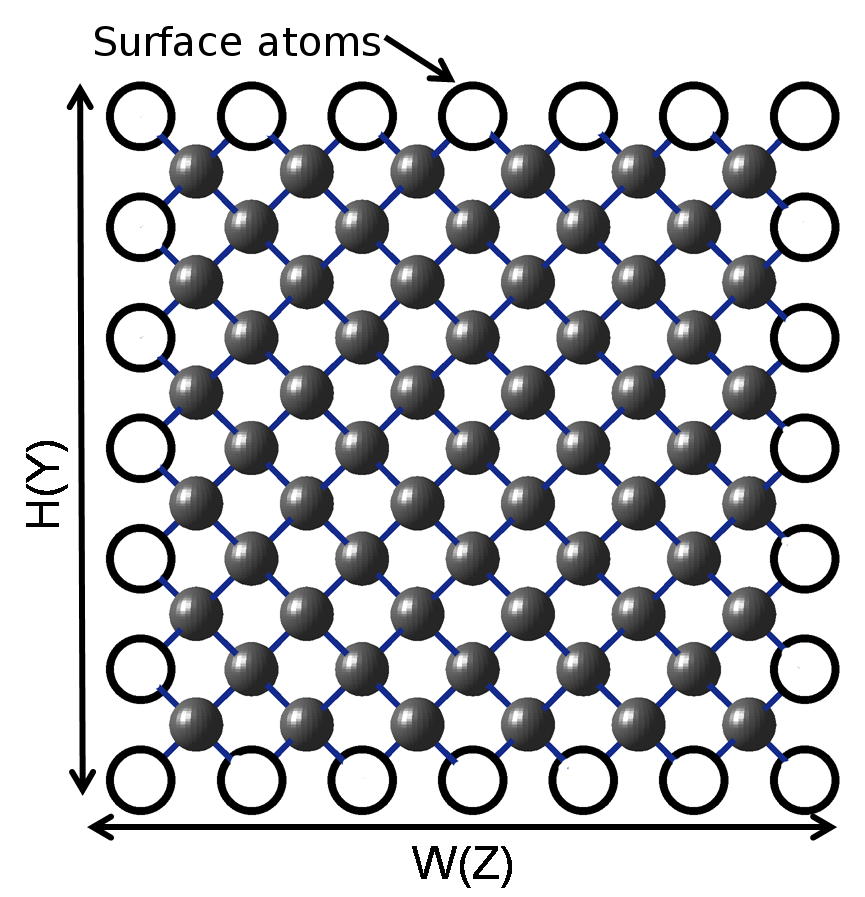
The use of PBC has been discussed in many papers like VFF_mod_herman ; VFF_mod_zunger ; bcm_weber . In this work we consider the boundary conditions associated with geometrically confined nanostructures. The vibrations of the surface atoms can vary from completely free (free BC) to damped oscillations (damped BC). It is shown next that all these cases can be handled within one single boundary condition.
Boundary conditions for nanostructures: The surface atoms (Fig. 3, hollow atoms) of the nanostructures can vibrate in a very different manner compared to the inner atoms (Fig. 3, filled atoms) since the surface atoms have different number of neighbors and ambient environment compared to the inner atoms. The degree of freedom of the surface atoms can be represented by a direction dependent damping matrix , defined in Appendix C. In such a case the dynamical matrix component between atom ‘i’ and ‘j’ () is modified to,
| (12) |
2.4 Diagonalization of the dynamical matrix
After setting up the dynamical matrix with appropriate BCs the following eigen-value problem must be solved,
| (13) |
where, M is the atomic mass matrix. and are the phonon polarization and momentum vector respectively. The term is a column vector containing all the phonon eigen displacement modes associated with the polarization and momentum . For simplified numerical calculation slightly modifying Eq. (13) leads to,
| (14) |
The detail for obtaining is outlined in Appendix D. To obtain Eq. (14) another step is needed. The time dependent vibration of each atom () are represented as the linear combination of phonon eigen modes of vibration (a complete basis set) as,
2.5 Sound Velocity ()
A wealth of information can be extracted from the phonon spectrum of solids. One important parameter is the group velocity () of the acoustic branches of the phonon dispersion which gives the velocity of sound () in the solid. Depending on the acoustic phonon branch used for the calculation of , the sound velocity can be either, (a) longitudinal () or (b) transverse (). In solids, is obtained near the BZ center (for q ) where . Thus, is given by,
| (17) |
where is the either the transverse or longitudinal polarization of the phonon frequency.
2.6 Thermal Conductance ()
Another important physical property of the semiconductors that can be extracted from the phonon spectrum is the lattice thermal conductivity. For a small temperature gradient () at the two ends of a semiconductor, the is obtained using Landauer approach Land as outlined in Refs. Mingo_kappa ; mingo_ph ; jauho_method . For 1D nanowires at a temperature ‘T’ is given by mingo_ph ; Wallace ,
| (18) |
where is the transmission of a phonon branch at frequency , and , the reduced Planck’s constant and Boltzmann constants, respectively. Equation (18) is of general validity and involves a low temperature approximation. Scattering causes the conductance to vary with the nanowire’s length (L). In the case of ballistic thermal transport the transmission () is always 1 for all the eigen frequencies.
2.7 Mode Grneisen Parameter ()
One of the advantages of using the MVFF model is its ability to keep track of the phonon frequency shift under crystal stress. Under the action of hydrostatic strain the crystal is compressed without changing its symmetry. With pressure (P) the phonon frequency shifts, which is measured by a unitless parameter called the mode ‘Grneisen Parameter’ given as
| (19) | |||||
| (20) |
where, is the eigen frequency for the ith branch at momentum point. The terms B, P and V are the volume compressibility factor, pressure on the system, and volume of the crystal, respectively. Theoretically this parameter is extracted by calculating the eigen frequencies at ambient condition (P = 0) and at small hydrostatic pressure () and then taking the difference in the calculated frequencies. The modification of the force constants under hydrostatic pressure is outlined in Ref. VFF_mod_herman . The value of this parameter at high symmetry points (, X, etc.) in the BZ can be measured experimentally by Raman scattering spectroscopy gparam_1 .
In the remaining Sections we provide the computational details, show results on phonon dispersion in bulk and nanowires and give some results on , and ballistic in semiconductor nanowires.
3 Computational Details
This Section provides the computational details involved in obtaining the phonon dispersion in semiconductor structures. Details about bulk and nanowire (NW) structures are provided.
3.1 Dynamical matrix details
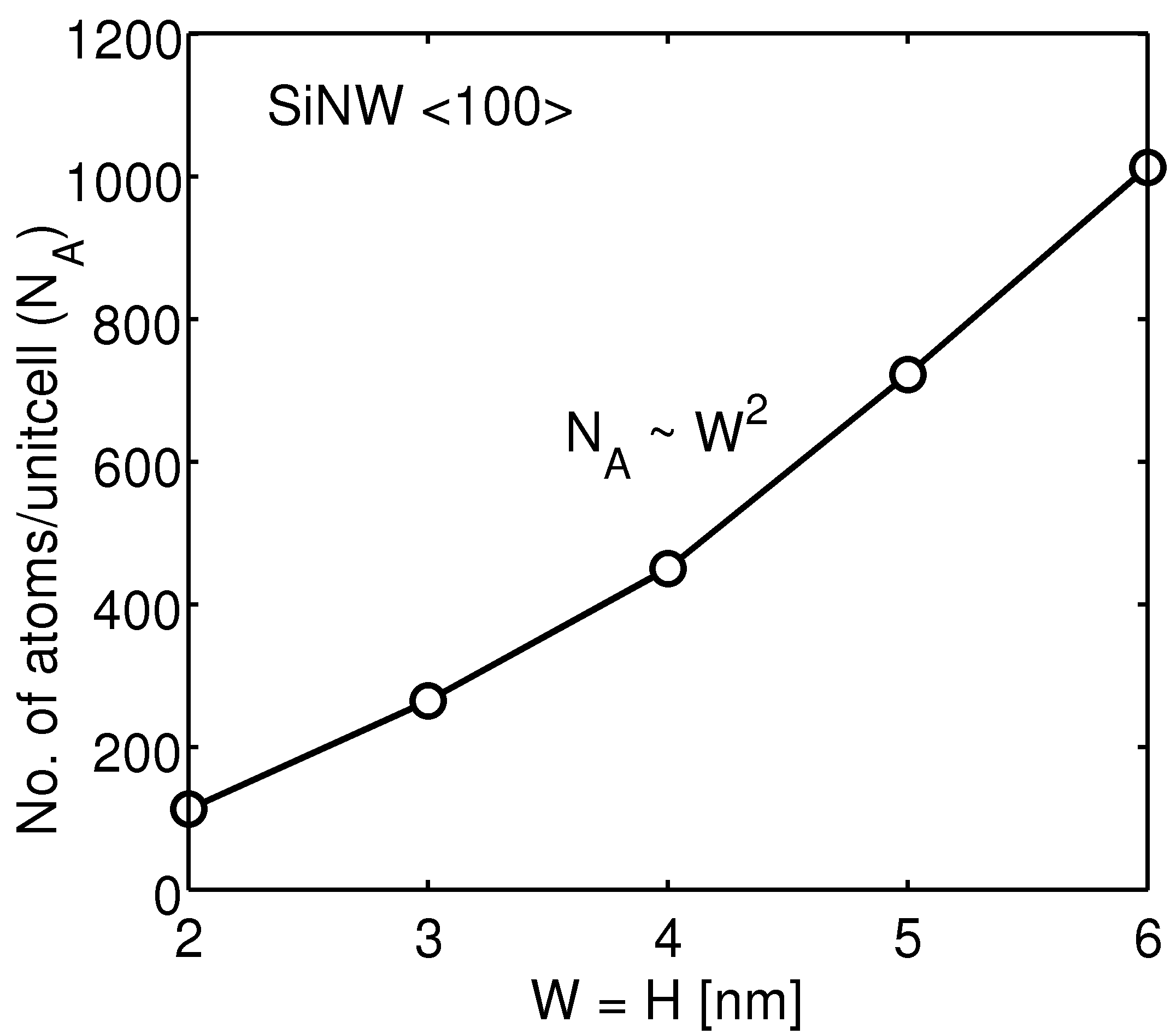
A primitive bulk zinc-blende unitcell has 2 atoms. This fixes the size of the DM for the bulk structure to 6 6 () (see Sec.2.2). However, for the case of nanowires, varies with shape, size and orientation of the wire jauho_method . In this paper, all the results are for square shaped SiNW with 100 orientation. Figure 4 shows the variation in with the width (W) of Silicon NW (SiNW). The number of atoms increase quadratically with W. For a 6nm 6nm SiNW, is 1013 which means the size of DM is 3,039 3,039. Extrapolating the data gives around 7,128 atoms for a 16nm 16nm SiNW resulting in a DM of size 21,384 21,384 (details in Appendix E). So, the dynamical matrix size increases rapidly with increase in width.
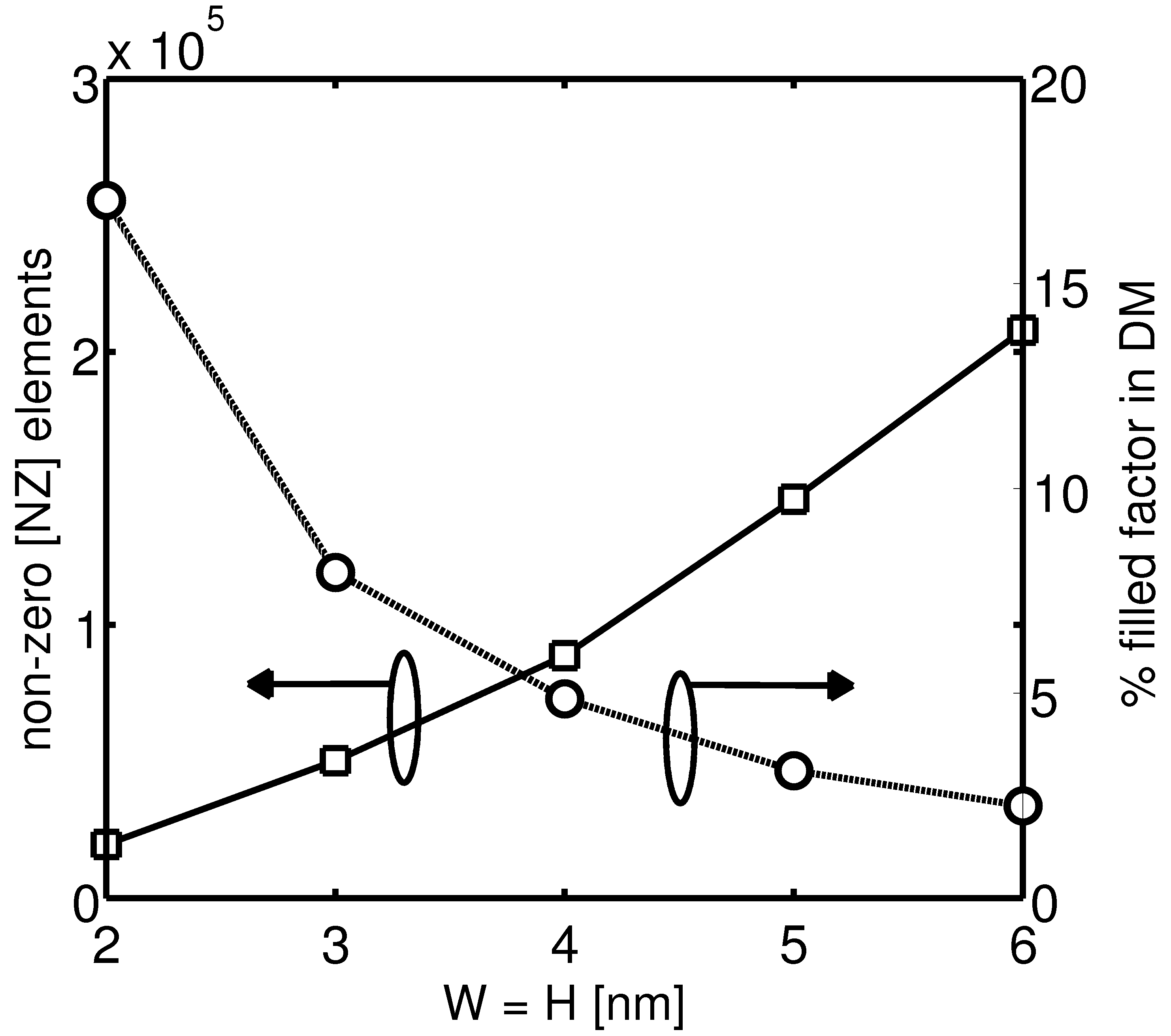
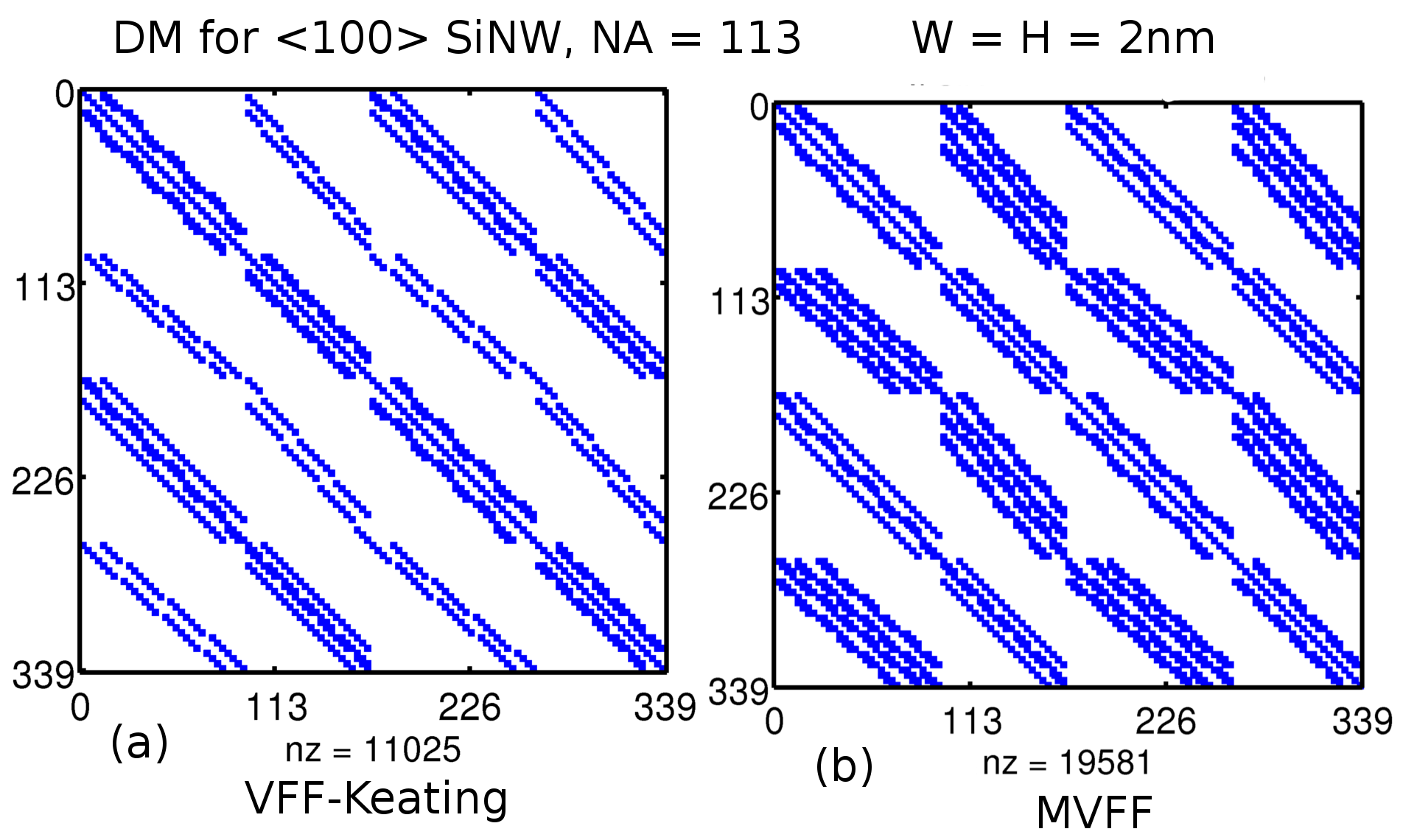
The increase of the DM size with wire cross-section imposes constraint on the structure size which can be solved using the atomistic MVFF method. However, the entire matrix is quite sparse which can be utilized significantly to expand the physical size of the system that can be simulated by using compressed matrix storage methods. The qualitative idea about the filling can be observed from the sparsity pattern for a 2nm 2nm SiNW dynamical matrix as shown in Fig. 5. The quantitative analysis of the fill fraction of the DM and the number of non-zero elements (NZ) in the DM are shown in Fig. 6. The non-zero elements in the DM increase quadratically with W of SiNW. An estimate for 16nm 16nm SiNW gives about 800,117 non-zero elements (details in Appendix E). However, to get an idea about the absolute filling of the DM we define a term called the ‘fill-factor’ given as,
Thus, fill factor varies inversely with number of atoms in the unitcell. The relation of NZ with NA is provided in Appendix E.
The percentage fill factor of the DM reduces with increasing W of SiNW (Fig. 6). This value is 0.1% for a SiNW with W 25nm (Appendix E) . So even though the non-zero elements increase with W, DM becomes sparser which allows to store the DM in special compressed format like compressed row/column scheme (CRS/CCS) CRS_CCS enabling better memory utilization.
| W | NZ | % fill | per k | ||
| (nm) | factor | (sec) | (hours) | ||
| 16 | 7128 | 800117 | 0.423 | 238.48 | 33.2 |
| 20 | 11120 | 1252490 | 0.224 | 370.73 | 129.5 |
| 25 | 17346 | 1.96 | 0.101 | 576.91 | 505.2 |
| ∗Time estimates on an Intel T6400, 2GHz processor. | |||||
3.2 Timing analysis for the computation of DM
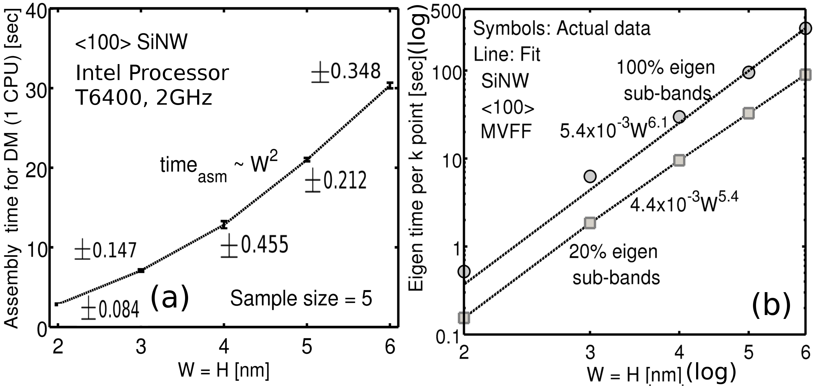
The numerical assembly of the DM takes a considerable time due to the many interactions calculated in the MVFF model. The assembly time () increases as increases. To give an idea about the timing, the dynamical matrix for SiNW with different W are constructed on a single CPU (Intel T6400, 2GHz processor). The assembly time is calculated for each width 5 times to obtain a mean value for the . The error bar at each W is the standard deviation from the mean (Fig. 7a). In the present case the assembly of the DM is done atom by atom which is useful for distorted materials as well as alloys. The assembly time for the DM in single materials can be reduced dramatically by the assumption of homogeneous bond lengths and a matrix stamping technique nemo3d .
After the DM is assembled, it is solved to obtain the eigen modes of oscillations. The time needed to diagonalize () the DM, for each ‘k’ point, using the MATLAB ‘eig’ function eig_matlab is also calculated (on the same processor). The value varies as the sixth power of W as shown in Fig. 7b. However, if only 20% percent of the Eigen values are calculated the time requirement now goes by the fifth power (shown by the lower line in Fig. 7b). The Eigen values in this case are calculated using the ‘eigs’ function in matlab eigs_method. The calculation of only 20% of the Eigen spectrum reduces the per-k energy calculation time by 75% for a square SiNW with W = H = 6nm. However, the possibility of using only the partial spectrum for the evaluation of the important lattice parameters (like thermal conductance, etc.) is not in the scope of present discussion. For the calculation of physical quantities, in this paper, the complete Eigen spectrum has been used.
Extrapolating the data for the computational and timing requirement obtained for the smaller SiNWs, can provide some estimates about the size and time requirement for larger SiNWs (Table 3). Analytical fits for the variation of the size and time parameters with W are provided in Appendix E. The timing requirements also help us in the resource requirement estimate for a future Bandstructure Lab extension for phonons on nanoHUB.org bslab .
| Material | Model | |||||
|---|---|---|---|---|---|---|
| Si | MVFF VFF_mod_herman | 45.1 | 4.89 | 1.36 | 0 | 9.14 |
| Si | KVFF Keating_VFF | 48.5 | 13.8 | 0 | 0 | 0 |
| Ge | MVFF VFF_mod_herman | 37.8 | 4.24 | 0.49 | 0 | 7.62 |
4 Results
In this Section we show results for the phonon spectrum in bulk and confined semiconductor structures using both the MVFF and KVFF models. Also some of the physical properties extracted from the phonon dispersions are reported.
4.1 Experimental Benchmarking
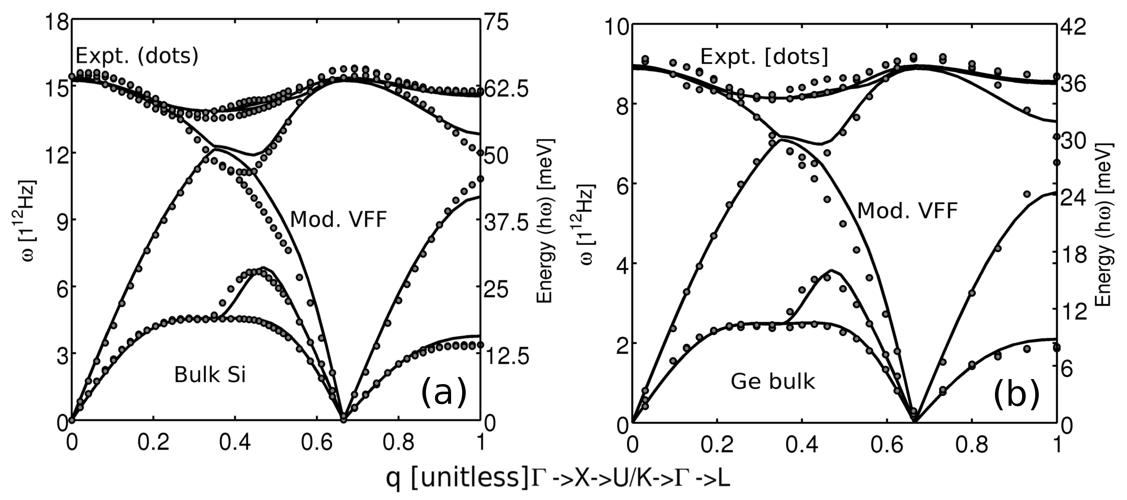
The first step to check the correctness of the MVFF model is to compare the simulated results with experimental data. Figure 8 shows the simulated and experimental bulk_si_exp_phon bulk phonon dispersion for (a) Silicon and (b) Germanium. The value of the strength parameters are provided in Table 4. A very good agreement between the experimental and simulated data is obtained. To further support the correctness of the MVFF model, is calculated in bulk Si and Ge along 100 direction (Table 5). The extracted sound velocity compares very well with the experimental sound velocity data ioffe_online (max error 10%).
| Material | Structure | calc. | Expt. ioffe_online |
|---|---|---|---|
| Si | Bulk [100] | 9.09 | 8.43 (8%) |
| Bulk [100] | 5.71 | 5.84 (2%) | |
| NW | 6.51 | – | |
| NW | 4.46 | – | |
| Ge | Bulk [100] | 5.13 | 4.87 (5%) |
| Bulk [100] | 3.36 | 3.57 (6%) | |
| NW | 3.70 | – | |
| NW | 2.61 | – |
The comparison of second order elastic constants for Si and Ge evaluated using the MVFF model (using the formulation provided in Ref. VFF_mod_herman ) with experimental data Madelung is provided in Table 6. The MVFF derived values compare quite well with the experimental data Madelung .
Another comparison carried out to test the robustness of MVFF model is the comparison of the mode Grneisen parameters at the high symmetry and X point with the experimental data (see Table 7). The MVFF results are in good comparison with the experimental data.
An advantage of using a higher order phonon model is that both phonon dispersions as well the physical parameters can be matched to a good accuracy. Hence, MVFF model captures the experimental phonon dispersion as well as the elastic properties in bulk zinc-blende material very well.
| Material | Model | C11 | C12 | C44 |
|---|---|---|---|---|
| Si | MVFF | 16.80 | 6.47 | 7.63 |
| Si | Expt. | 16.57 | 6.39 | 7.96 |
| Error | 1.4% | 1.2% | 4.14% | |
| Ge | MVFF | 13.22 | 4.84 | 6.29 |
| Ge | Expt. | 12.40 | 4.13 | 6.83 |
| Error | 6.6% | 17.2% | 8% |
4.2 Comparison of VFF models
In this Section we compare the original Keating VFF model Keating_VFF with the MVFF model to show the need for the more elaborate MVFF model. Both computational requirement and the physical result comparisons are provided in this Section. From computational point of view the DM for both the models are quite different (Fig. 5). The difference in the sparsity pattern arises because of the coplanar interaction present in the MVFF model which takes into account interactions beyond the nearest neighbors. The KVFF model has fewer non-zero elements compared to the MVFF model. The increase in number of NZ elements increases more rapidly in the MVFF model vs. the KVFF model (Fig. 9). The MVFF model required twice as many matrix elements compared to the KVFF model for a 5nm 5nm SiNW. Thus, MVFF model demands more storage space.
| MVFF | KVFF | Expt./Abinitio | Ref. | |
|---|---|---|---|---|
| 1.05 | 0.81 | gparam_1 | ||
| -0.68 | -0.43 | -0.62 | VFF_mod_herman | |
| 0.95 | 0.7 | 0.85 | VFF_mod_herman | |
| 1.08 | 0.816 | 1.03 | gparam_2 | |
| 1.25 | 0.83 | gparam_1 | ||
| -1.58 | -0.33 | gparam_1 |
A comparison of the bulk Si phonon dispersion from the two models is shown in Fig. 10. The parameters for both the models are provided in Table 4. Qualitatively MVFF shows a better match to the experimental data compared to the KVFF model. There are few important points to be noted in the bulk phonon dispersion. The KVFF model reproduces the acoustic branches very well near the Brillouin zone (BZ) center but overestimates the values near the zone edge (at X and L point in the BZ, Fig. 10). The MVFF model overcomes this shortcoming and reproduces the acoustic branches very well in the entire BZ. Comparison of sound velocity along the 100 direction for bulk Si obtained from both the models show a very good match to the experimental data (Table 8).

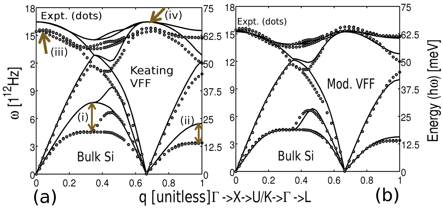
The KVFF model overestimates the optical phonon branch frequencies whereas the MVFF model produces a very good match to the experimental data (Fig. 10) and Table 8. The comparison of the optical frequency at the point reveals that the KVFF model overshoots the experimental value by 7% whereas the MVFF model is higher by only 0.6%.
The comparison of the mode Grneisen parameters for bulk Si using the two models is shown in Table 7. KVFF gives wrong values of these parameters compared to the experimental values. However, MVFF model is able to reproduce the experimental value very well. This shows the importance of using a quasi-harmonic model to correctly obtain the phonon frequency shifts VFF_mod_herman ; gparam_3 . A similar failure of the KVFF model for III-V zinc-blende materials have been reported in Ref. olga_gparam .
The correct representation of bulk phonons is very important since this will affect the phonon spectrum of the confined structures. At the same time the physical properties like lattice thermal conductivity, phonon density of states (DOS), etc. are also affected. Since the MVFF model matches the experimental bulk phonon data more accurately, though at the expense of additional calculations and storage, compared to the original KVFF model, we believe that the MVFF model will give better results for phonon dispersion in nanostructures.
4.3 Phonons in nanowires
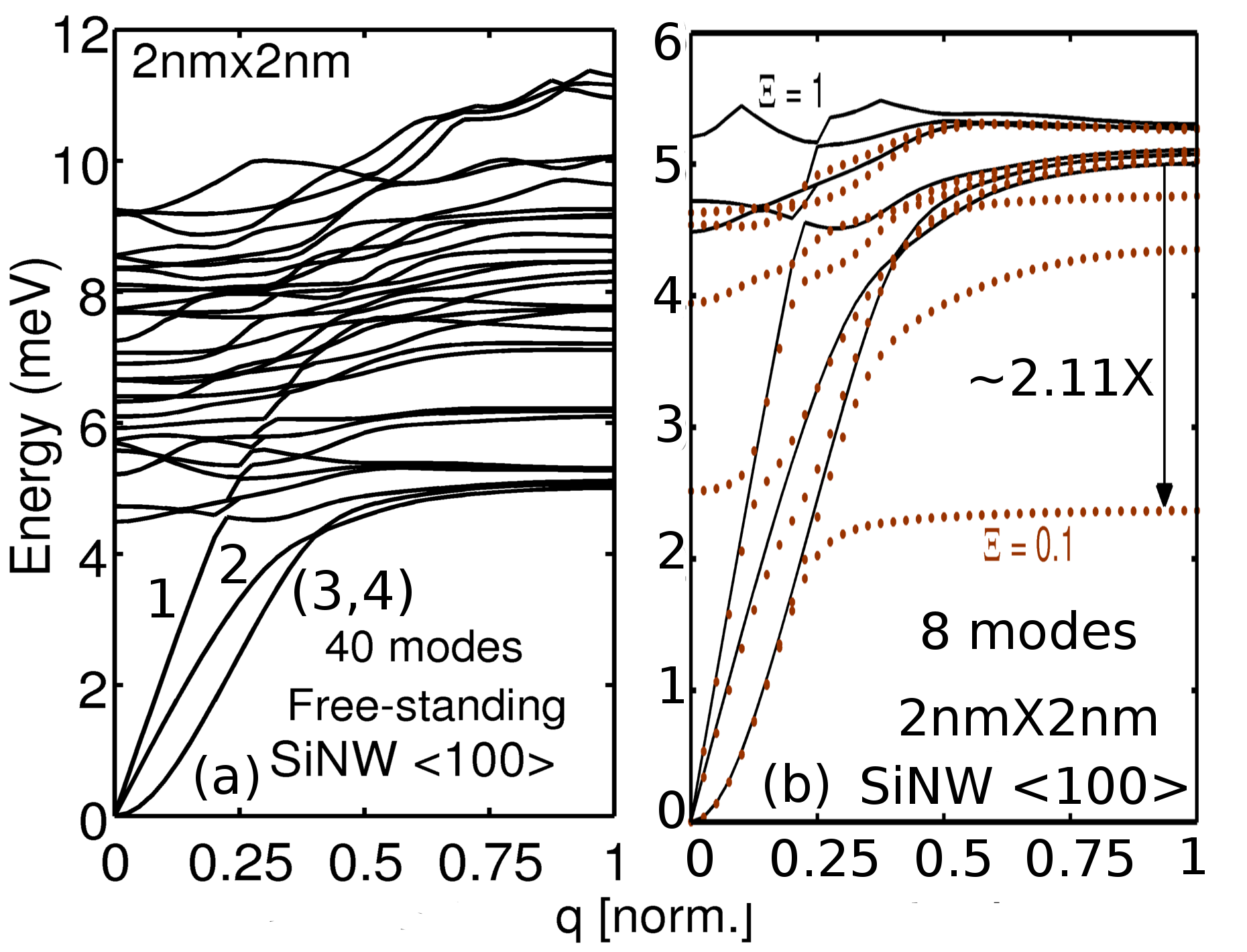
After benchmarking the bulk phonon dispersion, the same parameters are used to obtain the phonon spectrum in 100 square SiNW (Fig. 11). The result for a 2nm 2nm free-standing SiNW is shown in Fig. 11(a). Some of the key features to notice in the phonon dispersion are, (i) presence of two acoustic branches ( q, 1,2 in 11(a)), (ii) two degenerate modes (3,4 in 11(a)) with , which are called the ‘flexural modes’, typically observed in free-standing nanowires SINW_110_phonon ; jauho_method ; SINW_111 and (iii) heavy mixing of the higher energy sub-bands leaving no ‘proper’ optical mode. The features are quite different from the bulk phonon spectrum. This will strongly affect other physical properties of nanowires extracted using the phonon dispersion.
| Model | |||
|---|---|---|---|
| (km/sec) | (km/sec) | (THz) | |
| MVFF | 9.09 | 5.71 | 15.49 |
| KVFF | 8.35 | 5.75 | 16.46 |
| Expt. | 8.43 ioffe_online | 5.84 ioffe_online | 15.39 bulk_si_exp_phon |
In Fig. 11b, we explore the effect of a substrate on which the nanowire may be mounted. Only the bottom surface of the SiNW is clamped whereas the other three sides have free boundary condition. Using the boundary condition method discussed in sec.2.3, the phonon spectrum in a 2nm 2nm 100 SiNW are calculated with different damping values ( (free standing) and 0.1). The effect of damping is very prominent at the BZ edge compared to the zone center. Zone edge frequencies decrease in energy as the damping increases. A reduction of are observed for the zone edge frequency for 1st branch at (Fig. 11(b)) which shows that the NW vibrational energy is decreasing more at higher momentum ‘q’ values. The first four branches are very strongly affected, however, the higher phonon branches are less affected.
4.4 Ballistic lattice thermal conductance () in SiNWs
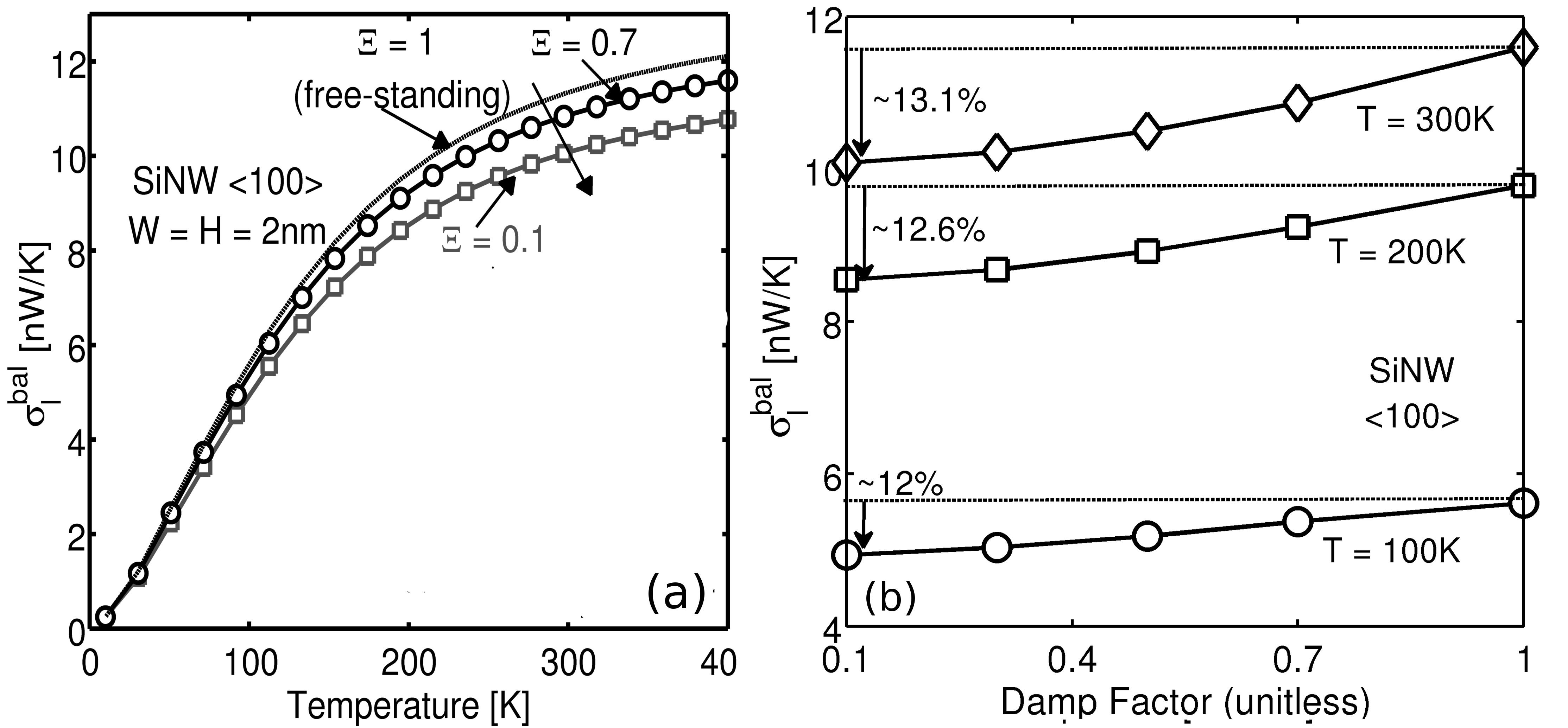
The ballistic for square SiNWs is calculated using their phonon dispersions. The conductance is calculated using Eq. (18) assuming semi-infinite extensions along the wire growth axis (X-axis) and CBC on the periphery (Y and Z axis) of the wire (Fig.3) . Clamping the bottom surface affects the stronger at higher temperature compared to the lower temperature (Fig. 12a). Figure 12b shows the at 300K. The reduction in from free-standing wire to a clamped wire ( = 0.1) is 13.1%. Hence, fixing the surface atoms have a strong impact of the lattice thermal conductance in SiNW.
5 Conclusions
The details for calculating the phonon dispersion in zinc-blende semiconductor structures using the modified Valence Force Field (MVFF) method have been outlined. The MVFF method has been applied to calculate the phonon spectra in confined nanowire structures with varying boundary conditions. The methodology and the computational requirements for the method has been provided. Comparison of original Keating VFF with MVFF shows that, MVFF provides accurate phonon dispersion but at the expense of higher computational demands. Different VFF models can be used for obtaining the solution for physical quantities depending on the type of application, size of the structure and the computational resources available. We believe that the MVFF model will provide better phonon dispersion in ultra-scaled nanostructures. The MVFF method will be crucial in understanding and modeling the thermal properties of ultra-scaled semiconductor devices.
Acknowledgments
The authors would like to acknowledge the computational resources from nanoHUB.org, an National Science Foundation (NSF) funded, NCN project. Financial support from MSD Focus Center, one of six research centers funded under the Focus Center Research Program (FCRP), a Semiconductor Research Corporation (SRC) entity and by the Nanoelectronics Research Initiative (NRI) through the Midwest Institute for Nanoelectronics Discovery (MIND) are also acknowledged.
APPENDICES
Appendix A Details of bulk zinc-blende coplanar interaction
The coplanar interactions are important to obtain the flat nature of the acoustic phonon branches in Si and Ge VFF_mod_herman . There are 21 such interactions in a zinc-blende crystal. The normalized locations of all the atoms involved in the coplanar interactions are shown in Table 9. The corresponding groups used for bulk phonon dispersion calculations are given in Table 10.
| No. | No. | ||||||
|---|---|---|---|---|---|---|---|
| 1* | 0 | 0 | 0 | 14 | 0 | 0.50 | -0.50 |
| 2* | 0.25 | 0.25 | 0.25 | 15 | -0.50 | -0.50 | 0 |
| 3 | 0.25 | -0.25 | -0.25 | 16 | -0.50 | 0 | 0.50 |
| 4 | -0.25 | 0.25 | -0.25 | 17 | 0 | -0.50 | 0.50 |
| 5 | -0.25 | -0.25 | 0.25 | 18 | 0.25 | 0.75 | 0.75 |
| 6 | 0 | 0.50 | 0.50 | 19 | -0.25 | 0.75 | 0.25 |
| 7 | 0.50 | 0 | 0.50 | 20 | -0.25 | 0.25 | 0.75 |
| 8 | 0.50 | 0.50 | 0 | 21 | 0.75 | 0.25 | 0.75 |
| 9 | 0 | -0.50 | -0.50 | 22 | 0.75 | -0.25 | 0.25 |
| 10 | 0.50 | -0.50 | 0 | 23 | 0.25 | -0.25 | 0.75 |
| 11 | 0.50 | 0 | -0.50 | 24 | 0.75 | 0.75 | 0.25 |
| 12 | -0.50 | 0 | -0.50 | 25 | 0.75 | 0.25 | -0.25 |
| 13 | -0.50 | 0.50 | 0 | 26 | 0.25 | 0.75 | -0.25 |
| *Belong to the main bulk unitcell used for DM calculation. | |||||||
| No. | Members | No. | Members | ||||||
|---|---|---|---|---|---|---|---|---|---|
| 1 | 2 | 1 | 3 | 9 | 12 | 1 | 2 | 6 | 18 |
| 2 | 2 | 1 | 4 | 12 | 13 | 1 | 2 | 7 | 21 |
| 3 | 2 | 1 | 5 | 15 | 14 | 1 | 2 | 8 | 24 |
| 4 | 3 | 1 | 2 | 6 | 15 | 6 | 2 | 7 | 22 |
| 5 | 3 | 1 | 4 | 13 | 16 | 6 | 2 | 8 | 25 |
| 6 | 3 | 1 | 5 | 16 | 17 | 7 | 2 | 6 | 19 |
| 7 | 4 | 1 | 2 | 7 | 18 | 7 | 2 | 8 | 26 |
| 8 | 4 | 1 | 3 | 10 | 19 | 8 | 2 | 6 | 20 |
| 9 | 4 | 1 | 5 | 17 | 20 | 8 | 2 | 7 | 23 |
| 10 | 5 | 1 | 2 | 8 | 21 | 5 | 1 | 4 | 14 |
| 11 | 5 | 1 | 3 | 11 | |||||
| *Atom numbers are same as shown in Table 9. | |||||||||
Appendix B Derivation of dynamical matrix from the equation of motion
A crystal in equilibrium has zero total force. However, in the presence of perturbations like lattice vibrations, etc. a small restoring force works on the system. The total force () under small perturbation is given by the Taylor series expansion as,
| (B.1) | |||||
where, N represents all the atoms present in the system and U is the potential energy of the system. In Eq. (B.1) first term in RHS is zero under equilibrium. The next non-zero term is the second term in Eq. (B.1). Under harmonic approximation, only the second term is considered and the higher order (anharmonic) terms are neglected. Now combining Eq. (1) and Eq. (B.1) one can obtain the following,
| (B.2) | |||||
| (B.3) |
where, D is called the ‘Dynamical matrix’ and R is a column vector of displacement for each atom given as,
| (B.4) |
| (B.5) |
Definition of is given in Eq. (2.2).
Appendix C Treatment of surface atoms
The damped displacement of the surface atom ‘j’ can be represented the matrix given as,
| (C.1) |
Taking into account the individual components the displacement vector for the atom ‘j’ we obtain,
| (C.2) |
This modifies eqn.2.2 as,
| (C.3) |
Combining Eq. (C.1) and (C.3) the dynamical matrix component between atom ‘i’ and ‘j’ can be represented as,
| (C.4) |
which can be written in a compressed form as,
| (C.5) |
The value of , where completely free surface atoms have value 1 and completely tied atoms have value 0.
Appendix D Inclusion of mass in the Dynamical matrix
In Eq. (13) the mass of the atoms in on the RHS. It is convenient to include the mass in DM itself. This modifies the the LHS of the equation. The modified DM component between atom ‘i’ and ‘j’ thus, becomes,
| (D.1) |
here and are the masses of atom ‘i’ and ‘j’ respectively. Eq.D.1 can be written in a compressed manner as,
| (D.2) |
where is given as,
| (D.3) |
Appendix E Fitted analytical expressions for DM properties
-
•
Atoms in a 100 SiNW unitcell: The data obtained for the square wires till 6nm 6nm can be fitted to a quadratic polynomial given as,
(E.1) Using Eq. (E.1) for a 16nm 16nm SiNW gives around 7128 atoms.
-
•
Non-zero elements in a 100 SiNW DM: The data for non-zero elements in the DM for SiNW with W till 6nm can be fitted to a quadratic polynomial given by,
(E.2) Using Eq. (E.2) for a 16nm 16nm SiNW yields around 800117 non-zero elements in the DM.
-
•
Relation of NZ elements to in a 100 SiNW: The number of non-zero (NZ) elements vary linearly with the number of atoms (Fig. 13). Fitting the NZ elements with for each wire under study following relations are obtained,
(E.3) (E.4) This shows that the number of NZ elements in MVFF method is roughly twice the NZ elements in KVFF model.
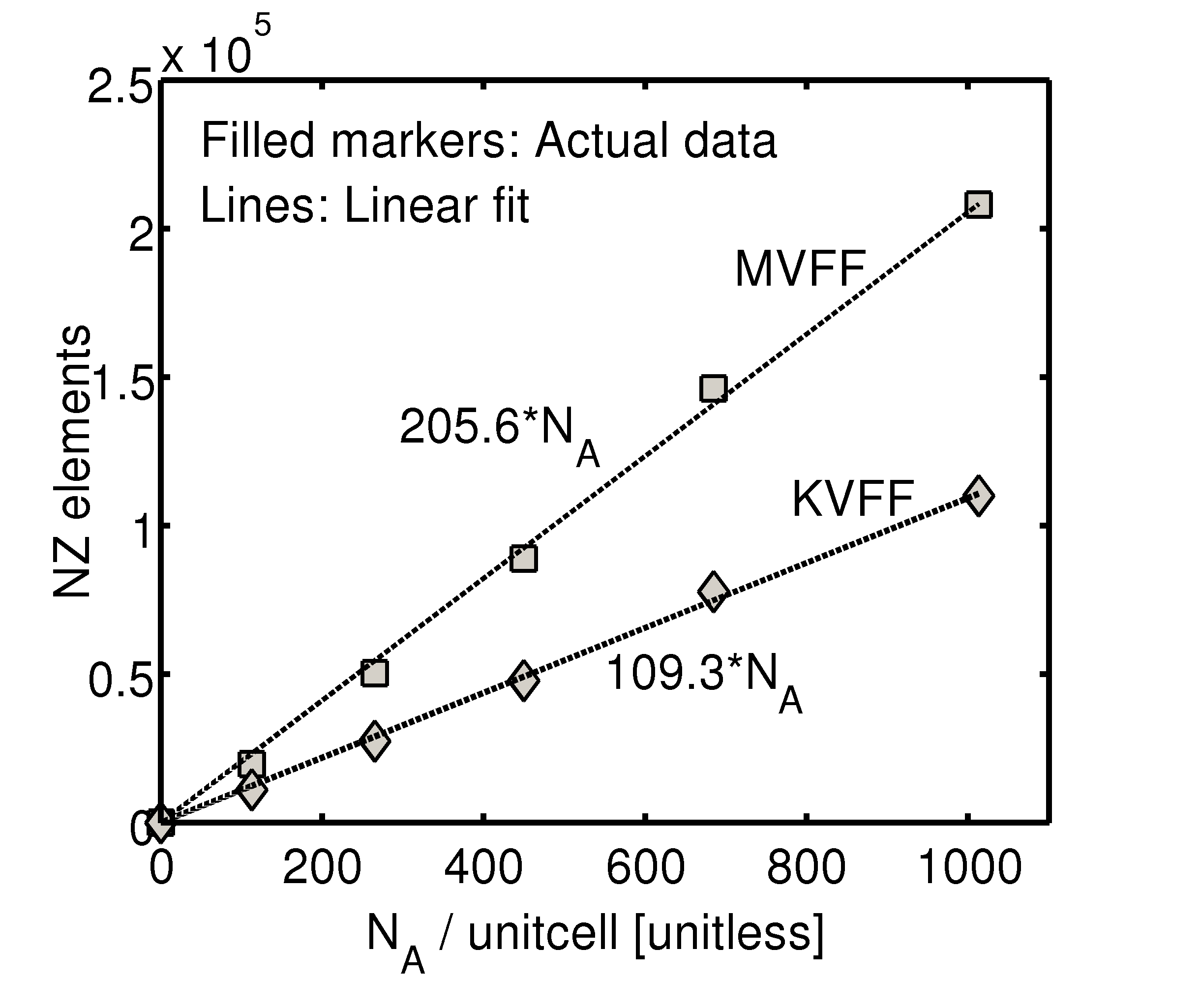
Figure 13: Variation in the number of non-zero (NZ) elements with for the two phonon models (1) Keating VFF and (2) Modified VFF. For both the cases NZ varies linearly with . MVFF has roughly twice the number of NZ elements compared to KVFF model. - •
-
•
Mean assembly time for 100 SiNW DM: The data for mean of the DM for SiNW with W till 6nm can be fitted to a quadratic polynomial given by,
(E.6) Using Eq. (E.6) a 16nm 16nm SiNW DM is estimated to be assembled on single CPU in 226.35 secs.
-
•
Eigen solution time per ‘k’ point for 100 SiNW DM: The eigen values are obtained using the ‘eig’ solver in MATLAB eig_matlab . The time needed for the solution of all the eigen values (with the eigen vectors) for each momentum vector ‘k’ can be fitted to the following expression,
(E.7) Thus, the solution time goes with the sixth power of W. Also this expression gives an estimate time for the solution of one k point using the MATLAB eig solver (on a PC) as 1.19e5 seconds ( 1.4 days). Thus, for very large systems parallel eigen solvers (like SCALAPACK slug ) as well as finding few eigen solutions (using eigs or other sparse eigen solvers, like LAPACK, etc.) is a feasible method.
References
- (1) A. Buin, A. Verma, and M. Anantram, “Carrier-phonon interaction in small cross-sectional silicon nanowires,” Journal of Applid Physics, vol. 104, no. 053716, 2008.
- (2) A. K. Buin, A. Verma, A. Svizhenko, and M. P. Anantram, “Significant Enhancement of Hole Mobility in [110] Silicon Nanowires Compared to Electrons and Bulk Silicon,” Nano Letters, vol. 8, no. 2, pp. 760–765, 2008, pMID: 18205425. [Online]. Available: http://pubs.acs.org/doi/abs/10.1021/nl0727314
- (3) N. Mingo and L. Yang, “Phonon transport in nanowires coated with an amorphous material: An atomistic Green’s function approach,” Phys. Rev. B, vol. 68, no. 24, p. 245406, Dec 2003.
- (4) N. Mingo, L. Yang, D. Li, and A. Majumdar, “Predicting the Thermal Conductivity of Si and Ge Nanowires,” Nano Letters, vol. 3, no. 12, pp. 1713–1716, 2003.
- (5) J. Wang and J.-S. Wang, “Dimensional crossover of thermal conductance in nanowires,” Applied Physics Letters, vol. 90, no. 24, p. 241908, 2007.
- (6) H. Peelaers, B. Partoens, and F. M. Peeters, “Phonon Band Structure of Si Nanowires: A Stability Analysis,” Nano Letters, vol. 9, no. 1, pp. 107–111, 2009.
- (7) P. N. Keating, “Effect of Invariance Requirements on the Elastic Strain Energy of Crystals with Application to the Diamond Structure,” Phys. Rev., vol. 145, no. 2, pp. 637–645, 1966.
- (8) Z. Sui and I. P. Herman, “Effect of strain on phonons in Si, Ge, and Si/Ge heterostructures,” Phys. Rev. B, vol. 48, no. 24, pp. 17 938–17 953, 1993.
- (9) H. Fu, V. Ozolins, and Z. Alex, “Phonons in GaP quantum dots,” Phys. Rev. B, vol. 59, no. 4, pp. 2881–2887, 1999.
- (10) H. McMurry, A. Solbrig Jr., and J. Boyter, “The use of valence force potentials in calculating crystal vibrations,” Journal of Physics and Chemistry of Solids, vol. 28, no. 12, pp. 2359 – 2368, 1967.
- (11) W. Weber, “Adiabatic bond charge model for the phonons in diamond, Si, Ge, and -Sn,” Phys. Rev. B, vol. 15, no. 10, pp. 4789–4803, May 1977.
- (12) K. Rustagi and W. Weber, “Adiabatic Bond charge model for the phonons in A(III)B(V) semiconductors,” Solid State Communications, vol. 18, pp. 673–675, 1976.
- (13) T. Markussen, A.-P. Jauho, and M. Brandbyge, “Heat Conductance Is Strongly Anisotropic for Pristine Silicon Nanowires,” Nano Letters, vol. 8, no. 11, pp. 3771–3775, 2008.
- (14) H. L. McMurry, A. W. Solbrig, B. J. K., and C. Noble, “The use of valence force potentials in calculating crystal vibrations,” J. Phys. Chem. Solids, vol. 28, pp. 2359–2368, 1967.
- (15) J. Zou and A. Balandin, “Phonon heat conduction in a semiconductor nanowire,” Journal of Applied Physics, vol. 89, no. 5, pp. 2932–2938, 2001.
- (16) Y. Zhang, J. X. Cao, Y. Xiao, and X. H. Yan, “Phonon spectrum and specific heat of silicon nanowires,” Journal of Applied Physics, vol. 102, no. 10, p. 104303, 2007.
- (17) X. Li, K. Maute, M. L. Dunn, and R. Yang, “Strain effects on the thermal conductivity of nanostructures,” Phys. Rev. B, vol. 81, no. 24, p. 245318, Jun 2010.
- (18) T. Thonhauser and G. D. Mahan, “Phonon modes in Si [111] nanowires,” Phys. Rev. B, vol. 69, no. 7, p. 075213, Feb 2004.
- (19) H. Zhao, Z. Tang, G. Li, and N. R. Aluru, “Quasiharmonic models for the calculation of thermodynamic properties of crystalline silicon under strain,” Journal of Applied Physics, vol. 99, no. 6, p. 064314, 2006.
- (20) O. L. Lazarenkova, P. von Allmen, F. Oyafuso, S. Lee, and G. Klimeck, “Effect of anharmonicity of the strain energy on band offsets in semiconductor nanostructures,” Applied Physics Letters, vol. 85, no. 18, pp. 4193–4195, 2004.
- (21) Z. W. Hendrikse, M. O. Elout, and W. J. A. Maaskant, “Computation of the independent elements of the dynamical matrix,” Computer Physics Communications, vol. 86, no. 3, pp. 297 – 311, 1995.
- (22) R. Landauer, “Spatial variation of currents and fields due to localized scatterers in metallic conduction,” IBM J. Res. Dev., vol. 1, no. 3, pp. 223–231, 1957.
- (23) D. C. Wallace, “Thermodynamics of Crystals,” Dover Publications, Mineola New York, 1998.
- (24) B. A. Weinstein and G. J. Piermarini, “Raman scattering and phonon dispersion in Si and GaP at very high pressure,” Phys. Rev. B, vol. 12, no. 4, pp. 1172–1186, Aug 1975.
- (25) J. Dongarra, “Survey of Sparse Matrix Storage Formats,” 1995. [Online]. Available: http://www.netlib.org/linalg/html_templates/node90.html
- (26) Mathworks, “Matlab eig reference,” 2010. [Online]. Available: http://www.mathworks.com/help/techdoc/ref/eig.html
- (27) ——, “Matlab eig reference,” 2010. [Online]. Available: http://www.mathworks.com/help/techdoc/ref/eigs.html
- (28) G. Klimeck, F. Oyafuso, T. B. Boykin, R. C. Bowen, and P. von Allmen, “Development of a Nanoelectronic 3-D (NEMO 3-D) Simulator for Multimillion Atom Simulations and Its Application to Alloyed Quantum Dots,” Computer Modeling in Engineering and Science (CMES), vol. 3, no. 5, pp. 601–642, 2002.
- (29) A. Paul, M. Luisier, N. Neophytou, R. Kim, J. Geng, M. McLennan, M. Lundstrom, and G. Klimeck, “Band Structure Lab,” May 2006. [Online]. Available: http://nanohub.org/resources/1308
- (30) G. Nilsson and G. Nelin, “Study of the Homology between Silicon and Germanium by Thermal Neutron Spectrometry,” Phys. Rev. B, vol. 6, no. 10, pp. 3777–3786, 1972.
- (31) “Electronic archive, New Semiconductor Materials - Characteristics and Properties,” Ioffe Physico-Technical Institute Website, 2001, http://www.ioffe.ru/SVA/NSM/Semicond/.
- (32) O. Madelung, “Semiconductors - HandBook,” Springer 3rd ed., 2004.
- (33) S. de Gironcoli, “Phonons in Si-Ge systems: An ab initio interatomic-force-constant approach,” Phys. Rev. B, vol. 46, no. 4, pp. 2412–2419, Jul 1992.
- (34) R. Eryiğit and I. P. Herman, “Lattice properties of strained GaAs, Si, and Ge using a modified bond-charge model,” Phys. Rev. B, vol. 53, no. 12, pp. 7775–7784, Mar 1996.
- (35) O. L. Lazarenkova, P. von Allmen, F. Oyafuso, S. Lee, and G. Klimeck, “An atomistic model for the simulation of acoustic phonons, strain distribution, and Grüneisen coefficients in zinc-blende semiconductors,” Superlattices and Microstructures, vol. 34, no. 3-6, pp. 553 – 556, 2003.
- (36) L. S. Blackford, J. Choi, A. Cleary, E. D’Azevedo, J. Demmel, I. Dhillon, J. Dongarra, S. Hammarling, G. Henry, A. Petitet, K. Stanley, D. Walker, and R. C. Whaley, ScaLAPACK Users’ Guide. Philadelphia, PA: Society for Industrial and Applied Mathematics, 1997.