Neuromorphic, Digital and Quantum Computation with Memory Circuit Elements
Abstract
Memory effects are ubiquitous in nature and the class of memory circuit elements - which includes memristive, memcapacitive and meminductive systems - shows great potential to understand and simulate the associated physical processes. Here, we show that such elements can also be used in electronic schemes mimicking biologically-inspired computer architectures, performing digital logic and arithmetic operations, and can expand the capabilities of certain quantum computation schemes. In particular, we will discuss some examples where the concept of memory elements is relevant to the realization of associative memory in neuronal circuits, spike-timing-dependent plasticity of synapses, digital and field-programmable quantum computing.
Index Terms:
Memory, Resistance, Capacitance, Inductance, Dynamic response, Hysteresis.I Introduction
Memristive [1, 2], memcapacitive and meminductive [3] systems constitute an important class of two-terminal circuit elements whose basic characteristics - namely, their resistance, capacitance and inductance - retain memory of the past states through which the systems have evolved. The memory features of these systems are related to corresponding internal states of these elements (e.g., atomic structure [4], spin polarization [5, 6], etc.) which can be influenced by an external control parameter like the voltage, charge, current or flux.
Mathematically, th-order -controlled memory elements are defined by the relations [3]
| (1) | |||||
| (2) |
where denotes a set of state variables describing the internal state of the system, and are any two fundamental circuit variables (i.e., current, charge, voltage, or flux) denoting input and output of the system, is a generalized response, and is a continuous -dimensional vector function. The different memory elements are determined by three pairs of circuit variables: current-voltage (memristive systems), charge-voltage (memcapacitive systems), and flux-current (meminductive systems). Two other pairs (charge-current and voltage-flux) are linked through equations of electrodynamics, and therefore do not give rise to any new element. Devices defined by the relation of charge and flux (which is the time integral of the voltage) are not considered as a separate group since such devices can be redefined in the current-voltage basis [1]. Moreover, we note that memristors, memcapacitors and meminductors are ideal (and rare) instances of memristive, memcapacitive and meminductive systems, respectively (see Refs. [1, 3, 7]). In this work, the terms memristors, memcapacitors and meminductors are reserved only for such ideal cases.
These memory systems turn out to be of very general interest in science and engineering and are potentially useful not just in information storage but also in apparently different areas of research [8, 9, 10, 11, 12, 13, 14, 15, 16, 17, 18, 19, 20, 7]. Of equal importance and arguably the less studied of all these applications so far, memory elements may be of use in the three different paradigms of computation: analog, digital, and quantum. This is the subject of this paper.
In the case of analog computation, it was recently shown that electronic circuits with memory circuit elements [3] can simulate processes typical of biological systems such as the adaptive behavior of unicellular organisms [10], learning and associative memory [16]. The concept of “learning circuits” has also been implemented recently using VO2 as memory element [20]. Here, we first briefly discuss existing memristive models of neural computing as well as realization of spike-timing-dependent plasticity (STDP) with first-order memristive systems. Then, we formulate a model of a second-order memristive synapse which resembles closer the operation of its biological counterpart.
The implementation of classical logic operations with memristive systems was discussed theoretically in the past (see e.g. Refs. [21, 22, 11]) and demonstrated experimentally [18]. In this paper, we suggest a different scheme for classical logic operations utilizing a combination of memcapacitive and memristive systems. Our scheme realizes all basic logic operations (NOT, OR, AND) as well as many other operations (XOR, multi-input OR, AND, etc.) in a much simpler way as compared to the alternative approaches [11, 18]. In addition, it provides a significant speed-up of operations. In this paper, we demonstrate experimentally for the first time addition of two one-bit numbers using memory circuit elements. Our scheme requires only 16 steps compared to 87 steps as suggested in a previous approach [11]. Also, it is worth stressing that in these cases computing and memory are integrated in the same platform, which is a major conceptual departure from present-day computing technology where memory and computing are physically disjoint.
Finally, in the case of quantum computation we discuss specific quantum computing schemes where meminductive and memcapacitive systems could be used to generate an essentially infinite number of programmable interaction Hamiltonians between two or more qubits inductively or capacitively coupled, in a manner we could term field-programmable quantum computation, the quantum analog of the well-established classical field-programmable gate array. This opens up the possibility of expanding both our fundamental understanding of circuit quantum electrodynamics [23, 24] as well as the optimization of quantum computing algorithms.
II Neural computation with memristive systems
Neuromorphic computing circuits are designed by borrowing principles of operation typical of the human (or animal) brain and, therefore, due to their intrinsic analog capabilities they can potentially solve problems that are cumbersome (or outright intractable) by digital computation. Examples of such problems include - but are not limited to - adaptive behavior, learning by association, pattern recognition, fuzzy logic, etc. Certain realizations of memristive systems can be very useful in such circuits because of their intrinsic properties which mimic to some extent the behavior of biological synapses. In addition, the most recent experimental realizations of memory elements pertain to systems of dimensions in the nanometer regime [25, 26], thus allowing a possible scale-up of such elements in a chip to the number density of a typical human brain (consisting of about 1011 synapses/cm3). In the following we first briefly review our work on memristive neural networks (MNNs) showing a practical realization of the Hebbian learning, which states, in a very simplified form, that “neurons that fire together, wire together”.
We then discuss one of the most important functions of synapses namely their spike-timing-dependent plasticity [27, 28, 29, 30]. The existing experimental approaches to STDP are based on relatively large-size VLSI circuits [31, 32, 33, 34], three terminal transistor-like structures based on ionic conduction [15] or combination of memristive systems with CMOS elements [19]. Below, we discuss two different memristive system-based schemes in which STDP can be realized. In the first, we may call “bipolar”, first-order memristive systems probed by two composite pulses overlapping in time develop STDP. This is similar to what has been studied in [35, 36, 37, 38]. In the second realization, we could call “intrinsic”, we provide a model of a memristive system which at the prize of increasing the number of state variables to two, does show STDP even if the excitation pulses do not overlap temporally. This situation is closer to the actual operation of a biological synapse in which each synaptic event triggers a cascade of internal decaying processes/reactions.
II-A Memristive neural networks and Hebbian learning
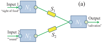
In Fig. 1(a) we show a simple MNN consisting of two memristive systems mimicking the behavior of synapses and three electronic neurons (two input and one output) whose role is to monitor their inputs and send (in both forward and backward directions) signals of a given intensity and shape [16]. This network belongs to a wide class of asynchronous (stochastic) neural networks [39], namely, networks with probabilistic neuron firing. In Ref. [16] we have implemented the behavior of the electronic neurons using an analog-to-digital converter and a microcontroller, so that once the input voltage exceeds a threshold voltage, both forward (of positive polarity) and backward (of negative polarity) pulses are generated whose amplitude is constant, but pulse separation varies according to the amplitude of the input signal. The basic synaptic activity of two electronic synapses ( and in Fig. 1(a)) has been achieved using memristor emulators [10, 16, 17] pre-programmed with equations of a threshold-type first-order memristive system [10]:
| (3) | |||||
| (4) | |||||
where and are the current through and the voltage drop on the device, respectively, and is the internal state variable playing the role of memristance, , is the step function, and characterize the rate of memristance change at and , respectively, is a threshold voltage, and and are limiting values of the memristance . In Eq. (4), the -functions symbolically show that the memristance can change only between and . 111In the actual microcontroller’s software implementation, the value of is monitored at each time step and in the situations when or , it is set equal to or , respectively. In this way, we avoid situations when may overshoot the limiting values by some amount and thus not change any longer because of the step function in Eq. (4).
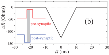
When and is above the amplitude of the forward (pre-synaptic) pulse but does not exceed its doubled amplitude, the change in memristance () is possible only when forward (from or ) and backward (from ) pulses overlap. This can be clearly seen if we rewrite Eq. (4) at (omitting -functions) as
| (5) |
Fig. 1(b) shows the dependence of on the relative pulse timing. The maximum change of memristance occurs when the pulse overlap is perfect ().
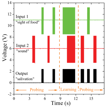
This memristive synapse allows the implementation of the simplest learning rule: Hebbian learning. In fact, if we allow both input electronic neurons to fire at random times, potentiation of the conditioned memristive system would occur only when the signal of the output neuron overlaps in time with the signal coming from neuron . In this case, the second synaptic connection is driven from a high-resistance to a low-resistance state since the voltage drop across exceeds the threshold value due to the simultaneous excitation of both input neurons (the first one exciting in turn the output neuron). This is shown in Fig. 2 where a detail of this process is described.
II-B Spike-timing-dependent plasticity
However, biological synapses show a much more complicated plasticity (with time-resolved properties) [27, 28, 29, 30] than the above simple Hebbian rule seems to suggest. In fact, when a post-synaptic signal reaches the synapse before the action potential of the pre-synaptic neuron, the synapse shows long-term depression (LTD), namely its strength decreases (smaller connection between the neurons) depending on the time difference between the post-synaptic and the pre-synaptic signals. Conversely, when the post-synaptic action potential reaches the synapse after the pre-synaptic action potential, the synapse undergoes a long-time potentiation (LTP), namely the signal transmission between the two neurons increases in proportion to the time difference between the pre-synaptic and the post-synaptic signals. These general features can be implemented using different types of memristive systems.
II-B1 STDP with first-order memristive systems
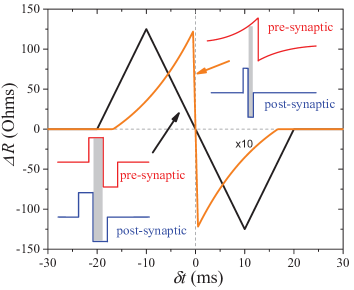
The spike-timing-dependent plasticity with first-order memristive systems can be achieved by application of bipolar pulses corresponding to pre-synaptic and post-synaptic action potential pulses. In order to achieve STDP on time scales similar to those encountered in biological synapses, the pulse width should be of the order of 20ms since the memristance modification with this type of memristive systems is possible only during pulses overlap. Fig. 3 demonstrates modification of memristance induced by a pair of rectangular double pulses and also shows the effect of a non-linear and rectangular double pulse on the memristance . In both cases we observe memristance changes only in a finite time window. Although rectangular double pulses are easier to generate, the use of a non-linear pulse demonstrates a closer similarity of memristance change to the variation of synaptic strength in biological systems.
We also note that the approach to synaptic plasticity using wide pulses may require reconsideration of rules governing the neural network operation. For example, it is not quite clear how to model multiple pre-synaptic pulses that are fired with a time interval shorter than their pulse length. In this publication, we are not going to focus on such issues and discuss only possible realizations of STDP with memristive synapses.
II-B2 STDP with second-order memristive systems
Having discussed spike-timing-dependent plasticity with first-order memristive systems, let us consider STDP with higher-order memristive systems. The advantage of using higher-order memristive systems is related to their multiple state variables that can make the operation of an artificial synapse closer to the operation of its biological counterpart. In particular, we will focus on second-order memristive systems whose internal state, by definition [2, 3], is described by two state variables. In our model given below, the second state variable is used to track the time separation between pre-synaptic and post-synaptic action potential pulses.
We consider a second-order memristive system described by the following equations
| (6) | |||||
| (7) | |||||
| (8) | |||||
where and are internal state variables, is a constant, , is a threshold voltage, is a threshold value of , is a constant defining the time window of STDP. It is assumed that short (e.g., ms width) pre-synaptic and post-synaptic square pulses of the same polarity are applied to the second-order memristive system. According to Eq. (7), the memristance can change when . The change of is described by Eq. (8) whose right-hand side contains excitation terms involving -functions and a relaxation term . Therefore, after being excited, the decay of the variable occurs with a decay constant . The particular combination of -functions in this equation defines the excitation rules: i) the excitation is possible only when and ii) the variable excited by a certain polarity of the voltage applied to the memristive system ( is given by a difference of pre-synaptic and post-synaptic potentials) can not be re-excited by a pulse of opposite polarity if . We also note that the change in memristance described by Eqs. (6-8) is unconstrained as we are interested only in small changes in . The constraints on the minimal and maximum values of can be introduced as it is done in Eqs. (3-4).
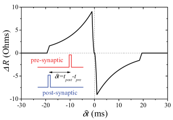
A numerically calculated change in memristance as a function of the time interval between the pulses is shown in Fig. 4. This plot is very similar to synaptic weight changes observed in experiments with biological synapses [27, 28, 29, 30] thus lending support to this type of model.
The use of second-order memristive systems in memristive neural networks is very promising since neuron’s firing can be implemented simply by short single rectangular pulses with no additional hardware, which is instead needed, for example, to obtain this type of functionality with only first-order memristive systems (as in Ref. [19]). However, such solid-state second-order memristive systems need to be developed, even though their implementation in memristor emulators [10, 16, 17] is straightforward. Moreover, we would like to mention that Eqs. (6-8) provide one of the simplest possible models of second-order memristive systems exhibiting STDP. For instance, abrupt -functions entering these equations can be replaced by sigmoidal functions thus providing a smoother analytical behavior.
III Logic gates and arithmetics with memory circuit elements
In this section, we discuss logic and arithmetic operations performed by the circuit shown in Fig. 5 which comprises an array of memristive systems, a memcapacitive system, a load resistor and drivers. In this type of application, each memristive system is used in the “digital” mode of operation, namely only one bit of information is encoded in the memristor’s state. We call “1” (ON) the state of lower resistance and “0” (OFF) that of higher resistance. The operation of the circuit sketched in Fig. 5 relies on charging a memcapacitive system through input memristive system and subsequent discharging through the output ones. In this way, the basic logic operations (NOT, OR, AND) as well as many other operations (XOR, multi-input OR, AND, etc.) are realized in a much simpler fashion than in existing approaches based on memristive systems only [11, 18]. More complex operations (e.g., addition) can be performed by sequences of the elementary logic operations mentioned above.
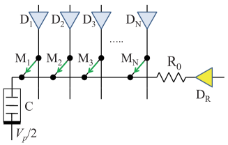
Using four memristor emulators [17, 16, 40], we have built the circuit described in Fig. 5 and used it to demonstrate the full set of basic Boolean logic operations as well as addition of two one-bit numbers. The extension of such a circuit to operations with multi-bit numbers is straightforward and is not reported here. In fact, the addition of two -bit numbers in this architecture requires memristive systems ( memristive systems are used to store initial values, memristive systems are reserved for the calculation result and 1 memristive system is used as a carry flag). In the circuit shown in Fig. 5 the initial values are not destroyed and can be reused later. The circuit uses three-state drivers (with voltage states: 0V, , not-connected) connected to memristive systems, and four-state driver (0V, , , not-connected) connected to the resistor R0.
Although memcapacitor (as well as meminductor) emulators can also be built using simple electronic schemes [40, 41], their models are not yet well developed. Moreover, the noise reduction is a very important task in experiments with such schemes [40]. Therefore, in our circuit realization we have employed a usual F capacitor in place of the memcapacitive system. We will later discuss the advantages of replacing the regular capacitor with a memcapacitor.
In order to understand the circuit operation, we first note that the circuit employs threshold-type bipolar memristive systems such as the TiO2 memristive systems recently demonstrated experimentally [4]. To represent this situation we have implemented the equations (3) and (4) in our memristor emulator [10, 16, 17]. In this case, the change of memristance occurs only if the applied voltage exceeds the threshold voltage of the device. In addition, for successful circuit operation, the value of should be selected between and . In this case, the charging of from the completely discharged state will never alter the value of input memristive systems (since during this process voltages applied to input memristive systems do not exceed ).
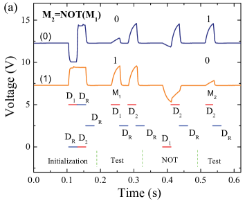
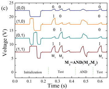
The circuit operation consists of a sequence of the following elementary operations: 1) capacitor initialization (by application of voltage pulse by D driver), 2) initialization of memristive systems’ states (by application of 0 or voltage pulse by D driver simultaneously with or 0 voltage pulse by one of D1-D4 drivers), 3) capacitor charging through an input memristive system (by application of 0 or voltage pulse by one of the D1-D4 drivers), and 4) capacitor discharge through an output memristive system (by application of or 0 voltage pulse by one of D1-D4 drivers). Note, that in the operations used by us the current can flow only through one memristive system at any one time. Namely, after the capacitor has been charged through the input memristive system, the latter is disconnected (its driver is switched into ”not connected” state) and the output memristive system is connected to allow capacitance discharge. 222Note that the switching of driver states can be done very fast. The parameter values specific to our circuit realization are: V, V, and 25ms is the width of initialization and reset pulses. An example of sequences of voltage drivers necessary to create the NOT gate is shown in Fig. 6(a). Having discussed elementary circuit operations, let us now turn to implementation of basic Boolean operations.
NOT gate - M2 = NOT(M1) - 4 steps - This operation is realized according to the following sequence of operations (see also Fig. 6(a)): set M, reset C, charge C through M1 by 0V pulse of a finite width applied by D1, discharge C through M2 by pulse applied to D2. The main idea is that the capacitor C can only be charged to a sufficiently high voltage to switch M2 to zero if M. Therefore, if M then M and if M then M. This is the logical NOT operation.
Going into measurement details, in the initialization phase (Fig. 6(a)) we set M and M (top curve (0)) or M (curve (1)) by application of 25ms pulses by D1, D2 and D drivers as described above. In the first testing phase, we monitor the memristance of M1 and M2 by consecutive application of positive 25ms pulses by D1 and D2 drivers to corresponding memristive systems as well as capacitor reset pulses. In this way, is charged through the memristive systems and the charging rate provides information about memristive systems’ states. Then, we reset C, charge C through M1 by 25ms 0V pulse, discharge C through M2 by 25ms pulse. In the final testing phase, the value of is monitored via the rate of the capacitor charging, again via application of a 25ms pulse to M2. If the voltage across the capacitor does not change much then the state of M2 is : high-resistance state and thus low current flows to the capacitor plates. Conversely, if the voltage across the capacitor does change faster to then the state of M2 is : low-resistance state and thus more charges accumulate on the capacitor plates. For the purpose of clarity, the sequence of applied pulses is shown in the bottom of Fig. 6(a) in absolute scale for the realization of the top sequence of Fig. 6(a). All other curves are shifted for clarity.
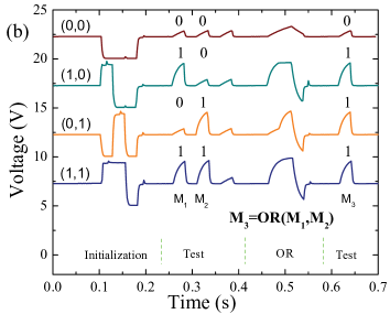
OR gate - M3 = OR(M1,M2) - 5 steps - This is implemented by the following sequence: M, reset C, charge C through M1 by pulse, charge C through M2 by pulse, discharge C through M3 by 0V pulse. The width of all pulses in this sequence is 25ms. Figure 6(b) shows four voltage lines corresponding to different initial states of M1 and M2 memristive systems. The correct truth table of the OR gate is clearly identified during the second testing phase in Fig. 6(b).
AND gate - M3 = AND(M1,M2) - 5 steps - The sequence for this logic gate is as follows: M, reset C, charge C through M1 by a short pulse, charge C through M2 by a short pulse, discharge C through M3 by 0V pulse. In the AND operation, the width of short pulses is equal to 10ms and the width of all other pulses is 25ms. The width of short charging pulses is selected in such a way that both M1 and M2 memristive systems should be in the ON state in order to charge to such a voltage so that during the next step, namely during the capacitor discharge through M3, the latter is switched into the ON state. Fig. 6(c) shows results demonstrating correct implementation of the AND gate.
XOR gate - M3 = XOR(M1,M2) - 11 steps - This is realized by the following sequence: M, reset C, charge C through M1 by a short pulse, discharge C through M2 by a short V pulse, charge C through M1 by a short pulse, discharge C through M3 by 0-V pulse, reset C, charge C through M2 by a short pulse, discharge C through M1 by a short V pulse, charge C through M2 by a short pulse, discharge C through M3 by 0-V pulse. Similarly to the AND gate, the duration of short pulses is 10 ms and that of all other pulses is 25 ms.
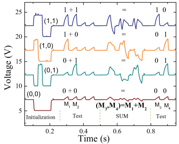
Addition of two 1-bit numbers - 16 steps - Next, we consider the addition of two one-bit numbers that we encode in M1 and M2 memristive systems. The result of addition is saved in M3 and M4 memristive systems. It is easy to check that the addition can be performed with the sequence M3=AND(M1,M2) and M4=XOR(M1,M2). In Fig. 7 we show experimentally measured signal patterns that prove the above operation. We emphasize that an approach suggested previously [11] would require 87 steps to perform the same operation.
At this point, we would like to re-emphasize that the extension of our scheme to the addition of -bit numbers is straightforward. In particular, the -th bit of the result will be given by a sum of the two -th bits of the input numbers and the carry flag, from the summation of the -1 bits. In the case of the one-bit addition considered in the present work, the carry flag is encoded in the M4 memristive system. Moreover, we want to stress that the circuit operation can be further optimized if we use a memcapacitive system as shown in Fig. 5 (instead of the usual capacitor implemented here). In this case, the state of the memcapacitive system can evolve when pulses are applied to those memristive systems that store the initial values. Therefore, some computation results can be temporarily stored in the memcapacitive system state thus decreasing the number of computation steps required.
Finally, we would like to mention that the crossbar architectures - formed by “vertical” and “horizontal” sets of wires - typically used to fabricate nanoscale memristive systems [25, 26, 13] may allow an effective parallelization of the arithmetic and logic operations we have described here. For instance, the application of pulses to “vertical” wires would cause a computation within each horizontal line in parallel. Moreover, switching the role of horizontal and vertical wires would cause a switch of computation direction. In this way, interesting and more complex computational schemes can be practically realized. However, a practical realization of such a scheme may require use of highly nonlinear memristive systems or additional switches/individual access devices in order to avoid unwanted currents that naturally appear in a resistive network. In addition, if unwanted currents can be eliminated or reduced, this massive parallelization may offset intrinsically slower switching times of memristive systems (ns) in comparison with typically shorter switching times of, e.g., CMOS-based elements performing arithmetic operations.
IV Quantum computation with memory elements
It seems timely to consider the potentialities of memory elements - in particular low-dissipative meminductive and memcapacitive systems - in quantum computation, which is based on the unitary evolution of a quantum system. Although many experimental systems have been suggested as quantum bits (qubits) [42, 43, 44, 45, 46], here we will focus on superconducting (SC) qubits [46, 47] that currently are considered among the most promising ones. Since typical SC qubit circuits involve capacitors and inductors, memcapacitive and meminductive systems fit naturally in this application.
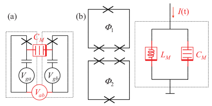
Field-programmable quantum computation - In SC quantum computation schemes, phase and charge qubits are coupled capacitively while flux qubits are coupled inductively [47]. Memcapacitive and meminductive systems can be used in such schemes to provide a controllable interaction between SC qubits 333The range of possible applications of memory elements in quantum computing is not limited to this situation, and we indeed anticipate many other different opportunities. For instance, a micromechanical resonator embedded into a DC SQUID [48] results in an effective meminductive system. In addition, a lagging of SC qubit s due to memory effects in inductance was recently discussed [49].. For example, let us consider two charge qubits [50, 51] interacting via a usual capacitive coupling. The corresponding coupling term has the form [47]
| (9) |
where is the elementary charge and are the -component Pauli matrices acting on the wave function of the corresponding qubit in the reduced Hilbert subspace. We can now replace the capacitor by a memcapacitive system and insert a controllable voltage source between the qubits (see Fig. 8(a)). Alternatively, can be directly connected in parallel with the memcapacitive system. This last scheme, however, may induce large currents in the two qubits if the qubits circuits are grounded thus perturbing them incoherently. Either way, the value of the memcapacitance - that replaces in Eq. (9) - can be pre-set and the interaction Hamiltonian will depend on this pre-set value of capacitance. For two interacting qubits the magnitude of the interaction strength is not very important as it can be compensated by the interaction time. However, if we consider simultaneously interacting qubits then a variation of coupling between two of them will result in absolutely different interaction Hamiltonians thus leading to a different system evolution. Quantum computation algorithms will thus benefit from such novel quantum hardware functionality because of the many (practically infinite) interaction schemes that can be implemented within a single device architecture.
In the case of flux qubits the latter can be controlled, via mutual inductance, by a tank circuit consisting of a meminductive system with a regular capacitor or possibly a memcapacitive system as shown in Fig. 8 (b). The tank circuit may be current- or voltage-controlled and by setting the different values of meminductance, and memcapacitance, , its frequency changes thus leading to a different interaction Hamiltonian between the two qubits. Again, in the case of interacting qubits this leads to a large number of time evolutions and thus different computation schemes. Because of the similarity to classical field-programmable gate arrays, we could term the above two computation architectures as “field-programmable quantum computation”. Some work is however needed to realize such an architecture practically, in particular, to avoid additional decoherence effects that can be introduced by real memcapacitive/meminductive elements [52, 53, 12, 54, 55, 56].
V Conclusions
In conclusion, we have addressed all three different paradigms of computation - neuromorphic (analog), digital and quantum - and shown the potential the three classes of memory elements, namely memristive, memcapacitive and meminductive systems offer in all three cases. In particular, we have discussed memristive neural networks, classical logic and arithmetic operations with memristive and memcapacitive systems, and field-programmable quantum computation with meminductive and memcapacitive systems with both charge and flux qubits. Clearly, much work needs to be done to advance these applications. Important issues include, e.g., realization of high connectivity in neural networks (each neuron in the human brain has 7000 synaptic connections), effective parallelization of logic and arithmetic operations, reduction of qubit decoherence, etc. In spite of these difficulties, with the increasing research into actual materials and devices that behave as memory elements we anticipate many more ideas could be implemented in actual systems and circuits thus offering a wider range of opportunities even in hybrid computational schemes involving any two, or even all three paradigms.
Acknowledgment
M.D. acknowledges partial support from the National Science Foundation (DMR-0802830). We thank Ben Criger and Frank Wilhelm for getting us interested in the possible use of memory elements in quantum computation and for useful discussions.
References
- [1] L. O. Chua, “Memristor - the missing circuit element,” IEEE Trans. Circuit Theory, vol. 18, pp. 507–519, 1971.
- [2] L. O. Chua and S. M. Kang, “Memristive devices and systems,” Proc. IEEE, vol. 64, pp. 209–223, 1976.
- [3] M. Di Ventra, Y. V. Pershin, and L. O. Chua, “Circuit elements with memory: Memristors, memcapacitors, and meminductors,” Proc. IEEE, vol. 97, no. 10, pp. 1717–1724, 2009.
- [4] J. J. Yang, M. D. Pickett, X. Li, D. A. A. Ohlberg, D. R. Stewart, and R. S. Williams, “Memristive switching mechanism for metal/oxide/metal nanodevices,” Nat. Nanotechnol., vol. 3, pp. 429–433, 2008.
- [5] Y. V. Pershin and M. Di Ventra, “Spin memristive systems: Spin memory effects in semiconductor spintronics,” Phys. Rev. B, vol. 78, p. 113309, 2008.
- [6] X. Wang, Y. Chen, H. Xi, H. Li, and D. Dimitrov, “Spintronic memristor through spin-torque-induced magnetization motion,” El. Dev. Lett., vol. 30, pp. 294 – 297, 2009.
- [7] Y. V. Pershin and M. Di Ventra, “Memory effects in complex materials and nanoscale systems,” Advances in Physics, vol. 60, pp. 145–227, 2011.
- [8] P. Kuekes, D. Stewart, and R. Williams, “The crossbar latch: Logic value storage, restoration, and inversion in crossbar circuits,” J. Appl. Phys., vol. 97, p. 034301, 2005.
- [9] T. Driscoll, H.-T. Kim, B. G. Chae, M. Di Ventra, and D. N. Basov, “Phase-transition driven memristive system,” Appl. Phys. Lett., vol. 95, pp. 043 503–1–043 503–3, 2009.
- [10] Y. V. Pershin, S. La Fontaine, and M. Di Ventra, “Memristive model of amoeba learning,” Phys. Rev. E, vol. 80, pp. 021 926–1–021 926–6, 2009.
- [11] E. Lehtonen and M. Laiho, “Stateful implication logic with memristors,” in Proceedings of the 2009 International Symposium on Nanoscale Architectures (NANOARCH’09)), 2009, pp. 33 – 36.
- [12] T. Driscoll, H.-T. Kim, B.-G. Chae, B.-J. Kim, Y.-W. Lee, N. M. Jokerst, S. Palit, D. R. Smith, M. Di Ventra, and D. N. Basov, “Memory metamaterials,” Science, vol. 325, pp. 1518–1521, 2009.
- [13] J. Borghetti, Z. Li, J. Straznicky, X. Li, D. A. A. Ohlberg, W. Wu, D. R. Stewart, and R. S. Williams, “A hybrid nanomemristor/transistor logic circuit capable of self-programming,” Proc. Nat. Ac. Sci., vol. 106, pp. 1699–1703, 2009.
- [14] N. Gergel-Hackett, B. Hamadani, B. Dunlap, J. Suehle, C. Richter, C. Hacker, and D. Gundlach, “A Flexible Solution-Processed Memristor,” IEEE El. Dev. Lett., vol. 30, pp. 706–708, 2009.
- [15] Q. Lai, L. Zhang, Z. Li, W. F. Stickle, R. S. Williams, and Y. Chen, “Ionic/electronic hybrid materials integrated in a synaptic transistor with signal processing and learning functions,” Adv. Mat., vol. 22, p. 2448, 2010.
- [16] Y. V. Pershin and M. Di Ventra, “Experimental demonstration of associative memory with memristive neural networks,” Neural Networks, vol. 23, p. 881, 2010.
- [17] ——, “Practical approach to programmable analog circuits with memristors,” IEEE Trans. Circ. Syst. I, vol. 57, p. 1857, 2010.
- [18] J. Borghetti, G. S. Snider, P. J. Kuekes, J. J. Yang, D. R. Stewart, and R. S. Williams, “‘Memristive’ switches enable ‘stateful’ logic operations via material implication,” Nature, vol. 464, pp. 873–876, 2010.
- [19] S. H. Jo, T. Chang, I. Ebong, B. B. Bhadviya, P. Mazumder, and W. Lu, “Nanoscale memristor device as synapse in neuromorphic systems,” Nano Lett., vol. 10, pp. 1297–1301, 2010.
- [20] T. Driscoll, J. Quinn, S. Klein, H. T. Kim, B. J. Kim, Y. V. Pershin, M. Di Ventra, and D. N. Basov, “Memristive adaptive filters,” Apl. Phys. Lett., vol. 97, p. 093502, 2010.
- [21] D. Strukov and K. Likharev, “CMOL FPGA: a reconfigurable architecture for hybrid digital circuits with two-terminal nanodevices,” Nanotechn., vol. 16, pp. 888–900, 2005.
- [22] G. S. Snider and R. S. Williams, “Nano/CMOS architectures using a field-programmable nanowire interconnect,” Nanotechnology, vol. 18, p. 035204, 2007.
- [23] A. Blais, R.-S. Huang, A. Wallraff, S. M. Girvin, and R. J. Schoelkopf, “Cavity quantum electrodynamics for superconducting electrical circuits: An architecture for quantum computation,” Phys. Rev. A, vol. 69, p. 062320, 2004.
- [24] A. Wallraff, D. Schuster, A. Blais, L. Frunzio, R. Huang, J. Majer, S. Kumar, S. Girvin, and R. Schoelkopf, “Strong coupling of a single photon to a superconducting qubit using circuit quantum electrodynamics,” Nature, vol. 431, pp. 162–167, 2004.
- [25] J. J. Yang, J. Borghetti, D. Murphy, D. R. Stewart, and R. S. Williams, “A Family of Electronically Reconfiguiable Nanodevices,” Adv. Mat., vol. 21, pp. 3754–3758, 2009.
- [26] S. H. Jo, K.-H. Kim, and W. Lu, “High-density crossbar arrays based on a si memristive system,” Nano Lett., vol. 9, pp. 870–874, 2009.
- [27] W. B. Levy and O. Steward, “Temporal contiguity requirements for long-term associative potentiation depression in the hippocampus,” Neuroscience, vol. 8, pp. 791–797, 1983.
- [28] H. Markram, J. Lubke, M. Frotscher, and B. Sakmann, “Regulation of synaptic efficacy by coincidence of postsynaptic APs and EPSPs,” Science, vol. 275, pp. 213–215, 1997.
- [29] G. Q. Bi and M. M. Poo, “Synaptic modifications in cultured hippocampal neurons: dependence on spike timing, synaptic strength and postsynaptic cell type,” J. Neurosci., vol. 18, pp. 10 464–10 472, 1998.
- [30] R. C. Froemke and Y. Dan, “Spike-timing-dependent synaptic modification induced by natural spike trains,” Nature, vol. 416, pp. 433–438, 2002.
- [31] A. Bofill, A. F. Murray, and D. P. Thompson, “Circuits for VLSI implementation of temporally asymmetric Hebbian learning,” in Advances in Neural Information Processing Systems, T. G. Dietterich, S. Becker, and Z. Ghahramani, Eds. MIT Press, 2001, vol. 14, p. 1091.
- [32] B. Glackin, T. McGinnity, L. Maguire, Q. Wu, and A. Belatreche, “A novel approach for the implementation of large scale spiking neural networks on FPGA hardware,” in Proc. IWANN 2005 Computational Intellingence and Bioinspired Systems, Barcelona, Spain, June 2005, pp. 552–563.
- [33] J. Arthur and K. Boahen, “Learning in silicon: Timing is everything,” in Advances in Neural Information Processing Systems, B. Sholkopf and Y. Weiss, Eds. MIT Press, 2006, vol. 18, pp. 75–82.
- [34] G. Indiveri, E. Chicca, and R. Douglas, “A VLSI array of low-power spiking neurons and bistable synapses with spike-timing dependent plasticity,” IEEE Transactions on Neural Networks, vol. 17, pp. 211–221, 2006.
- [35] G. S. Snider, “Cortical computing with memristive nanodevices,” SciDAC Review, vol. 10, pp. 58–65, 2008.
- [36] A. Afifi, A. Ayatollahi, and F. Raissi, “Stdp implementation using memristive nanodevice in cmos-nano neuromorphic networks,” IEICE El. Express, vol. 6, pp. 148–153, 2009.
- [37] B. Linares-Barranco and T. Serrano-Gotarredona, “Exploiting memristance in adaptive asynchronous spiking neuromorphic nanotechnology systems,” Proc. IEEE-NANO, pp. 601–604, Jul 2009.
- [38] S. Parkin, “Innately three dimensional spintronic memory and logic devices: Racetrack memory and spin synapses,” 2010, talk at 2010 MRS SprinG Meeting.
- [39] Y. Kondo and Y. Sawada, “Functional abilities of a stochastic logic neural network,” IEEE Trans. Neural Netw., vol. 3, p. 434, 1992.
- [40] Y. V. Pershin and M. Di Ventra, “Memristive circuits simulate memcapacitors and meminductors,” Electronics Letters, vol. 46, pp. 517–518, 2010.
- [41] ——, “Emulation of floating memcapacitors and meminductors using current conveyors,” Electronics Letters, vol. 47, p. 243, 2011.
- [42] A. Steane, “The ion trap quantum information processor,” J. Phys. B, vol. 64, p. 623, 1997.
- [43] D. Loss and D. P. DiVincenzo, “Quantum computation with quantum dots,” Phys. Rev. A, vol. 57, p. 120, 1998.
- [44] V. Privman and I. D. Vagner, “Quantum computation in quantum-hall systems,” Phys. Lett. A, vol. 239, p. 141, 1998.
- [45] Y. V. Pershin, I. D. Vagner, and P. Wyder, “Indirect hyperfine interaction between nuclear spin qubits in mesoscopic wires and rings,” J. Phys.-Cond. Matt., vol. 15, pp. 997–1006, 2003.
- [46] J. Clarke and F. K. Wilhelm, “Superconducting quantum bits,” Nature, vol. 453, p. 1031, 2008.
- [47] A. Zagoskin and A. Blais, “Superconducting qubits,” Physics in Canada, vol. 63, p. 215, 2007.
- [48] M. Poot, S. Etaki, I. Mahboob, K. Onomitsu, H. Yamaguchi, Y. M. Blanter, and H. S. J. van der Zant, “Tunable backaction of a dc squid on an integrated micromechanical resonator,” Phys. Rev. Lett., vol. 105, p. 207203, 2010.
- [49] S. N. Shevchenko, S. H. W. van der Ploeg, M. Grajcar, E. Il’ichev, A. N. Omelyanchouk, and H.-G. Meyer, “Resonant excitations of single and two-qubit systems coupled to a tank circuit,” Phys. Rev. B, vol. 78, no. 17, p. 174527, Nov 2008.
- [50] V. Bouchiat, D. Vion, P. Joyez, D. Esteve, and M. Devoret, “Quantum coherence with a single cooper pair,” Physica Scripta, vol. T76, p. 165, 1998.
- [51] Y. Nakamura, Y. A. Pashkin, and J. S. Tsai, “Coherent control of macroscopic quantum states in a single-cooper-pair box,” Nature, vol. 398, p. 786, 1999.
- [52] I. Zine-El-Abidine, M. Okoniewski, and J. G. McRory, “A tunable RF MEMS inductor,” in Proceedings of the 2004 International Conference on MEMS, NANO and Smart Systems (ICMENS’04), 2004, pp. 636–638.
- [53] S. Chang and S. Sivoththaman, “A tunable RF MEMS inductor on silicon incorporating an amorphous silicon bimorph in a low-temperature process,” IEEE El. Dev. Lett., vol. 27, no. 11, pp. 905–907, 2006.
- [54] Q. Lai, L. Zhang, Z. Li, W. F. Stickle, R. S. Williams, and Y. Chen, “Analog memory capacitor based on field-configurable ion-doped polymers,” Appl. Phys. Lett., vol. 95, p. 213503, 2009.
- [55] J. Martinez-Rincon, M. Di Ventra, and Y. V. Pershin, “Solid-state memcapacitive system with negative and diverging capacitance,” Phys. Rev. B, vol. 81, p. 195430, 2010.
- [56] J. Martinez-Rincon and Y. V. Pershin, “Bistable nonvolatile elastic-membrane memcapacitor exhibiting a chaotic behavior,” IEEE Trans. El. Dev., vol. 58, p. 1809, 2011.