Surface dangling bond states and band-lineups in hydrogen-terminated Si, Ge, and Ge/Si nanowires
Abstract
We report an ab initio study of the electronic properties of surface dangling-bond (SDB) states in hydrogen-terminated Si and Ge nanowires with diameters between 1 and 2 nm, Ge/Si nanowire heterostructures, and Si and Ge (111) surfaces. We find that the charge transition levels of SDB states behave as a common energy reference among Si and Ge wires and Si/Ge heterostructures, at 4.3 0.1 eV below the vacuum level. Calculations of for isolated atoms indicate that this nearly constant value is a periodic-table atomic property.
pacs:
73.22.-f, 73.20.Hb, 71.55.-iWhen a junction of two distinct, undoped semiconductor materials (a heterojunction) is formed, one can define the band-lineup using the valence- and conduction-band edge energies on each side of the junction. The measurement or calculation of such lineup can be made either directly from the band discontinuities at the interface, or indirectly through a common bulk energy reference on both sides of the interface. From the theoretical side, several such common energy references have been proposed. Tersoff suggests tersoff that an effective midgap energy (which can be calculated from the bulk electronic structure) can be used to predict lineups within an accuracy of 0.2 eV. Electronic states of transition metal impurities ledebo ; zunger1 ; tersoff2 and charge transition levels of hydrogen interstitial impurities naturevw03 ; zunger2 have also been shown to work as common energy references.
In the present work, we report an ab initio study of the electronic properties of surface dangling bond (SDB) states in hydrogen-terminated Si and Ge thin nanowires (with diameters between 1 and 2 nm), Ge/Si nanowire heterostructures, and Si and Ge (111) surfaces. Here we define the SDB as the defect resulting from the incomplete passivation of a Si or Ge surface atom, due to a missing hydrogen. These defects are observed in hydrogenated Si surfaces, and can be used as “gates” in molecular electronics devices piva . They are also expected to occur in the recently synthesized ultra-thin hydrogen-terminated Si nanowires science03 . We find that the charge transition levels of SDB states are deep in the bandgap for the Si surface and wires, shallow for the Ge wires, and resonant in the valence band for the Ge (111) surface. We also find that the SDB levels behave as a common energy reference level among Si and Ge wires and Ge/Si heterostructures, at 4.3 0.1 eV below the vacuum level. Calculations of for Si and Ge isolated atoms, as well as for group III and V atoms, indicate that this constant value is a periodic-table atomic property.
Our calculations are performed in the framework of Kohn-Sham density functional theory (DFT) ks , within the generalized-gradient approximation (GGA) gga and norm-conserving pseudopotentials pse-tm in the Kleinman-Bylander factorized form KL . We use the LCAO method implemented in the SIESTA code siesta , with a double-zeta basis set plus polarization orbitals. Total-energy differences (forces) are converged to within 10 meV/atom (40 meV/Å) with respect to calculational parameters, that are the same as those of our previous work kagimura .
We consider nanowires based on the diamond bulk phase, oriented along the (110), (111), and (112) directions, with one SDB per unit cell. The H-terminated nanowire structures are obtained by choosing the nanowire axis along a given crystalline direction in the bulk lattice, and including all atoms that fall within a specific distance from the axis. The lowest-coordinated surface atoms are removed, and the dangling bonds of the remaining surface atoms are saturated with hydrogen. Depending on the nanowire diameter and orientation, three types of H passivation are possible, related to whether the surface Si (Ge) is bonded to one, two, or three H atoms, forming SiH (GeH), SiH2 (GeH2), or SiH3 (GeH3) radicals on the surface, respectively.
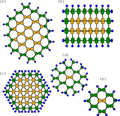
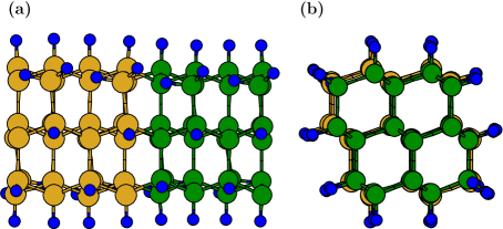
Besides “pure” Si and Ge nanowires, we also consider: coaxial Ge/Si nanowires with a Ge core and a Si overlayer; a nanowire with a periodic alternation of a few Ge and Si layers along the wire axis, forming a Ge/Si nanowire heterostructure; and three-layer-thin Si and Ge films, hydrogen-terminated on both sides, representing H-terminated (111) surfaces. The structures of the coaxial Ge/Si nanowires are shown in Fig. 1. The structures of the pure Si and Ge nanowires have the same initial geometry as those in Fig. 1, with all Ge and Si atoms replaced by either silicon or germanium. The geometry of the Ge/Si nanowire heterostructure is shown in Fig. 2, with a periodic unit along the axis formed by the alternation of four layers of Ge atoms and four layers of Si atoms. The atomic positions and lattice parameter of all nanowires and (111) surfaces were relaxed within the tolerances indicate above.


We now address the electronic structure of nanowires with one SDB defect per unit cell, obtained by removing a hydrogen atom from the nanowire surface and performing full ab initio structural optimizations. We ensure that the unit cells we use are large enough to decouple neighboring defects. For the majority of the nanowires, we consider SDB’s generated from GeH and SiH radicals, with the exception of wires with for which SiH2 (GeH2) radicals are considered [no SiH (GeH) radicals are present in this case]. Generally, we find that SDB Kohn-Sham eigenvalues are deep in the bandgap in the case of Si wires, and shallow (near the valence band edge) in the case of Ge wires. This is seen in Fig. 3, that shows the calculated band structures for the defective Si and Ge nanowires with nm, oriented along the (110) direction. The unit cells are 7.9 Å and 8.4 Å long along the axis, for the Si and Ge wires, respectively. Both band structures in Fig. 3 are essentially identical to those of the perfect wires (not shown), except for the appearance of a half-occupied nearly-dispersionless band in the gap. The small dispersions (0.03 eV for Si and 0.09 eV for Ge) are characteristics of localized SDB states. These features of the SDB level are common to all ten Si and Ge “pure” nanowires we consider.

From Janak’s theorem, janak , and the nearly linear dependence of the SDB eigenvalue on its occupation number , it follows that the eigenvalue of the neutral SDB state at the GGA, non-spin-polarized level, is a good approximation to the charge transition level footnotejanak . The latter is given by the value of the electronic chemical potential at which +1 and -1 charge states of a defect have equal formation energies. In Fig. 4 we show a comparison between the SDB neutral eigenvalue and the level, for the Si ( Å) and Ge ( Å) (112) wires. The straight lines for each charge state in Fig. 4 are , where is the supercell total energy for a nanowire with an SDB in charge state , is the Fermi level, and is the total energy for the perfect wire. The chemical potential for hydrogen, , is obtained from a Si (Ge) bulk and SiH4 (GeH4) molecule calculations. The eigenvalue of the neutral SDB state is plotted as a dashed vertical line, and is within 0.05 eV from the level for both Si and Ge. We obtained very similar results for Si and Ge wires oriented along the (110) direction. In the following, we present strong numerical arguments showing that the level of nanowire SDB’s is a common reference level among Si, Ge, and Ge/Si nanowires.


Let us first consider the electronic structure of the Ge/Si coaxial wires of Fig. 1 with an SDB state at the surface. Table 1 indicates the positions of the neutral SDB level relative to the valence band maximum, , and relative to the vacuum level, . The table shows that varies from a “shallow” value of 0.13 eV to a “deep” value of 0.50 eV, although the SDB’s are, in all cases, at the surface Si atoms of the coaxial wires. In contrast, is a common energy reference for all the SiH-terminated wires (i.e., all in Table 1 except for the wire with nm, which is SiH2-terminated).
| direction | (110) | (112) | (111) | (110) | (110) |
|---|---|---|---|---|---|
| Diameter | 23 Å | 19 Å | 17 Å | 15 Å | 12 Å |
| 1.05 | 1.40 | 1.52 | 1.35 | 1.67 | |
| -4.23 | -4.25 | -4.23 | -4.43 | -4.24 | |
| 0.13 | 0.15 | 0.29 | 0.44 | 0.50 |
To further investigate the nature of the SDB states, we performed a calculation for a Ge (110) nanowire with in which a GeH radical at the surface was replaced by a non-passivated Si atom, forming a Ge wire with an SDB at a substitutional Si atom at the surface. The band structures of this wire and of the corresponding one for a Ge wire with a “standard” Ge SDB are very similar to each other and to the one in Fig. 3(a). The SDB state at the Ge atom is at , while the SDB state at the Si atom is at . The same is observed for a Si (110) nanowire with in which a SiH radical at the surface is replaced by a non-passivated Ge atom: in this case, the SDB state at the Ge atom is at and the SDB state at the Si atom is at . These two cases demonstrate that the positions of the band edges relative to the SDB level are weakly dependent (within 0.15 eV) on the atomic species where the SDB is located, but strongly dependent on the electronic structure of the wire as a whole.
Our third numerical argument in favor of the universality of the SDB state is based on a Ge/Si heterostructure nanowire, shown in Fig. 2. We performed two separate calculations for SDB’s in this wire. In the first one, a hydrogen atom is removed from a Si surface atom. In the second one, we removed a hydrogen atom from a Ge surface atom. In both cases we placed the dangling bond as far as possible from the Ge/Si interface. Again, a striking resemblance is observed in both band structures: the SDB level at the Ge atom is at eV while at the Si atom it is at eV.

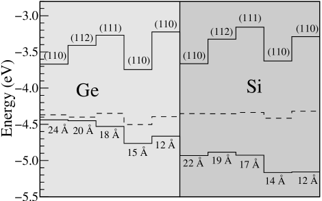
Given the above arguments, the level of the nanowire SDB’s (or, likewise, its Kohn-Sham eigenvalue in GGA or LDA approximations) should be a common reference level among Si, Ge, and Ge/Si nanowires, and could be used, for instance, to predict band-lineups in nanowire junctions footnote2 ; hannon and heterostructures. This is demonstrated in Fig. 5 where the calculated band edges (relative to the vacuum level footnote3 ) of all pure Si and Ge wires are shown together with the eigenvalues of the SDB states. Figure 5 shows that the SDB is a common energy level among the nanowires. The similarity of the is even stronger if we remove from the comparison the SiH2- and GeH2-terminated nanowires (the ones with diameters of 1.4 and 1.5 nm, respectively). By doing that, all values fall in a narrow range from eV to eV.
We also performed calculations for SDB’s on H-terminated Si and Ge (111) surfaces. We obtained eV (relative to the vacuum level) for the SDB on a Si surface, consistent with our results for the Si nanowires. For the SDB on a Ge surface, we find a resonant within the uppermost valence band, consistent with the fact that the top of the valence band 4.26 eV is above the nanowire values. In the case of the calculated Ge nanowires, Fig. 5 shows that is always below -4.4 eV (and therefore below ), with a a clear trend of increasing with diameter . This indicates that the values in Ge nanowires are downshifted in energy relative to the surface value due to quantum confinement. Therefore, for some diameter (larger than the ones considered in this work) there will be a transition between localized and resonant , with large-diameter Ge wires presenting a resonant . This is consistent with recent experimental results lou showing that large-diameter Si-covered Ge wires are intrinsically p-type.
Why should the SDB’s be a common energy reference? Previously, it has been proposed that both in the case of transition-metal impurities tersoff2 , and of interstitial-hydrogen impurities naturevw03 , the common energy reference is tied to an average dangling-bond energy which would be independent of the host material. This proposal has never been directly verified from first principles calculations, possibly because isolated dangling bonds are too reactive in bulk point defects. We argue that a surface dangling bond resulting from the removal of a hydrogen atom from a surface GeH or SiH radical should be a good realization of an ideal, unreconstructed dangling bond, as the surface Si or Ge atom with an SDB is bound to three saturated bulk-like atoms, with bond angles () and lengths () that are very similar to the defectless wire values ( 0.03 Å; , , and for Si, Ge and Ge/Si wires, respectively). Such small relaxations are indicative of small coupling between the SDB and the underlying bulk states.
To gain an even deeper insight into the physical origin of the SDB universality, let us consider this quantity in the limit of isolated atoms. We computed the atomic-limit using the same DFT approximations as in the nanowire calculations. In this limit, is defined as the average between the first-ionization potential and the electron affinity, computed for the atomic ground state. We obtained 4.39 eV for Si and 4.17 eV for Ge. This suggests that the universality is an atomic property. From similar atomic calculations for group III and V neighbors to Si and Ge, namely, Al, Ga, P, and As, we computed the atomic-limit average of the III-V compounds AlP, GaP, AlAs, and GaAs. We obtained 4.37 eV (AlP), 4.34 eV (GaP), 4.22 eV (AlAs), and 4.20 eV (GaAs), indicating that the applicability of the SDB common energy reference should go beyond Si and Ge.
In conclusion, ab initio calculations for hydrogen-terminated Si and Ge nanowires, nanowire heterostructures, and Si and Ge (111) surfaces, indicate that the charge transition levels of surface dangling bond states behave as a common energy reference among Si and Ge wires and Si/Ge heterostructures, at 4.3 0.1 eV below the vacuum level. Calculations of for isolated atoms indicate that this nearly constant value is a periodic-table atomic property.
Acknowledgements.
We acknowledge support from the Brazilian agencies CNPq, FAPEMIG, and Instituto do Milênio em Nanociências-MCT.References
- (1) J. Tersoff, Phys. Rev. B 30, 4874 (1984).
- (2) L. A. Ledebo and B. K. Ridley, J. Phys. C 15, L961 (1982).
- (3) M. J. Caldas, A. Fazzio, and A. Zunger, Appl. Phys. Lett. 45, 671 (1984).
- (4) J. Tersoff and W. A. Harrison, Phys. Rev. Lett. 58, 2367 (1987).
- (5) C. G. Van de Walle and J. Neugebauer, Nature 423, 626 (2003).
- (6) C. Kiliç and A. Zunger, Appl. Phys. Lett. 81, 73 (2002).
- (7) P. G. Piva et al., Nature 435, 658 (2005).
- (8) D. D. D. Ma et al., Science 299 , 1874 (2003).
- (9) W. Kohn, and L. J. Sham, Phys. Rev. 140, A1133 (1965).
- (10) J. P. Perdew, K. Burke, and M. Ernzerhof, Phys. Rev. Lett. 77, 3865 (1996).
- (11) N. Troullier, and J. L. Martins, Phys. Rev. B 43, 1993 (1991).
- (12) L. Kleinman, and D. M. Bylander, Phys. Rev. Lett. 48, 1425 (1982); X. Gonze, R. Stumpf, and M. Scheffler, Phys. Rev. B 44, 8503 (1991).
- (13) J. M. Soler et al., J. Phys.: Condens. Matter 14, 2745 (2002); P. Ordejón, E. Artacho, and J. M. Soler, Phys. Rev. B 53, R10441 (1996); D. Sánchez-Portal et al., Int. J. of Quantum Chem. 65, 453 (1997).
- (14) R. Kagimura, R. W. Nunes, and H. Chacham, Phys. Rev. Lett. 95, 115502 (2005).
- (15) J. F. Janak, Phys. Rev. B 18, 7165 (1978).
- (16) This result is only valid if is within the calculated bandgap. This applies to all our nanowire calculations.
- (17) Junctions made of Si nanowires with different diameters have been recently observed hannon .
- (18) J. B. Hannon et al., Nature 440, 69 (2006).
- (19) Unlike a bulk heterojunction, a nanowire heterojunction has a well-defined vacuum level. In the GGA or LDA approximations, it is given by the asymptote of the Kohn-Sham potential away from the nanowire axis, namely, E=0 . Due to the exponential decay of from the surface in GGA (or LDA) and to the finite range of the basis set, the Kohn-Sham eigenvalues converge rapidly with supercell size.
- (20) W. Lu, J. et al., Proc. Natl. Acad. Sci. 102, 10046 (2005).