noise as a probe for investigating band structure in graphene
Abstract
A distinctive feature of single layer graphene is the linearly dispersive energy bands, which in case of multilayer graphene become parabolic. Other than the quantum Hall effect, this distinction has been hard to capture in electron transport. Carrier mobility of graphene has been scrutinized, but many parallel scattering mechanisms often obscure its sensitivity to band structure. The flicker noise in graphene depends explicitly on its ability to screen local potential fluctuations. Here we show that the flicker noise is a sensitive probe to the band structure of graphene that vary differently with the carrier density for the linear and parabolic bands. Using devices of different genre, we find this difference to be robust against disorder in the presence or absence of substrate. Our results reveal the microscopic mechanism of noise in Graphene Field Effect Transistors (GraFET), and outline a simple portable method to separate the single from multi layered devices.
In a field-effect device, the flicker noise manifests in slow fluctuations in the drain-source current due to the fluctuations in the channel conductivity, . The flicker noise is often called the -noise because of its power spectral density, , where is frequency, and . The -noise has been studied extensively in metal-oxide field effect transistors (MOSFET), where the trapping and detrapping of charge at the channel-oxide interface represent a collection of two-state fluctuators correlated model_jayaraman . A wide distribution in the fluctuator switching rate leads to noise in these devices. Similar mechanism of noise have been assumed for carbon nanotube field-effect devices as well CNT_avouris , where the trapping events close to the nanotube-metallic lead Schottky barriers cause fluctuations in the effective gate voltage CNT_charge noise .
In spite of the close architectural similarity to MOSFETs or nanotube-based FETs, the microscopic understanding of noise in GraFETs is rather limited Avouris 1 ; atin PRL ; atin APL ; Charge noise ; Noise_Xu ; Noise_Balandin ; Noise_suspended . An augmented charge noise model charge_noise_IBM , developed in the context of carbon nanotubes, fails to describe the carrier density () dependence of noise in most single layer graphene (SLG) devices close to charge neutrality (the Dirac point) Avouris 1 ; atin APL . The model does not consider the graphene band structure explicitly, and hence fails to account for distinct noise behavior in SLG and bilayer (BLG) GraFET devices Avouris 1 ; atin PRL , which becomes more dramatic at lower temperatures (). The influence of quenched disorder, and related charge inhomogeneity martin , which are both very serious technological bottlenecks, are also not known. With emerging techniques of realizing graphene at commercial production scale, such as chemical vapor deposition on metals CVD_science or epitaxial growth on SiC SiC_Science1 , the behavior of noise at low carrier density, , where is the scale below which charge distribution in graphene becomes inhomogeneous, needs to be addressed. In this work we explore the possibility of a global framework within which flicker noise in GraFET devices of different genre CVD_science ; SiC_Science1 ; GNR ; suspended graphene and substrates high K ; graphene_BN ; mica nature can be understood and analyzed.
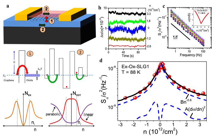
We consider the generic GraFET structure in the schematic of Fig. 1a, where the local environment of the graphene film consists of the underlying insulating substrate, and surface adsorbates (or top gate dielectric, if any). Focussing on the noise that arises due to fluctuating charge distribution (FCD) around the graphene film, two processes are identified: (1) Exchange of charge between graphene and its environment, for example through trapping-detrapping process, which involves time-dependent changes in . This causes a charge exchange noise, through correlated number and mobility () fluctuations correlated model_jayaraman . (2) The second process consists of a slow rearrangement of charge within the local environment of graphene, for example, random migration of trapped charges within the substrate or surface adsorbates (Process 2 in the schematic in Fig. 1a), and referred as configuration noise (). This process alters the disorder landscape due to Coulomb potential from trapped charges leading to random fluctuations in the scattering cross-section (). Within a “local interference” framework Pelz , , where is the screened Coulomb potential of the trapped charge. Thus at large , , where is the mean scattering length Pelz , where is determined by the -dependence of and , and hence is sensitive to the nature of graphene band structure. Assuming Boltzman transport in Thomas-Fermi screening, the total normalized noise power spectral density can be written as (see supplementary material for full derivation),
| (1) |
To the leading order the parameters and are independent of irrespective of the band structure, but depend on . The function for , while for , the charge distribution in graphene disintegrates into electron-hole puddles martin , and noise is determined by changes in the percolation network and weak links between puddles. In this regime, we take constant (see schematic in Fig. 1a). In analyzing the noise data, the parameters and were kept as fitting parameters, and was obtained from the data. Due to particle-hole asymmetry gordon the electron and hole-doped regimes were fitted separately phonon_avouris .
We have used seven different types of graphene field effect devices in our experiments which include exfoliated single and multilayer graphene on oxide substrate, freely suspended single layer graphene, and chemical vapor deposition (CVD)-grown graphene on Si2 (see Table 1 for details). Graphene flakes were prepared on nm SiO2 on doped silicon substrate (the backgate) by micromechanical exfoliation of natural graphite (NGS Naturgraphit GmbH). In all the cases, we have used RCA cleaning of the substrate, and standard electron beam lithography technique followed by thermal evaporation of 40-50 nm gold () to fabricate the devices. For suspended graphene transistor, nm thick gold electrodes were made, followed by etching of the underneath oxide by buffered HF solution for minutes. Finally, the devices were released in a critical point dryer. No current annealing or Ar/H2 annealing was used in our experiments to remove the acrylic residues in any of the devices. To avoid large electrostatic force, only small range of gate voltage was scanned, corresponding to cm-2. The CVD-graphene was grown by thermal decomposition of methane on m thick copper foil at C. Methane was introduced into the chamber at a rate of sccm and a pressure of Torr for a growth time of minutes after which the chamber was cooled down to room temperature. The susbsequent processes involved PMMA coating, dissolving copper foil with Ferric Chloride ( g FeCl3/ ml conc. HCl/ ml de-ionized water), transfer onto the Si/SiO2 substrate, coating a second PMMA layer, and finally cleaning with acetone/IPA. Noise in the graphene devices were measured in low-frequency ac four- and two-probe methods in a high vacuum environment. See Ref arindam_arxiv for details. The excitation was below 50 A to avoid heating and other non-linearities, and verified by quadratic excitation dependence of voltage/current noise at a fixed resistance . The background noise was measured simultaneously, and subtracted from the total noise.
The FCD model was first examined with an exfoliated SLG device (Ex-Ox-SLG1). The inset of Fig. 1c shows to vary linearly at low , indicating scattering from charged impurities. The normalized fluctuations, , peak at the Dirac point, as evident from the time traces in Fig. 1b. We find at all (Fig. 1c). Both four- and two-probe measurements yielded same results, indicating negligible contribution from contact noise. decreases monotonically as is increased on both electron and hole doped sides (Fig. 1d). Fitting Eq. 1, shown in solid dark line, yields excellent agreement. Two key factors can be noted here. First, exceeds at all , particularly at lower (dashed lines in Fig. 1d). Indeed, the peak in at the Dirac point can be attributed to larger configurational noise, i.e. enhanced sensitivity of graphene to alteration in disorder landscape, with charge noise being minimal since varies weakly with in this regime. Second, the fit yields , which was found to be generic to other SLG devices as well (see also Fig. 4a). Within the Thomas-Fermi approximation, for SLG ( is the Fermi wave vector) sdsarma_BLG . Taking , where for both screened Coulomb sdsarma_BLG and interface phonon scattering phonon_natnano ; phonon_avouris in graphene, we get , as indeed observed.
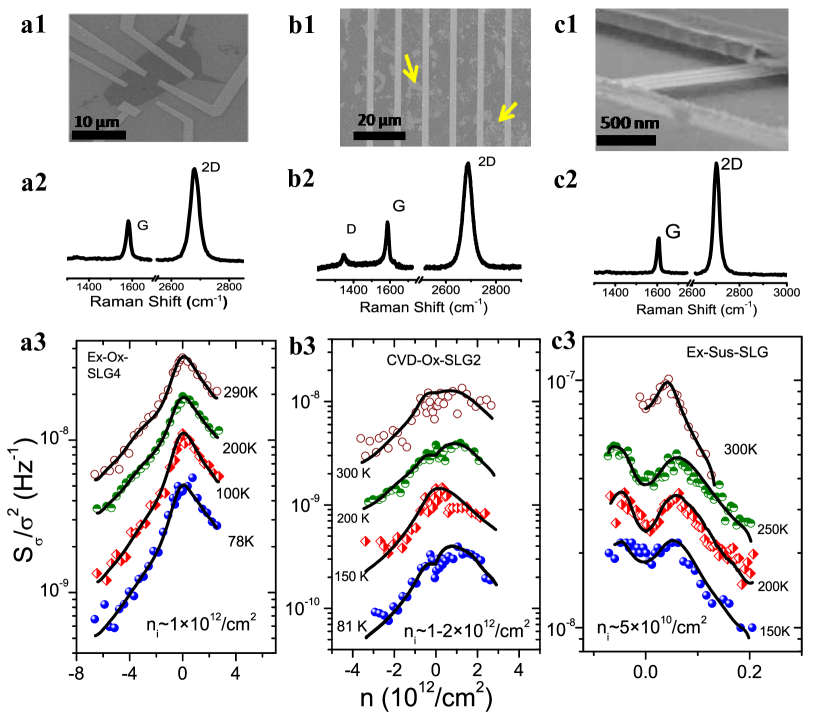
The validity of the analysis was then confirmed to be robust with SLG against varying levels of quenched disorder. Here, the noise in three SLG devices obtained by, (1) mechanical exfoliation on SiO2 substrate (Ex-Ox-SLG4, Fig. 2a1-a3), (2) chemical vapor deposition (Cvd-Ox-SLG2, Fig. 2b1-b3), and (3) mechanically exfoliated suspended single layer graphene (Ex-Sus-SLG, Fig. 2c1-c3), are compared. For Cvd-Ox-SLG2, the transfer process onto the SiO2/Si substrate introduce considerable disorder, both structural (ruptures/voids) and foreign charged/uncharged residues (see the electron micrograph and the disorder peak in the Raman spectrum in Fig. 2b2), resulting in rather poor cm2/Vs (see Table I). In spite of this, we find overall similarity in the behavior of in all SLG devices on oxide substrate (including Ex-Ox-SLG1 in Fig. 1d). The magnitude of ( cm-2) in Cvd-Ox-SLG2 is significantly larger than typical in exfoliated SLG devices, confirming a greater inhomogeniety in the former. In all cases Eq. 1 provides an excellent fit to the data with (see Fig. 4a). For Cvd-Ox-SLG2, significant electron-hole asymmetry due to impurity scattering leads to asymmetric noise behavior. It is remarkable that in spite of higher level of structural disorder, noise in CVD-grown graphene continues to be dominated by fluctuating charge distribution, indicating that migration of structural disorder is mostly frozen well up to the room temperature.
The noise behavior is qualitatively different in the low disorder limit, as indicated by the suspended SLG device Ex-Sus-SLG (Fig. 2c1-c3). Measurements were performed on as-fabricated device, which was mildly electron doped due to surface residues and contamination (see Table I). The noise magnitude at Hz is shown in Fig. 2c3, which was considerably lower than the other SLG devices when normalized by device size and low operating (see also Fig. 4b). Intriguingly, the noise in Ex-Sus-SLG varies nonmonotonically with at all . In spite of this difference, fitting Eq. 1 gives excellent agreement, albeit with a much greater contribution from which results in the non monotonic behavior. We believe the observed noise in our suspended graphene to be due to residual surface contamination, in particular the residues of the electron beam resist (PMMA). The analysis also confirms to be negative which approaches near room temperature (Fig. 4a) due to a nearly constant from competing scattering processes.
| Device | Growth | Layer | Substrate | Device area (LW)111both dimensions in m | Mobility 222in cm2/V.s |
|---|---|---|---|---|---|
| Ex-Ox-SLG1 | Exfoliation | 1 | SiO2 | ||
| Ex-Ox-SLG4 | Exfoliation | 1 | SiO2 | ||
| Ex-Ox-BLG2 | Exfoliation | 2 | SiO2 | ||
| Cvd-Ox-SLG2 | CVD | 1 | SiO2 | ||
| Ex-Sus-SLG | Exfoliation | 1 | Suspended | ||
| Ex-Ox-FLG | Exfoliation | 3-4 | SiO2 | ||
| Ex-Ox-MLG | Exfoliation | 14-15 | SiO2 |
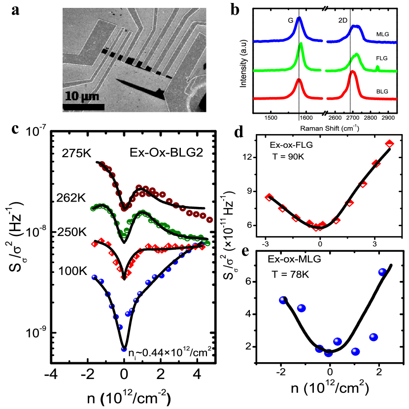
Noise measurements on BLG led to a rather striking result. Fig. 3a-c show a micrograph, Raman spectrum, and -dependence of noise in an exfoliated BLG device (Ex-Ox-BLG2) on identically treated SiO2/Si substrates. No top gate, H2/Ar treatment, or current annealing was used. The intrinsic electron-doping restricted us only to the electron-doped region for detailed -noise measurements. in BLG device clearly behaves very differently from the SLG devices in Fig. 2. At low ( K), increases monotonically with , in agreement to our earlier results atin PRL , but becomes nonmonotonic at higher , similar to the results reported by Heller et al. Charge noise . Eq. 1 can however be fitted rather well to the BLG noise data over the entire range of albeit with a positive for all . We find up to (Fig. 4a). We suggest positive magnitude of to be due to the parabolic energy bands in BLG. Quantitatively, within the Thomas-Fermi approximation, is independent of for BLG to the leading order sdsarma_BLG , resulting in , i.e. . Close to room temperature, varies weakly with , possibly due to competing scattering from the longitudinal acoustic phonons phonon_natnano ; phonon_avouris , causing the nonmonotonicity of to be visible in the -dependence of total noise. We have also measured flicker noise in few-layer (FLG, layers, Fig. 3d) and many-layer (MLG, layer, Fig. 3e) GraFET devices as well. Eq. 1 provides good fit to noise in these systems with a small positive arising from the parabolic bands at low energies.
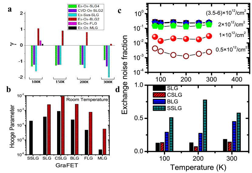
In essence, Graphene displays both trapping-detrapping-like noise in MOSFET (exchange noise) and that from changes in extended structural disorder as in disordered metal films (configuration noise). The origin of both in this case is a fluctuating charge distribution, where the sensitivity of configurational component (more specifically, ) to band structure allows one to distinguish between the linear and parabolic bands(Fig. 4a). In fact, we find the configurational component to dominate in most devices and densities, as indicated in Fig. 4c and 4d, but strongly depends on the quality of the substrate surface, roughness, nature of dielectric, operating etc. This can vary widely from one device to the other, helping us to understand the apparently different experimental results on GraFET noise reported from different research groups Avouris 1 ; atin PRL ; atin APL ; Charge noise ; Noise_Xu ; Noise_Balandin ; Noise_suspended . Not surprisingly, the exchange noise is maximum in the suspended devices (Fig. 4d), where the discontinuous layer of surface residues leaves very little room for the trapped charges to redistribute.
Fig. 4b summarizes normalized noise levels in different designs of GraFET. The comparison is made in terms of the phenomenological Hooge parameter , defined as where is the area of the graphene film between voltage leads. At all , the substrated SLG devices, exfoliated or CVD-grown, are most noisy, whereas suspended SLG and thicker graphene systems are nearly hundred times quieter. At room temperature, and even on a substrate, can be in FLG and MLG devices atin APL , which is among the lowest known for metal or semiconductor nanostructures. The extreme low noise in these systems is due to strong screening by the lower layers, which also affects the gating ability, limiting their usefulness in active electronics, but make them suitable as interconnects.
Acknowledgement We acknowledge the Department of Science and Technology (DST) for a funded project. ANP, SG and VK thank CSIR for financial support.
References
- (1) R. Jayaraman, C. G. Sodini, IEEE Trans. on Electron Devices 36, 1773 (1989).
- (2) Y.-M. Lin, J. Appenzeller, J. Knoch, Z. H. Chen, P. Avouris, Nano Lett. 6, 930 (2006).
- (3) J. Männik, I. Heller, A. M. Janssens, S. G. Lemay, C. Dekker, Nano Lett. 8, 685 (2008).
- (4) Y. -M. Lin and P. Avouris, Nano Lett. 8, 2119 (2008).
- (5) A. N. Pal and A. Ghosh, Phys. Rev. Lett. 102, 126805 (2009).
- (6) A. N. Pal and A. Ghosh, Appl. Phys. Lett. 95, 082105 (2009).
- (7) I. Heller et al., Nano Lett. 10, 1563 (2010).
- (8) G. Xu et al., Nano Lett. 10, 3312 (2010).
- (9) S. Rumyantsev et al., arXiv:condmat/1008.2990v1.
- (10) Z. Cheng et al., Nano Lett. 10, 1864 (2010).
- (11) J. Tersoff, Nano Lett. 7, 194 (2007).
- (12) J. Martin et al., Nat. Phys. 4, 144 (2008).
- (13) X. Li et al., Science 324, 1312 (2009).
- (14) C. Berger et al., Science 312, 1191 (2006).
- (15) J. Cai et al., Nature 466, 470 (2010).
- (16) K. I. Bolotin et al., Solid State Commun. 146, 351 (2008).
- (17) L. A. Ponomarenko et al., Phys. Rev. Lett. 102, 206603 (2009).
- (18) C. H. Lui et al., Nature 462, 339 (2009).
- (19) L. Ci et al., Nat. Mater. 9, 430 (2010).
- (20) J. Pelz and J. Clarke, Phys. Rev. B 36, 4479 (1987).
- (21) B. Huard, N. Stander, J. A. Sulpizio, D. Goldhaber-Gordon, Phys. Rev. B 78, 121402(R) (2008).
- (22) W. Zhu, V. Perebeinos, M. Freitag, P. Avouris, Phys. Rev. B 80, 235402 (2009).
- (23) A. Ghosh et al., arXiv:condmat/0402130.
- (24) S. Adam and S. Das Sarma, Phys. Rev. B 77, 115436 (2008).
- (25) J-H., Chen, C. Jang, S. Xiao, M. Ishigami, M. S. Fuhrer, Nature Nanotech. 3, 206 (2008).