Role of linear and cubic terms for the drift-induced Dresselhaus spin-orbit splitting in a two-dimensional electron gas
Abstract
The Dresselhaus spin-orbit interaction (SOI) of a series of two-dimensional electron gases (2DEGs) hosted in GaAs/AlGaAs and InGaAs/GaAs (001) quantum wells (QWs) is measured by monitoring the precession frequency of the spins as a function of an in-plane electric field. The measured spin-orbit-induced spin-splitting is linear in the drift velocity, even in the regime where the cubic Dresselhaus SOI is important. We relate the measured splitting to the Dresselhaus coupling parameter , the QW confinement, the Fermi wavenumber and to strain effects. From this, is determined quantitatively, including its sign.
The spin-orbit interaction (SOI) couples electron spins to the orbital motion. In semiconductor quantum structures, SOI often limits the spin lifetime and therefore needs to be minimized when spins are to be used for processing or storing information. On the other hand, SOI has the potential to locally control spins by electrical means.Datta1990 The reliable manipulation of spins is crucial for spin-based quantum computing Loss1998 and for spintronic applications Wolf2001 . For a two-dimensional electron gas (2DEG) hosted in a semiconductor with zinc-blende structure, there are two main sources for SOI: The Rashba SOI Bychkov1984 and the Dresselhaus SOI Dresselhaus1955 . The Dresselhaus SOI is a bulk property as it arises form the inversion asymmetry of the crystal. The resulting spin splitting is cubic in the components of the electron wave vector . In a 2DEG, the quantum confinement along the growth direction leads to bound states with the expectation value and a quantized value for . This constriction of the orbital motion modifies the spin splitting in terms of the in-plane momentum components: In addition to a cubic dependence, there is also a term proportional to that is linear in the components of the in-plane wave vector .Dyakonov1986 The strength of both terms is given by the Dresselhaus coupling constant . The value of has been measured quantitatively with various techniques, including Raman scattering,Jusserand1992 magneto transport,Dresselhaus1992 ; Miller2003 ; Krich2007 spin-dephasing measurements Marushchak1983 and spin-grating measurements.Koralek2009 These techniques probe states selectively at the Fermi surface, and the spin splitting is directly related to the Fermi wave number . In contrast, drift-related experiments Kalevich1990 ; Kato2004 ; Meier2007 ; Wilamowski2007 ; Studer2009 involve a small displacement of the Fermi surface and lead to a drift-induced spin splitting that is proportional to and a direction dependence that can be described by an effective magnetic field . This field is composed of a Rashba component and a Dresselhaus component , which have different symmetry with respect to . Quantitative values, including the absolute sign, for both Rashba and Dresselhaus SOI can be obtained by monitoring the coherent spin precession in an external magnetic field .Kato2004 ; Meier2007 ; Studer2009
In this work, we investigate the interplay of the linear and cubic terms of the Dresselhaus SOI of a 2DEG as manifested in measurements of versus . The cubic term becomes important for , and it has been suggested that in this regime has a cubic dependence on .Meier2007 ; Chernyshov2009 ; Norman2010 ; Bernevig2005 Here we show that depends linearly on (), even in the regime of . A central aspect of this work is to discuss how the linear and the cubic Dresselhaus SOI terms contribute to by deriving an explicit expression for from the Dresselhaus Hamiltonian . The calculations show that the slope of versus is decreased by the cubic term, and changes its sign when . We experimentally studied samples made of two material systems displaying different Fermi and confinement energies, namely 10-nm and 20-nm-wide InGaAs/GaAs QWs, and 15-nm-wide GaAs/AlGaAs QWs. A linear dependence of on is measured in all cases of . Cubic contributions are small for the GaAs/AlGaAs QWs and we find eVÅ3. For the InGaAs/GaAs QWs, cubic contributions significantly modify the slope of versus . In addition, a more detailed analysis of the slope provides evidence of a strain-induced contribution that has the same symmetry as the linear Dresselhaus SOI.
The paper is organized as follows: First we lay out the theoretical framework and define the Dresselhaus SOI and the coordinate system, the basis for an unambiguous definition of the sign of . Then, we derive the linear dependence of versus . Next, we present experimental data for a series of samples in which the importance of the cubic term varies, and finally discuss the results with respect to the theory developed.
I Dresselhaus spin-splitting
Dresselhaus SOI for a 2DEG is described here in the coordinate system () defined by the cubic crystallographic axes . These directions are specified in a GaAs primitive cell, with the cation (Ga) residing at (0, 0, 0) and the anion (As) located at (, , ). This is the same convention as used by wafer manufacturers, and is compatible with the literature on direction-selective etching processes.Shaw1981 ; Adachi1983 In contrast, in some theoretical works,Cardona1986 ; Cardona1988 the anion is placed at the origin of the coordinate system. This specification is important for an unambiguous definition of the Dresselhaus parameter because the exchange of cation and anion involves a change in the sign of .Cardona1986 In the following, we discuss (001)-grown QWs with one occupied subband and the Dresselhaus Hamiltionian
| (1) |
where is the quantum-mechanical expectation value of with respect to the envelope wave function of the occupied subband, and are the Pauli matrices. In this notation, two terms show up: A term that is linear in the in-plane momentum components and a term that is cubic. To study the interplay of these two terms, we compare their magnitude for on the Fermi surface, i.e. for : The ratios and have an upper limit of and are zero for certain orientations of . Therefore, the linear term is dominant in the case of strong confinement, i.e. for . In terms of the QW sheet density and the QW width , the importance of cubic terms scales with the product , because and .
For the further discussion, it is convenient to express as a spin-splitting induced by an effective magnetic field that depends on the electron wave vector :
| (2) |
Here is Bohr’s magneton of the free electron with mass , and is the effective -factor in the semiconductor QW. and are the two eigenvalues of for a given . In our coordinate system and in correspondence with Eq. (1), we separate the linear and cubic contributions according to
| (3) |
| (4) |
| (5) |
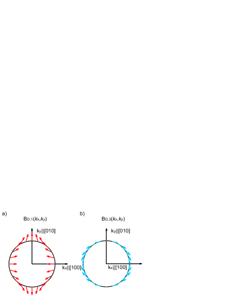
The different symmetries of the two contributions are illustrated in Fig. 1 by plotting the vector fields and for a specific . The magnitude of does not depend on the direction of , whereas is maximal for along the and direction, and zero along and .
So far, we have only considered Dresselhaus SOI. Other sources of SOI include structure inversion asymmetry (Rashba SOI) and strain. Their corresponding spin splitting can also be expressed as an effective magnetic field. In case of the Rashba SOI, this field can be separated from the Dresselhaus SOI because of its different symmetry in . However, biaxial strain gives rise to a spin splitting that has the same symmetry as the linear Dresselhaus SOI [first term in Eq. (1)]. Its effective magnetic field can be expressed asMeier1984 ; Bernevig2005
| (6) |
Here, , where is a material parameter and is the strain tensor. Such a component has been observed in InGaAs epilayers grown on GaAs, where it can be stronger than the Dresselhaus contribution.Kato2004 To our knowledge, there is no systematic work describing the strain contribution in -doped QWs and only few experimental studies.Studenikin2003 For completeness and cross-referencing, we introduce the Rashba coupling constant and the effective magnetic field induced by Rashba SOI:
| (7) |
II Calculation of the drift-induced spin splitting
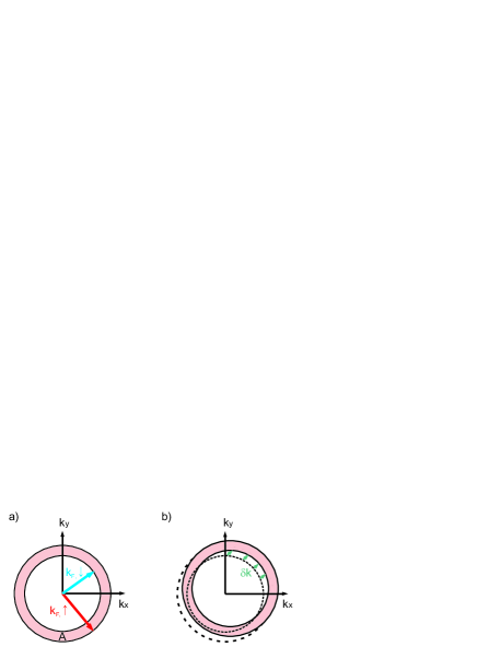
The effective magnetic field discussed in the previous section affects individual electron spins. Drift-related experiments involve all states near the Fermi surface, and a corresponding average of is observed. In our experiment, only a part of the 2DEG is spin polarized, and we measure the coherent precession of those spins in their corresponding field . The initial spin polarization is oriented along (denoted as ”spin up” polarization), and can be described by two Fermi wave numbers and : Spin-up (spin-down) states are homogeneously filled up to () at 0 K [Fig. 2(a)]. The spin polarization is given as .
To connect with the spin-precession frequency measured in the experiment, we average over the spin-polarized area [shaded gray (red) in Fig. 2(a)]. This approach is reasonable for nonselective optical probe techniques and for fast electron momentum scattering. In equilibrium, the average over is obviously zero for the rotationally symmetric fields and . However, if the 2DEG is exposed to an in-plane electric field , the spin-polarized states are shifted from the equilibrium position in the direction of the drift wave vector [Fig. 2(b)]. Note that points in the opposite direction than because the electron mobility is positive by definition and corresponds to electrons with a negative charge. Using polar coordinates , the average over the shifted area is given by the integral
| (8) |
.
This averaging transforms and into a drift field that expresses the average field experienced by the polarized electron spins. The dominant term in is linear in , and third-order terms in are unimportant for and . We note that the terms proportional to and originate from , i.e., the cubic Dresselhaus term affects in linear order. The symmetry of is the same as that of , and the cubic terms do change neither this symmetry nor the linearity in . For small spin polarization, we can approximate and in Eq. (8) by the Fermi wave number of the unpolarized spins. In a previous publication the influence of the cubic Dresselhaus term has been underestimated by a factor of two because of the assumption of a high spin polarization.Studer2009 Using the above described simplification, reasonable for a typical experiment, we define the drift-field Dresselhaus coefficient
The importance of Eq. (10) is based on the direct experimental accessibility of , whereas the parameter has to be calculated from , , and . Temperature broadening leads to an increase of the cubic Dresselhaus contributions in Eq. 9 that becomes significant if is comparable to .Weng2004 In our measurements this correction is below 10 %.
III Measurement of the Dresselhaus SOI
We investigate Si-doped -type material systems, namely epitaxially grown GaAs/AlGaAs QWs and InGaAs/GaAs QWs. All QWs have been grown along [001]. The InGaAs/GaAs QWs are single QWs, whereas the GaAs/AlGaAs samples consist of a series of 14 equivalent QWs. Narrow GaAs/AlGaAs QWs are suited for a reliable determination of the Dresselhaus coupling constant , because GaAs/AlGaAs is a nearly strain-free system, and cubic contribution are small for narrow QWs. InGaAs/GaAs QWs with less confinement and large electron density are used to study cubic Dresselhaus SOI and to test the consistency with a strain-induced contribution. Table 1 summarizes the parameters of all QWs that were used.
All optical measurements have been done at elevated temperature of 40 K, to preclude nuclear spin effects. The sheet carrier density of the 2DEGs was measured separately in a perpendicular magnetic field, using both Hall and Shubnikov–de Haas measurements. Both methods yield equivalent at 1.6 K. The mobility was then calculated from the four-terminal resistance. A quantity that can not be accessed in the experiment is . In previous publications, was used, where is the width of the QW.Studer2009 ; Koralek2009 This approximation is based on a square potential QW with an infinitely high confinement potential in the direction. Note that this is an appropriate estimate only for QWs with a very large conduction-band offset. To improve the accuracy of the experimentally determined value for , we have used a one-dimensional Poisson and Schrödinger equation solver 000Calculations were done with the Nextnano3 software version 2004-Aug-24 to calculate the envelope wave function of the ground state , and then numerically determined the expectation value . The numerical approach yields m-2 for a 15-nm-broad GaAs/Al.3Ga.7As QW. This is considerably less than for an infinite barrier [ m-2], because of leakage of the wave function into the barrier region and electron screening.
| QW/host material | |||||||||
|---|---|---|---|---|---|---|---|---|---|
| no. | (number of wells) | (nm) | (m2/Vs) | (m | (m-2) | (m-2) | (eVm) | (eVm3) | (eVm) |
| 1 | In.10Ga.90As/GaAs (1 ) | 20 | 1.3 | 0.95 | 3.2 | 5.2 | 0.2 | -7.5 | 0.7 |
| 2 | In.12Ga.88As/GaAs (1 ) | 10 | 4.5 | 2.25 | 2.8 | 4.5 | 1.3 | -7.5 | 1.7 |
| 3 | GaAs/Al.3Ga.7As (14 ) | 15 | 51 | 2.5 | 0.74 | 1.2 | 1.7 | -8.0 | 2.0 |
| 4 | GaAs/Al.3Ga.7As (14 ) | 15 | 36 | 2.5 | 0.86 | 1.4 | 1.0 | -4.7 | 1.2 |
| 5 | GaAs/Al.3Ga.7As (14 ) | 15 | 24 | 2.5 | 0.99 | 1.6 | 1.0 | -5 | 1.3 |
To apply an in-plane electric drift field in a specific direction, a mesa structure is etched into the substrates hosting the 2DEG to form 100-m or 150-m-wide conductive channels. The geometry of the mesa structure is cross-shaped for samples 1 and 3, whereas unidirectional mesa bars were used for the other samples. The electric field is inhomogeneous in the center of the cross-shaped mesa, a fact that has been accounted for in the evaluation.Studer2009 Ohmic contacts to the buried channel are subsequently fabricated by standard AuGe diffusion. In the experiment, a small spin-polarization of the electron spins in the conduction band of the QW is generated by a circularly polarized pump-pulse generated by a mode-locked Ti:sapphire laser. The energy per area of the pump pulses was kept below 210-2 Jm-2 for sample 1 and 2, and below 410-3 Jm-2 for samples 3-5. These small intensities ensure that the number of electron-hole pairs that are excited per QW is much smaller than the number of electrons already in the QW. Therefore, only a small fraction of the electrons become spin-polarized by the pump pulse.
The experiment then monitors, in the time domain, the coherent precession of electron spins in an external magnetic field using time-resolved Kerr rotation (TRKR) or time-resolved Faraday rotation (TRFR).Meier2007 The spin precession frequency is given by
| (11) |
is applied in the plane of the QW, and SOI-induced contributions to the spin splitting become visible as an -field-dependent change of given by . The observation of several periods of spin precession during the spin lifetime is required to precisely determine and thus . This is made possible by exposing the sample to . In bulk GaAs, where the spin lifetime is much longer than in QWs, coherent spin precession about has been observed at .Kato2004
For our experiments, , and therefore can be approximated by
| (12) |
i.e. is proportional to the projection of along the direction of the external field. By selecting the orientation of with respect to , the contributions with Dresselhaus symmetry, , can be separated from contributions having another symmetry. We used two different methods for this separation:
| , with | ||||
| , with |
For (I), is recorded for two orientations of , 222 and are either parallel or antiparallel for this set of directions. and the sum of these two measurements yields the Dresselhaus contribution .Meier2007 For (II), is a direct measure of the Dresselhaus contribution ,Meier2007 333 for this set of directions, and . i.e.,
| (13) |
As an example, data from sample 4 is shown where we used method II to directly see the influence of the Dresselhaus SOI. Figure 3(a) shows experimental TRKR traces measured with =0.93 T applied along . The factor is obtained from the trace at . Also the data for along and along have been plotted. In this configuration, increases for along .
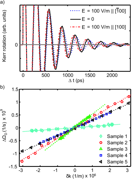
As a central finding, we show that depends linearly on the drift wave-number [Fig. 3(b)]. This is supported by experimental data from various samples (listed in Table 1). For sample 1 and 2, has been obtained using method (I), and for sample 3, 4 and 5, we used method (II). According to Eqs. (10) and (13), the slope of the fit in Fig. 3(b) is given by . The sign of is determined from the direction of with respect to : For example, for along (), points along and, according to Eq. (10), points along for and . From Eq. (12), we see that is negative if is applied along . Therefore, the sign of must be positive for the data shown in Fig. 3(a). As seen from Table 1, we find for all samples investigated.
IV Discussion
First, we will discuss the results for GaAs/AlGaAs and compare with the literature values. Second, we present the results for InGaAs/GaAs, for which we expect a significant contribution to SOI from third-order terms and strain. Finally, we compare the sign of we obtained with the results of other experimental work.
As GaAs/AlGaAs grows nearly strain-free, we assume and calculate directly from the measured using Eq. (9) and the values of and (Table 1). For , we find values in the range of -4 to -8 eVÅ3. These values are smaller than previously reported for GaAs/AlGaAs QWs Jusserand1995 ; Jusserand1992 ; Dresselhaus1992 ; Miller2003 and GaAs bulk crystals,Marushchak1983 where covers a rather wide range of 11-27 eVÅ3. Recent results from spin-grating measurements yield eVÅ3, assuming m-2.Koralek2009 For these QWs, our simulations suggest m-2, which corresponds to eVÅ3. A similar result of eVÅ3 was found for a quantum dot hosted in an AlGaAs/GaAs heterostructure.Krich2007 Measurements of spin-orbit-induced spin precession at Leyland2007 and of factor anisotropyEldridge2010B yield values of between 4 and 10 eVÅ3.
Results from theoretical calculations are in the range of eVÅ3 (see supplementary notes of Ref. Krich2007, ).
There are several possibilities for an error in the experimental value for . In particular, a systematic underestimation of could result from a reduction of the drift wave-number under optical illumination. The electric field and therefore have been determined from the four-terminal resistance measured simultaneously with the TRKR (TRFR). The pump pulse locally creates electron-hole pairs that initially screen the applied electric field. This effect can be reduced by using pump pulses with smaller intensities. Indeed, we observe a small dependence of upon the pump power. For sample 5, increases to about 1.210-13 eVm if the pump intensity is decreased by a factor of 8 (reaching 510-4Jm-2). We have not observed a persistent photoeffect: The average electron density as determined from both Hall and Shubnikov–de Haas measurements did not change significantly upon illumination with a light-emitting diode.
To investigate the effect of cubic Dresselhaus SOI and to quantify the importance of cubic terms compared with that of linear terms, we have chosen samples with large and small , such that (sample 1). For this sample, we find , which at first sight is surprising because is expected to change sign for if [Eq. (9)]. The positive sign can be explained if strain affects the SOI. For simplicity, we assume that samples 1 and 2 have the same and . With the values of and listed in table 1, we solve the set of equations given by Eq. (9) with the two unknowns and . As a result we obtain eVm and eVÅ3. This value for is in rather good agreement with the results for the GaAs/AlGaAs QWs and suggests that 2D structures can exhibit strain-induced spin-splitting with magnitudes comparable to the linear Dresselhaus SOI ( eVm for sample 1). In this analysis, the biaxial strain component directly affects the resulting , and further more systematic investigations are needed to obtain a more precise value for in InGaAs/GaAs QWs.
In our measurements, the sign of is negative for all samples. Some care has to be taken to determine the sign of . We have experimentally verified the sign of the magnetic field in our lab. Moreover, the sign is based on the assumption that and that the drift direction is the opposite direction of , i.e. . We have kept track of the crystallographic direction indicated by the wafer manufacturer during processing and double checked with a selective etching test.Shaw1981 ; Adachi1983 The often cited positive sign of is specified in an As-based coordinate system, which translates to a negative sign in a Ga-based system.Cardona1986
In Ref. Riechert1984 the sign of for a GaAs bulk crystal has been measured by analyzing the phase that an electron spin acquires during traveling. A positive has been obtained in an As-based coordinate system, in agreement with our result. The sign of can also be compared with experiments that only determine the sign of the ratio if the sign of is known. From previous measurements on a parabolic QW with back and front gates,Studer2009PRL the sign of has been determined to be positive for an electric field pointing along the growth direction . From , it follows that is positive for . This is in agreement with Ref. Frolov2009, : Using a ballistic spin resonance experiment, a negative sign of has been determined in the heterostructure investigated with along . It is also compatible with Ref. Larionov2008, : is determined from the spin-dephasing anisotropy and becomes negative for bias voltages larger than 1.2 V. In that experiment, is defined as ( in our definition), and a positive bias means a negative voltage on the front gate and ground potential on the back gate, i.e., is along 111L. E. Golub (private comunication).
To summarize, we have shown how SOI in 2DEGs manifests itself in drift-related experiments: The drift-induced spin-splitting due to Dresselhaus SOI is linear in the drift velocity given by the drift wave-number. The linear proportionality is characterized by . Cubic Dresselhaus SOI becomes important for a large electron density and weak electron confinement, and lowers the value of by a factor of . Already in a 15-nm-wide GaAs/Al.3Ga.7As QW with an electron density of 1.61015 m-2, is reduced by 20% compared with . We have experimentally determined from the drift-induced change in the spin-precession frequency. The Dresselhaus coupling constant was obtained from the measured, using the electron density from Hall measurements and the simulation result for . For GaAs/AlGaAs QWs, we find eVÅ3, and for an InGaAs/GaAs QWs, eVÅ3. The results for InGaAs/GaAs QWs underline the importance of cubic Dresselhaus SOI, and provide evidence of a significant contribution from biaxial strain. The negative sign of agrees with theoretical work, and is compatible with various experimental results for , assuming to be positive for electrons that are pushed towards the substrate by the structure inversion asymmetry of the quantum well.
V Acknowledgements
We thank M. Cardona, J. A. Folk and S. D. Ganichev for discussions and would like to acknowledge financial supported from the KTI and the NCCR Nano.
References
- (1) S. Datta and B. Das, Appl. Phys. Lett. 56, 665 (1990).
- (2) D. Loss and D. P. DiVincenzo, Phys. Rev. A 57, 120 (1998).
- (3) S. A. Wolf, D. D. Awschalom, R. A. Buhrman, J. M. Daughton, S. von Molnar, M. L. Roukes, A. Y. Chtchelkanova, and D. M. Treger, Science 294, 1488 (2001).
- (4) Y. A. Bychkov and E. I. Rashba, J. Phys. C 17, 6039 (1984).
- (5) G. Dresselhaus, Phys. Rev. 100, 580 (1955).
- (6) M. I. Dyakonov and V. Y. Kachorovskii, Sov. Phys. Semicond. 20, 110 (1986).
- (7) B. Jusserand, D. Richards, H. Peric, and B. Etienne, Phys. Rev. Lett. 69, 848 (1992).
- (8) P. D. Dresselhaus, C. M. A. Papavassiliou, R. G. Wheeler, and R. N. Sacks, Phys. Rev. Lett. 68, 106 (1992).
- (9) J. B. Miller, D. M. Zumbühl, C. M. Marcus, Y. B. Lyanda-Geller, D. Goldhaber-Gordon, K. Campman, and A. C. Gossard, Phys. Rev. Lett. 90, 076807 (2003).
- (10) J. J. Krich and B. I. Halperin, Phys. Rev. Lett. 98, 226802 (2007).
- (11) V. A. Maruschak, M. N. Stepanova, and A. N. Titkov, Sov. Phys. Solid State 25, 2035 (1983).
- (12) J. D. Koralek, C. P. Weber, J. Orenstein, B. A. Bernevig, S.-C. Zhang, S. Mack, and D. D. Awschalom, Nature 458, 610 (2009).
- (13) V. K. Kalevich and V. L. Korenev, JETP Lett. 52, 230 (1990).
- (14) Y. Kato, R. C. Myers, A. C. Gossard, and D. D. Awschalom, Nature 427, 50 (2004).
- (15) L. Meier, G. Salis, I. Shorubalko, E. Gini, S. Schön, and K. Ensslin, Nat. Phys. 3, 650 (2007).
- (16) Z. Wilamowski, H. Malissa, F. Schäffler, and W. Jantsch, Phys. Rev. Lett. 98, 187203 (2007).
- (17) M. Studer, S. Schön, K. Ensslin, and G. Salis, Phys. Rev. B 79, 045302 (2009).
- (18) A. Chernyshov, M. Overby, X. Liu, J. K. Furdyna, Y. Lyanda-Geller, and L. P. Rokhinson, Nat. Phys. 5, 656 (2009).
- (19) B. M. Norman, C. J. Trowbridge, J. Stephens, A. C. Gossard, D. D. Awschalom, and V. Sih, Phys. Rev. B 82, 081304 (2010).
- (20) B. A. Bernevig and S.-C. Zhang, Phys. Rev. B 72, 115204 (2005).
- (21) D. W. Shaw, J. Electrochem. Soc. 128, 874 (1981).
- (22) S. Adachi and K. Oe, J. Electrochem. Soc. 130, 2427 (1983).
- (23) M. Cardona, N. E. Christensen, M. Dobrowolska, J. K. Furdyna, and S. Rodriguez, Solid State Commun. 60, 17 (1986).
- (24) M. Cardona, N. E. Christensen, and G. Fasol, Phys. Rev. B 38, 1806 (1988).
- (25) F. Meier and B. Zakharchenya, Optical Orientation (North-Holland, New York, 1984).
- (26) S. Studenikin, P. Coleridge, P. Poole, and A. Sachrajda, JETP Letters 77, 311 (2003).
- (27) M. Q. Weng, M. W. Wu, and L. Jiang, Phys. Rev. B 69, 245320 (2004).
- (28) B. Jusserand, D. Richards, G. Allan, C. Priester, and B. Etienne, Phys. Rev. B 51, 4707 (1995).
- (29) W. J. H. Leyland, R. T. Harley, M. Henini, A. J. Shields, I. Farrer, and D. A. Ritchie, Phys. Rev. B 76, 195305 (2007).
- (30) P. S. Eldridge, J. Hübner, S. Oertel, R. T. Harley, M. Henini, and M. Oestreich, Condmat arXiv:1010.2142, (2010).
- (31) H. Riechert, S. F. Alvarado, A. N. Titkov, and V. I. Safarov, Phys. Rev. Lett. 52, 2297 (1984).
- (32) M. Studer, G. Salis, K. Ensslin, D. C. Driscoll, and A. C. Gossard, Phys. Rev. Lett. 103, 027201 (2009).
- (33) S. M. Frolov, S. Lüscher, W. Yu, Y. Ren, J. A. Folk, and W. Wegscheider, Nature 458, 868 (2009).
- (34) A. V. Larionov and L. E. Golub, Phys. Rev. B 78, 033302 (2008).