Formation of Hydrogenated Graphene Nanoripples by Strain Engineering and Directed Surface Self-assembly
Abstract
We propose a new class of semiconducting graphene-based nanostructures: hydrogenated graphene nanoripples (HGNRs), based on continuum-mechanics analysis and first-principles calculations. They are formed via a two-step combinatorial approach: first by strain engineered pattern formation of graphene nanoripples, followed by a curvature-directed self-assembly of H adsorption. It offers a high level of control of the structure and morphology of the HGNRs, and hence their band gaps which share common features with graphene nanoribbons. A cycle of H adsorption/desorption at/from the same surface locations completes a reversible metal-semiconductor-metal transition with the same band gap.
pacs:
77.80.bn, 68.43.-h, 81.16.-c, 81.05.ueNanostructures have distinct properties from their bulk counterparts. In the case of graphene, nanostructuring affords an effective mean to convert the semimetal graphene 1 into semiconducting graphene based nanostructures, which is desirable for many nanoelectronics applications. A number of theoretical proposals and experimental attempts have been made to create graphene based nanostructures, such as graphene nanoribbons 5 ; 6 ; 7 ; 13 ; 13a , nanohole superlattices 8 ; 9 ; 14 , hydrogenated graphene nanostripes 10 ; 11 ; 15 and graphane graphane . However, our current success is still far below our expectations. Although the physical principles for opening graphene band gap are well established, the synthesis of the semiconducting graphene-based nanostructures with desirable precision and control remains challenging. Lithographic patterning of graphene into nanodimensions has difficulties in controlling the nanopattern size and edge qualities. The method using H adsorption on graphene is fundamentally a stochastic process, and how to direct H to the exact locations as needed is not established.
In this Letter, we propose a strain engineered self-assembly process to form a new class of graphene-based nanostructures, the hydrogenated graphene nanoripples (HGNRs). The process consists of two steps: first strain engineering graphene into periodic nanoripple patterns, followed by a directed self-assembly of H adsorption onto the nanoripple template. The combination of the strain engineering and the directed H surface self-assembly offers a high level of control of the dimensions of the HGNRs, and hence their band gaps which share the common scaling features with graphene nanoribbons.
Generally, two physical mechanisms have been employed for opening band gap in graphene. One is by imposing the quantum confinement effect. The semimetal behavior of graphene stems from the free motion of 2D electrons. If the motion of electrons is confined, then band gap opens. This can be achieved by cutting graphene into nanoribbons 5 ; 6 ; 7 ; 13 and nano-networks 8 ; 9 ; 14 , or by H adsorption 10 ; 11 ; 15 where locally bands are removed due to the change from to hybridization. The other mechanism is by breaking the graphene lattice symmetry. In the pristine graphene, the bands, residing on A-sub lattice, are degenerate with the bands, residing on B-sub lattice, at Fermi energy. If such symmetry is broken 17 , then gap opens. This has been shown in the spin-polarized graphene zigzag edges 6 ; 7 ; 10 ; 11 and in the epitaxial graphene grown on compound BN 12 and SiC 16 substrates, where spin and substrate potential lifts the energy degeneracy between the and bands, respectively.
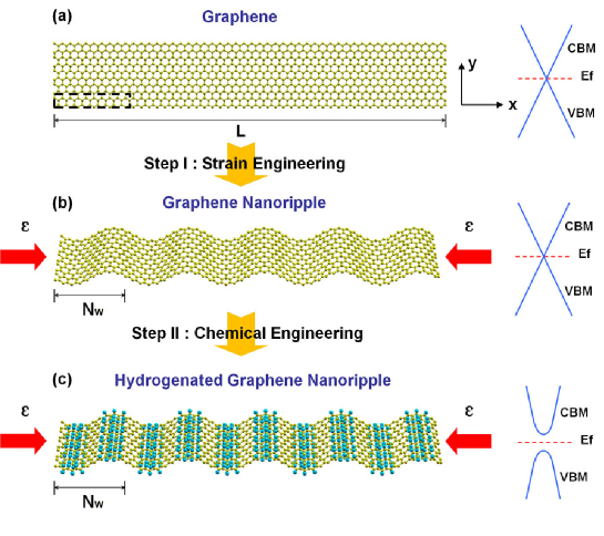
To implement the above mechanisms, the basic idea of our combinatorial approach of strain engineering and directed surface self-assembly is illustrated in Fig. 1. Starting with a pristine graphene sheet of length [Fig. 1(a)], in the first step of ”strain engineering”, a compressive strain () is applied along to form a 1D pattern of graphene nanoripple with period [Fig. 1(b)] [ is the number of dimer and zigzag lines denoting the width of armchair and zigzag nanoripples, respectively (see Fig. 3(a) and 3(d))]. At this step, the nanoripple remains a semimetal. In the second step of ”chemical engineering”, H atoms are introduced to adsorb onto the ripple pattern at designated locations [Fig. 1(c)] to form the HGNRs. Now, band gap opens. The nanoripple formation in the first step has two key functions. First, its period defines the period of the HGNR, i.e. the width of the hydrogenated nanostripes created in the second step, and hence the eventual size of band gap. Second, its morphology serves as a template to direct H atoms to be adsorbed at specific locations with the largest local curvature, so as to form highly ordered H patterns. The directed H adsorption in the second step fulfills the role to open a predefined band gap.
There are several noteworthy advantages of the above approach. The band gap as engineered is tunable with a high level of control. It is well-known that the band gap scales inversely with graphene nanoribbon widths 5 ; 6 ; 7 ; 13 . Here, the width of HGNR is uniquely defined by the period of the nanoripple without H adsorption, which can be tuned precisely by the magnitude of the compressive strain applied and the length of graphene used. Because the H atoms are directed by the nanoripple template to the designated locations of the largest curvature, instead of random adsorption sites, they form a highly regular pattern, which translates the HGNR into an ordered array of graphene nanostripes with the highly uniform width, orientation and smooth edges, so that they all open a predefined uniform band gap. Furthermore, the approach makes a repeatable process, as a cycle of the directed H adsorption and desorption leads naturally to a cycle of metal-semiconductor-metal transition opening the same band gap in the HGNR. In the following, we discuss the processing paramters of the HGNRs and their resulting electronic properties.
We first analyze the strain induced nanoripple pattern formation in graphene, based on a continuum mechanics model 18 ; zhang . Consider a uniaxial compressive strain applied along the x-direction [Fig. 1(b)] of a graphene sheet of length . Above a critical strain value, the flat graphene becomes unstable and undulates into a 1D sinusoidal ripple pattern with period . The total energy of the ripple can be calculated as
where and are the bending and Young’s modulus of graphene, respectively, is the displacement along the z direction, and is the thickness of graphene. Under the boundary condition , , where is the number of ripple period formed and is a constant. Applying the variational principle, the critical strain for generating the ripple pattern can be obtained as
| (2) |
where is the Poisson’s ratio.
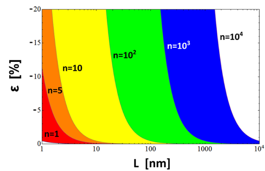
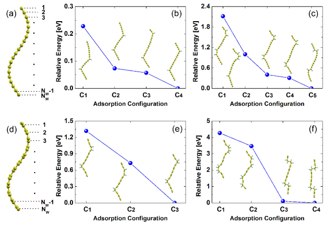
Figure 2 shows the calculated phase diagram showing the number of ripple period () as a function of strain () and graphene length (), using 19 and 20 . For the given (), increases with the increasing (). Thus, the period of ripple pattern () can be tuned by the magnitude of the compressive strain and the length of graphene.
Next, we analyze a ”directed” H self-assembly on the ripple pattern. The ripple morphology provides a curvature template to direct the H adsorption to the designated locations. To illustrate this effect, we compare the total energies of different hydrogen adsorption configurations using the first-principles method. The calculations are performed using the VASP package 21 , which implements the local (spin) density approximation 22 of the density functional theory. The electron-ion interaction is described by the projected augmented wave method 23 with an energy cutoff of and a k-point mesh of () based on the convergence tests. The atom positions are optimized with the atomic force converged to less than .
There are two typical orientations in graphene, i.e. the zigzag and armchair direction 5 ; 6 , along which we apply the compressive strain to form the corresponding armchair and zigzag nanoripple, as shown in Figs. 3(a) and (d), respectively. For the armchair nanoripple, we choose and as an example to demonstrate the directed H adsorption. First, we adsorb two rows of H atoms within one period of the nanoripple to form the armchair HGNR. Comparing the relative adsorption energies (setting the energy per unit cell of the most stable adsorption configuration as the zero energy of reference) [Fig.3(b)], we can see clearly that the H atoms prefer to adsorb onto the carbon atoms with the largest curvature. The H rows divide one ripple period into two equivalent nanostripes of the same width. Next, we absorb another two rows of H atoms, and the stable H adsorption configuration is shown in Fig. 3(c). The additional H rows are attracted to the existing rows, forming two rows of H at the largest curvature locations. Similar directed H adsorption are also observed in the zigzag HGNR with and , as shown in Figs. 3(e) and (f) for two rows and four rows of H atoms within one period of zigzag nanoripple, respectively.
The preferred H adsorption onto the C atoms with the largest curvature is consistent with the previous theoretical 24 and experimental 25 results. This is because instead of the electronic configuration in a planar symmetry, the curved C atom has a configuration, which is closer to the final configuration upon H adsorption 26 . Thus, it costs less energy for H to adsorb onto a curved C atom than onto a planar C atom. Based on the same principle, after H is adsorbed on a C atom, it makes its neighboring C atoms more like, so that the additional H atoms will prefer to adsorb onto these neighboring C atoms, but on the opposite side of graphene.
Formation of graphene nanoripple without H doesn’t open band gap; one role of ripple structure is to provide a template to direct the H adsorption that will open band gap. Also, the period of the nanoripple patterns defines the period of the HGNR, i.e. the width of nanostripes formed upon H adsorption, and hence the final band gap. Next, we present the band gaps of the HGNRs as a function of nanoripple period and strain.
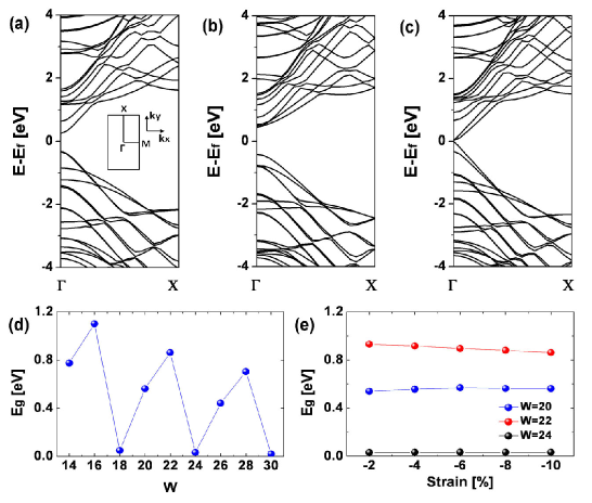
In the direction perpendicular to the H row ( direction), the band structures for armchair and zigzag HGNRs are almost flat, so in the following, we only show the band structures along the H row direction ( direction). The band structures of armchair HGNR adsorbed with two rows of H atoms are shown in Fig. 4, similar to those of armchair graphene nanoribbons 5 ; 6 . Figures 4(a)-(c) are the respective band structures for , and with , in which band gaps can be clearly seen. Without the H, no band gap appears in the armchair nanoripples even when the strain goes up to . The physical origin of the band gap is due to quantum confinement, i.e. the adsorbed H rows remove local bands confining electrons between them. For the fixed strain, the band gap is not a monotonous function of the ripple width, and can be divided into three groups (Fig. 4(d)). They follow the relation, , which is same as that for the armchair graphene nanoribbons 6 . Here is the effective nanostripe width and is a positive integer. For the fixed ripple width, the three band gap groups show little dependence on the strain [Fig. 4(e)]. Without ripple formation, the band gaps of flat armchair nanoribbons have been shown to depend on in-plane uniaxial strain 27 , because strain changes bond length and hence the interatomic electron hopping energies. With the ripple formation, however, the in-plane strain is largely relaxed by the bending (i.e. change of bond angles) so that the bond length changes very little. This is the reason we see a very weak strain dependence of band gap in Fig. 4(e). Note that under compressive strain, the ripple structure is usually favored over the planar graphene, because for normal graphene size (), the critical strain for ripple formation is extremely small (), as shown in Fig. 2.
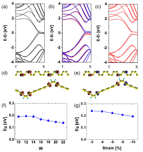
The band structures of zigzag HGNRs adsorbed with two rows of H atoms are shown in Fig. 5, similar to those of zigzag graphene nanoribbons 5 ; 6 . Figures 5(a)-(c) show the band structures of the nonmagnetic (NM), ferromagnetic (FM) and antiferromagnetic (AFM) states with and , respectively. Same as zigzag nanoribbons, the zigzag HGNR in Fig. 5 has an AFM ground state, with the NM and FM states being and higher in energy than the AFM state. The NM state is a metal, with four subbands crossing the Fermi level [Fig. 5(a)]. This is different from the zigzag nanoribbon, which has only two subbands crossing the Fermi level 6 . Because the H atoms divide one ripple period into two nanostripes of the same width, their interaction splits the two subbands into four. The FM state is a metal, while the AFM state is a semiconductor for both spins. The spatial distribution of spin charge densities are shown in Figs. 5(d) and (e) for the FM and AFM states, respectively. For the fixed strain, the band gap of the AFM zigzag HGNR [Fig. 5(f)], opened by symmetry breaking mechanism, shows a much weaker dependence on the ripple width compared to the band gaps of armchair HGNR [Fig. 4(d)], opened by quantum confinement mechanism. For the fixed ripple width, the band gap of the AFM zigzag HGNR [Fig. 5(g)] shows a rather weak dependence on the strain, similar to the case of armchair HGNR [Fig. 4(e)].
In conclusion, we demonstrate theoretically a strain engineered self-assembly process to fabricate a new class of semiconducting graphene based nanostructures, the HGNRs, which share some common band-gap features of graphene nanoribbons. It is a combinatorial two-step process of straining graphene sheet into nanoripples followed by the curvature-directed H adsorption, which offers a high level of band-gap control by tuning the magnitude of strain, the dimension of graphene sheet and the amount of H adsorption. We note that graphene nanoripples have already been fabricated by straining suspended graphene sheet experimentally 28 . The prospect of further dosing the nanoripples with H to form the semiconducting HGNRs is very appealing. We expect that the combination of strain engineered nanoripple formation and the curvature-directed surface self-assembly can be generally applied beyond graphene to other nanomembranes.
This work was supported by DOE, CMSN and BES programs. We thank Center for High Performance Computing at the University of Utah for providing the computing resources.
References
- (1) K. S. Novoselov et al., Nature (London) 438, 197 (2005).
- (2) K. Nakada et al., Phys. Rev. B 54, 17954 (1996).
- (3) Y. W. Son et al., Phys. Rev. Lett. 97, 216803 (2006).
- (4) Q. Yan et al., Nano Lett. 7, 1469 (2007).
- (5) M. Y. Han et al., Phys. Rev. Lett. 98, 206805 (2007).
- (6) X. Li, et al., Science 319, 1229 (2008).
- (7) D. Yu et al., Nano Res. 1, 56 (2008).
- (8) W. Liu et al., Phys. Rev. B 80, 233405 (2009).
- (9) J. Bai et al., Nature Nanotech. 5, 190 (2010).
- (10) A. K. Singh et al., Nano Lett. 9, 1540 (2009).
- (11) H. Xiang et al., Nano Lett. 9, 4025 (2009).
- (12) R. Balog et al., Nature Mater. 9, 315 (2010).
- (13) D. C. Elias et al., Science 323, 610 (2008).
- (14) J. Q. Lu et al., Phys. Rev. Lett. 90, 156601 (2003).
- (15) G. Giovannetti et al., Phys. Rev. B 76, 073103 (2007).
- (16) S. Y. Zhou et al., Nature Mater. 6, 770 (2007).
- (17) E. Cerda et al., Phys. Rev. Lett. 90, 074302 (2003).
- (18) Y. Zhang et al., Appl. Phys. Lett. 96, 111904 (2010).
- (19) Z. C. Tu et al., Phys. Rev. B 65, 233407 (2001).
- (20) J. Zang et al., Commun. Comput. Phys. 2, 451 (2007).
- (21) G. Kresse et al., Phys. Rev. B 47, 558 (1993).
- (22) J. P. Perdew et al., Phys. Rev. B 23, 5048 (1981).
- (23) P. E. Blochl, Phys. Rev. B 50, 17953 (1994).
- (24) L. A. Chernozatonskii et al., J. Phys. Chem. C 114, 3225 (2010).
- (25) P. Ruffieux et al., Phys. Rev. B 66, 245416 (2002).
- (26) D. Yu et al., Nano Lett. 7, 3046 (2007).
- (27) L. Sun et al., J. Chem. Phys. 129, 074704 (2008).
- (28) W. Bao et al., Nature Nanotech. 4, 562 (2009).