Physics of interface: Strongly Correlated Barrier with chemical modulation sandwiched between two metallic planes.
Abstract
Barrier planes described by the Ionic Hubbard model and sandwiched between metallic planes on both sides are studied using unrestricted Hartree Fock. For zero onsite correlation, the presence of the metallic interface generates an additional gap in the energy spectrum away from half filling, if the chemically modulated potential in the barrier planes exceed a critical value. There is reentrant behaviour and an insulator-metal-insulator transition as we tune onsite correlation for fixed site potential. The metal is thus able to penetrate the barrier planes due to proximity effect, in a system that is otherwise an insulator throughout.
pacs:
73.20.-r, 71.27.+a, 71.30.+h, 71.10.Fd, 73.21.b, 73.40.cI Introduction
The emergence of unexpected new properties has made the physics of interface an active research area for some time nowOhtomo ; Millis1 ; Millis2 ; Thiel ; Kenji ; Dagotto1 ; Rosch ; Krish . The interface of a band insulator and Mott insulator was shown to have metallic propertiesOhtomo , which becomes superconducting on lowering the temperatureThiel ; Kenji . Theoretically the subject has been studied using different methods like restricted Hartree FockMillis1 , two site DMFTMillis2 , single site DMFT Rosch ; Krish and Lancsoz Dagotto1 .
In this letter we have studied a metal-quasi 2D barrier-metal heterostructure. The barrier planes are described by the Ionic Hubbard Model, which describes a band insulator with onsite correlation. Thus the barrier planes describe a band insulator in the absence of correlation , and a Mott insulator in the absence of chemical modulation for , where depends on the dimensionality of the system. The ionic Hubbard model has been widely studied by various groups using various techniques like single site DMFTArti ; Craco , quantum monte carloScalettar and cluster DMFT Dagotto2 in 2D, DMRG in 1DBaeriswyl and two site DMFT in quasi 2D Byczuk . At half filling a single site DMFT solution which assumes a paramagnetic solution yields a metallic phase which separates the Mott insulator and band insulator phasesArti ; Craco . A solution which incorporates long range anti-ferromagnetic ordering in quasi 2D, using two site DMFT, however shows that the system is insulating for all interaction strengths.
The Mott insulator-band insulator heterostructure has been studied using restricted Hartree Fock Millis1 , inhomogeneous two site DMFT Millis2 and in quasi one dimensional lattices using Lancsoz method Dagotto1 . The metal-Mott insulator-metal heterostructure has been studied Rosch ; Krish ; Gupta2 while the role of disorder on the Mott planes has also been investigated by us Gupta3 .
Spatial variations in the planes and along the z direction play a crucial role in determining the correct ground state of a highly inhomogeneous systems like heterostructures. The in plane variation is totally ignored in a one site inhomogeneous DMFT(IDMFT)Georges ; Metzner ; Potthoff ; freericks_idmft approach. The two site IDMFT method though capable of capturing planar long range order like planar antiferromagnetism, is insufficient to capture the regime where the two orders start to cancel each other leading to short range ordering. With this in mind we have adopted the method of unrestricted Hartree Fock. The Hartree Fock method has been used successfully to describe the ground state of the ionic Hubbard model even in 1D and was shown to be in excellent agreement with real space RG calculationSanjay .
I.1 Model and Method
The Hamiltonian for the system is
| (1) | |||||
Here the label indexes the planes, and the label indexes sites of the two-dimensional square lattice in each plane. The operator () creates (destroys) an electron of spin at site on the plane . We set the in-plane hopping to be nearest neighbor only, and equal to , the hopping between planes, so that the lattice structure is that of a simple cubic lattice. We take for the sites and for the sites. We also take for the barrier planes, and zero for the metallic planes. The chemical potential is calculated by taking the average of the N/2 th and the N/2 + 1 th energy level. The plane index correspond to the metallic layers. All the other values in between correspond to the barrier planes. For the quasi 2D geometry taken by us total number of sites , where is the total number of layers and is the number of sites in the planes.
|
|
|
|
|
|
I.2 Calculated quantities
We have calculated the energy spectrum, charge and spin profile, and the optical conductivity. The charge at site is given by: = + . The spin at a particular site is given by = . The optical conductivity is calculated using the Kubo formula. In this paper, is calculated in units of . For details of the calculation procedure see our previous workSanjeevEPL ; Gupta1 . We have performed finite size scaling of each of our transport results. The value of is calculated for multiples of a small , where is twice the lowest that we can access for a particular system size.
|
|
|
|
I.3 Analysis of our results
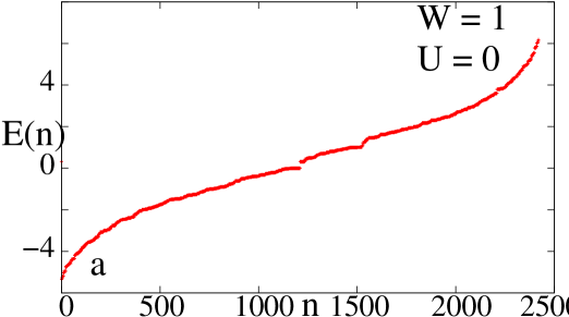
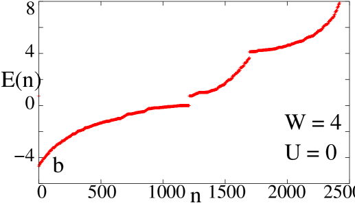
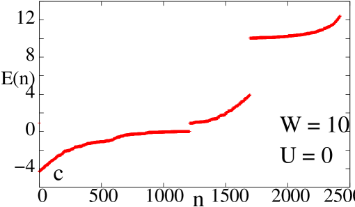
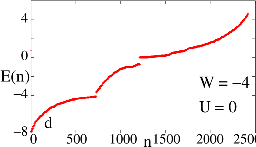
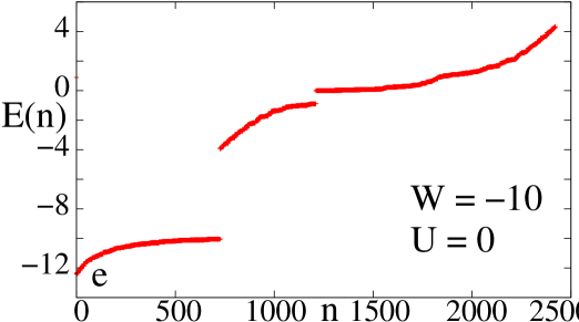
Fig 1a,b,c,d,e and f shows that different types of sites emerge as we systematically tune . positive/negative corresponds to repulsive/attractive potential/wells in the barrier planes. In the absence of any non-zero leads to a charge density wave(CDW) profile, with a symmetry in the gap about the origin. Increasing beyond a certain threshold value, an additional gap opens up away from half filling. The value of the gap which would have been identical to in the absence of the metallic planes gets reduced in the presence of the metallic planes. This gap is due to the fact that the barrier planes induce a density modulation even in the metallic planes due to proximity effect. Thus the entire system has a rather inhomogeneous alternate density modulation. As we increase further at around , a second gap opens up. For general , the filling at which the second gap opens up is given by 0.5 + sign(W)*(1/m). Above this value , the lowly occupied sites in the barrier planes(B sites) become very different from the lowly occupied sites in the metallic planes and a new band emerges. For negative the second gap opens at = -4. The states below this new band gap now correspond to the B sites from the barrier planes and the states above the gap correspond to lowly occupied sites from the metallic planes. Due to -ve value of the system can now lower energy by doubly occupying the sites. The gap at half filling saturates to a fixed value as we keep on increasing . This is because the higher energy B sites(both in the barrier and those induced in the metallic planes) are now more or less avoided by the electrons.
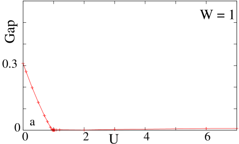
In Fig 2a, we show the modulation of the gap at half filling for = 1 as we increase . The band gap is suppressed by down to zero, after which there is a large gapless region. The low region corresponds to a CDW phase, where has started to compete with the chemical modulation with the latter being dominant. The large gapless region corresponds to a highly inhomogeneous phase, with no spin order till and with gradually diminishing but non zero charge order. Above , spin order starts to pick up gradually, though there is still a remnant weak charge order also.
|
|
|
|
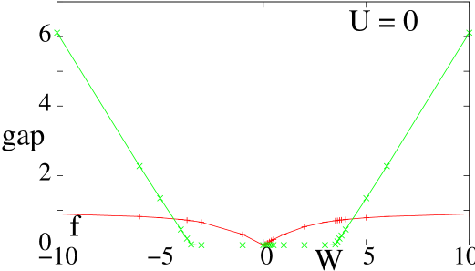
Fig 2b shows the variation of the two gaps in the energy spectrum for = 7, for both spins with variation in . In the absence of , the opening up of two gaps in the energy spectrum was first shown by us in a previous work Gupta2 . For positive values of , till , both the gaps for both spins fall monotonically with increasing . There is small spin asymmetry which is a signature of spontaneous symmetry breaking of the up and down spin sectors for such a system. This behaviour has already been observed and reported by Cabib and Callen C&C for an extended Hubbard () model.
While for positive the sites are avoided by the electrons, The repulsion of the electrons to the metallic planes takes place uniformly for both up and down spins because there is very small charge modulation in the metallic planes and since there is on all the barrier plane sites, they would all like to push electrons away to the metallic planes, without paying the cost of .
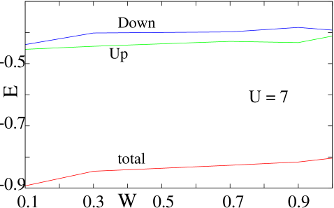
Fig 2c shows the plots of energy for both spin species and the total energy as we modulate for . The total energy increases monotonically with increasing . The energy for the two spin species are different for the entire parameter range where there is both charge and spin order. This is a signature of the spin asymmetry reported earlierC&C .
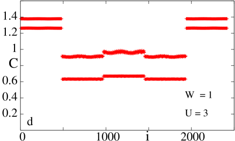
2d shows the plots of the charge profile for . The overall symmetry of the profiles about the central plane and the explicit z dependence are seen. In this regime where has just killed the gap due to anti ferromagnetic long range order due to , there is already a strong plane dependent CDW ordering.
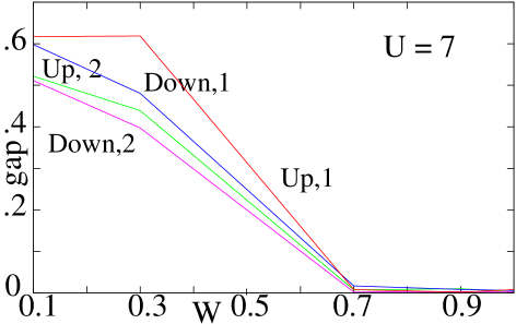
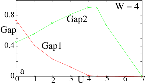
In Fig 3a we have shown the variation of the two gaps that opens up for = 4 with increase in . We see that the two gaps behave in very contrasting manner with increasing . While the gap at half filling falls off monotonically to zero, which basically implies that the charge ordering induced in the metallic planes by is killed by . However the second gap for positive shows a non monotonic variation with . It first increases with increasing and then after a certain value of starts to decrease. This is because for low values of , the electrons in the A sites of the interface layer start to deplete by moving to the metallic planes. The occupancy of the B sites however is relatively unaffected in this regime. Thus the second gap which senses the difference between the topmost level of the second band and the lowest level in the topmost band increases. However beyond a certain threshold, the B sites in the barrier planes start to get occupied and then the gap starts falling.
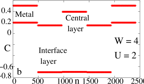
Figs 3b,c,d show the charge profile for = 2,3,6 respectively for = 4. While for = 2 and 3, the gap at half filling decreases but is still non zero, for = 6 the gap at half filling has already become zero. This we can see clearly from the figures, where for = 2 and 3, there is inhomogeneous CDW ordering in all the planes. For = 6 however the CDW ordering is destroyed in the metallic planes.
|
|
|
|
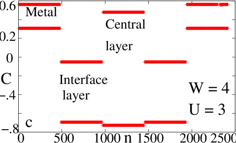
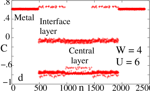
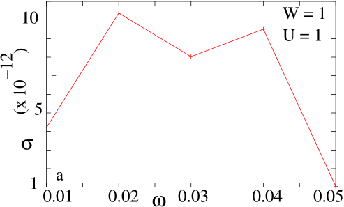
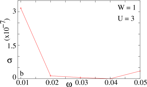
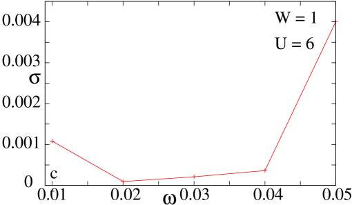
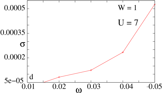
Figs 4a,b,c,d show the plots of optical conductivity versus for = 1,3,6 and 7 respectively for = 1. As we tune keeping fixed, the system exhibits reentrant behaviour in the form of an insulator-metal-insulator transition. As the gap at half filling gets killed initially around = 1, a residual slightly weakened CDW ordering persists in the system all the way upto = 6. The A sites in the barrier start to deplete and the B sites are relatively unaffected for low . As we increase further, the system becomes a metal as seen in = 3 and 6. The metal at = 3 is a much weaker one compared to the one at = 6, as the charge ordering is fully destroyed for = 6. The weak metallic behaviour for = 3 inspite of the presence of charge ordering in the system is a consequence of weak tunneling of electrons between the sites. For = 7, a small inhomogeneous spin order develops in the system, which drives the system to an insulating phase.
II Conclusion
A barrier described by the ionic Hubbard model sandwiched between two metallic planes has been studied using unrestricted Hartree Fock. Increasing the strength of the site potential modulation, beyond a critical strength opens a new gap away from half filling at a value that depends on the sign of the modulation. Below onset of correlation reduces the gap to zero gradually. Above while the gap at half filling follows the same pattern, the new gap shows non monotonic behaviour with increasing . The system shows reentrant insulator-metal-insulator transition with increasing for fixed = 1. Spin asymmetric behaviour is noticed when both charge and spin order is present in the system.
References
- (1) A. Ohtomo et al., Nature (London), 419, 378 (2002), Nature (London), 427, 423 (2004).
- (2) S. Okamoto and A. J. Millis, Nature (London),428, 630 (2004); Phys. Rev. B, 70, 241104(R) (2004);
- (3) S. Okamoto and A. J. MillisPhys. Rev. B,72, 235108 (2005).
- (4) S. Thiel, G. Hammerl, A. Schmehl, C. W. Schneider, and J. Mannhart, Science, 313, 1942 (2006)..
- (5) Kenji Yonemitsu, Nobuya Maeshima and Tatsuo Hasegawa, Phys. Rev. B.,76, 235118, (2007)
- (6) S. S. Kancharla, E. Dagotto, Phys. Rev. B,74, 195427 (2006).
- (7) R. W. Helmes, T. A. Costi, and A. Rosch, Phys. Rev. Lett. 101, 066802 (2008).
- (8) H. Zenia, J. K. Freericks, H. R. Krishnamurthy, Th. Pruschke , Phys. Rev. Lett., 103, 116402, (2009).
- (9) Arti Garg, H. R. Krishnamurthy, M. Randeria, Phys. Rev. Lett., B 97, 046403 (2006);
- (10) L. Craco, P. Lombardo, R. Hayn, G. I. Japaridze, and E. Müller-Hartmann, Phys. Rev. B,78, 075121 (2008)
- (11) K. Bouadim, N. Paris, F. Hébert, G. G. Batrouni, and R. T. Scalettar, Phys. Rev. B 76, 085112 (2007)
- (12) L. Tincani, R. M. Noack, and D. Baeriswyl,Phys. Rev. B 79, 165109 (2009)
- (13) K. Byczuk, M Sekania, W Hofstetter and Arno P. Kampf, Phys. Rev., B 79, 121103 (2009);
- (14) S. S. Kancharla and E. Dagotto, Phys. Rev. Lett., 98, 016402 (2007)
- (15) Sanjay Gupta and Tribikram GuptaarXiv, 1003.4642
- (16) Sanjay Gupta and Tribikram GuptaarXiv, 1009.5601
- (17) A. Georges, G. Kotliar, W. Krauth, and M. J. Rozenberg, Reviews of Modern Physics, 68, 13 (1996).
- (18) W. Metzner and D. Vollhardt, Phys. Rev. Lett., 62, 324 (1989).
- (19) M. Potthoff and W. Nolting, Phys. Rev., B 59, 2549 (1999); S. Schwieger, M. Potthoff, and W. Nolting, ibid. 67, 165408 (2003).
- (20) J. K. Freericks, Phys. Rev. B 70, 195342 (2004).
- (21) Sanjay Gupta, Shreekantha Sil and Bibhas Bhattacharyya, Phys. Rev. B,63 125113 (2001).
- (22) Tribikram Gupta and Sanjay Gupta, Euro Physics Letters 88, 17006 (2009)
- (23) Sanjeev Kumar and Pinaki Majumdar, Europhys. Lett 65, 75 (2004)
- (24) Dario Cabib and Earl Callen, it Phys. Rev. B, 12 5249 (1975)