Reverse Schottky-Asymmetry Spin Current Detectors
Abstract
By reversing the Schottky barrier-height asymmetry in hot-electron semiconductor-metal-semiconductor ballistic spin filtering spin detectors, we have achieved: 1. Demonstration of 50% spin polarization in silicon, resulting from elimination of the ferromagnet/silicon interface on the transport channel detector contact, and 2. Evidence of spin transport at temperatures as high as 260K, enabled by an increase of detector Schottky barrier height.
Measurement of spin transport in semiconductors has been achieved by detecting either spin-accumulation (density)Lou et al. (2007); Salis et al. (2009); Sasaki et al. (2010); van ’t Erve et al. (2007), or spin current. The latter configuration has been achieved in silicon (Si) devices by exploiting the mean-free-path (mfp) asymmetry between spin-up and spin-down hot electrons in ferromagnetic (FM) thin films: electrons are ejected from the conduction band of the semiconductor forming the transport channel, and the ballistic component of this current is collected on the other side of the FM by a Schottky barrier.Appelbaum et al. (2007)
The design of these detectors has incorporated the fact that to maximize the hot electron collection efficiency (namely, the “transfer ratio” of the ballistic current to the current flowing through the channel ), the collector Schottky barrier should be lower than the average hot electron energy defined by the Schottky barrier on the transport side. This design rule has resulted in the “normal” detector shown in Fig. 1(a), where hot electrons ejected from Si on the left first pass through the NiFe ferromagnet and then over the (lower) Cu/n-Si Schottky barrier. Although this design has enabled many fundamental measurements (e.g. spin transport through the full wafer thicknessHuang et al. (2007a), across 2 mm in quasilateral devicesHuang et al. (2008), in doped SiJang et al. (2008), and long-distance lateral spin transport close to the buried Si/SiO2 interfaceJang and Appelbaum (2009)), the FM/Si interface present reduces the observed spin polarization. This is due to the presumed formation of a magnetically-dead silicideHuang et al. (2007b), and the low Cu/n-Si Schottky barrier limits operation to 200K when thermionic leakage and its concomitant noise sufficiently dilutes the spin transport signal.
In this Letter, we describe an alternative spin detector design where the FM is not in contact with the Si spin transport channel and the Schottky barrier height asymmetry is reversed. This design circumvents the problems discussed above and results in observations of both higher spin polarization and higher temperature operation.

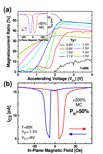
Our “reversed” detector design is shown in Fig. 1 (b). Because the NiFe/n-Si Schottky barrier is higher than Cu/n-Si, electrons with low energy close to the conduction band edge on the transport side have no possibility to couple with conduction band states in the n-Si collector on the other side, and the detector hot electron collection efficiency transfer ratio is indeed lower. Spin-valve transistorsMonsma et al. (1995, 1998); Jansen (2003) have been demonstrated in this reversed asymmetry as well.Kumar et al. (2000); Jansen et al. (2001) However, the first benefit of this detector design is that by removing the possibility of silicide formation in the region before the electron spin is analyzed in the NiFe bulk, higher spin polarizations can be observed. This is because non-magnetic silicides of bulk elemental ferromagnet ions have large, randomly oriented magnetic moments that cause massive spin relaxation.Veuillen et al. (1987); Tsay and Yao (1999) Removal of a FM/Si interface at the injector side was previously shown to increase spin polarization from 1%Appelbaum et al. (2007) to 37%.Huang et al. (2007c) Using a magnetic-tunnel-junction (MTJ)-type spin injectorHuang et al. (2007b) and a 3-thick 1-10 n-type Si transport channel in a vertical device geometryJang et al. (2008), we can observe a magnetocurrent change (, where the superscripts and refer to parallel and antiparallel magnetic configuration, respectively) of greater than 50% (shown with in-plane magnetic field measurements in Fig. 2(a)). This is significantly higher than the 6% previously reported in devices using identical injector and the “normal” detector design.Jang et al. (2008) Because this injector suffers from greatly reduced injected polarization at high tunnel-injector bias (), we also present measurements from devices with a ballistic-spin-filtering spin injector (similar to Ref. [Huang et al., 2007c] where 37% spin polarization was reported). In this case (shown in Fig. 2(b)), over 200% magnetocurrent (corresponding to 50% spin polarization in the Si transport channel) can be seen.
Because the low-energy portion of the electron distribution (determined by the product of Boltzmann occupation distribution and the conduction band density of states) does not play a role in the collected current , this detector has a lower transfer ratio than the normal detector design. However, as the thermal energy increases, a greater fraction of electrons occupy the high-energy tail of the distribution and the transfer ratio should increase. This behavior is clearly shown at low accelerating voltages in Fig. 3(a), where the data (right axis) is from MTJ-type injector devices. Despite a consistent trend with temperature in the magnetocurrent (left axis), this transfer ratio trend reverses at accelerating voltages above 2.5V, where large electric fields V/cm can accelerate electrons to kinetic energy on the order of the Schottky barrier asymmetry within a mfp . Under these circumstances, all electrons can potentially contribute to the spin signal (i.e. energy conservation is no longer an obstacle to transport) and inelastic scattering in the metal film bulk (which increases with temperature) largely determines the temperature dependence of the transfer ratio. The inset to Fig. 3(a) illustrates this high-field effect.
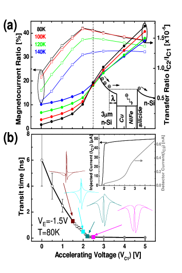
This explanation based on internal electric-field is confirmed by measurements where the magnetic field is perpendicular to the plane, and Hanle spin precession and dephasing is detected. In Fig. 3(b), transit times extracted from the width of the quasi-Lorentzian Hanle data measured in the range 850Oe show that at slightly lower accelerating voltages than the crossover value in the transfer ratio temperature trend (see vertical dotted line in Fig. 3(a)), the transit time collapses. This corresponds to a removal of the confining potential in the conduction band of the transport channel caused by depletion regions on both the injector and detector sides. In a fully depleted model, the donor density consistent with this catastrophe at 2V is given by 31014 cm-3. This is somewhat less than in similar low-doped Si transport channel devices previously reportedJang et al. (2008), which can easily be due to doping variation between wafers.
For further confirmation of the low-field ( V) device behavior, we model the temperature dependence of the detector transfer ratio by calculating the fraction of electrons in the transport channel which have more energy than the Schottky asymmetry via a semiclassical approximation (see Fig. 1(b) for illustration):
| (1) |
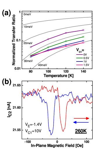
where all other factors (effective mass, etc.) cancel, and we have not taken into account the role of inelastic scattering in the metal thin films. Note that this model also does not incorporate the high-field behavior schematically illustrated in the inset to Fig. 3(a). Therefore, we compare the model prediction from evaluation of Eq. (1) in Fig. 4(a) for several values of to empirical transfer ratios only for 2.5 V. Furthermore, we normalize these empirical values by those from a similar device with “normal” detector (not shown) to remove the temperature dependence of the inelastic scattering in the metal thin films and reveal only the effect of Schottky asymmetry. As can be seen in Fig. 4(a), our results are consistent with a Schottky asymmetry of 30meV, close to the known difference between Cu and Ni/Fe Schottky barriers on n-Si.Sze (1981)
This modest 30meV increase in collector Schottky barrier actually has substantial impact on the operating temperature of these spin transport devices. Since Schottky leakage current is super-exponentially dependent on temperature, the high-temperature limit to operation is very sensitive to barrier height. With Cu/n-Si detectors, our temperature of operation is limited to 200K before thermionic leakage sufficiently degrades performance. In this alternative “reversed” Schottky asymmetry detector, we can now make spin-valve measurements consistent with spin transport up to 260K, as shown in Fig. 4(b) using the 3m-thick vertical n-Si devices with MTJ-type injectors previously described. Therefore, we expect the spin detector discussed here to have implications for studying true spin transport in semiconductors under conditions approaching room-temperature (300K).
This work was supported by the Office of Naval Research and the National Science Foundation. We acknowledge the support of the Maryland NanoCenter and its FabLab.
References
- Lou et al. (2007) X. Lou, C. Adelmann, S. Crooker, E. Garlid, J. Zhang, S. Reddy, S. Flexner, C. Palmstrøm, and P. A. Crowell, Nature Phys. 3, 197 (2007).
- Salis et al. (2009) G. Salis, A. Fuhrer, and S. F. Alvarado, Phys. Rev. B 80, 115332 (2009).
- Sasaki et al. (2010) T. Sasaki, T. Oikawa, T. Suzuki, M. Shiraishi, Y. Suzuki, and K. Noguchi, Appl. Phys. Lett. 96, 122101 (2010).
- van ’t Erve et al. (2007) O. van ’t Erve, A. Hanbicki, M. Holub, C. Li, C. Awo-Affouda, P. Thompson, and B. Jonker, Appl. Phys. Lett. 91, 212109 (2007).
- Appelbaum et al. (2007) I. Appelbaum, B. Huang, and D. J. Monsma, Nature 447, 295 (2007).
- Huang et al. (2007a) B. Huang, D. J. Monsma, and I. Appelbaum, Phys. Rev. Lett. 99, 177209 (2007a).
- Huang et al. (2008) B. Huang, H.-J. Jang, and I. Appelbaum, Appl. Phys. Lett. 93, 162508 (2008).
- Jang et al. (2008) H.-J. Jang, J. Xu, J. Li, B. Huang, and I. Appelbaum, Phys. Rev. B 78, 165329 (2008).
- Jang and Appelbaum (2009) H.-J. Jang and I. Appelbaum, Phys. Rev. Lett. 103, 117202 (2009).
- Huang et al. (2007b) B. Huang, L. Zhao, D. J. Monsma, and I. Appelbaum, Appl. Phys. Lett. 91, 052501 (2007b).
- Huang et al. (2007c) B. Huang, D. J. Monsma, and I. Appelbaum, Appl. Phys. Lett. 91, 072501 (2007c).
- Huang and Appelbaum (2008) B. Huang and I. Appelbaum, Phys. Rev. B 77, 165331 (2008).
- Monsma et al. (1995) D. Monsma, J. Lodder, T. Popma, and B. Dieny, Phys. Rev. Lett. 74, 5260 (1995).
- Monsma et al. (1998) D. Monsma, R. Vlutters, and J. Lodder, Science 281, 407 (1998).
- Jansen (2003) R. Jansen, J. Phys. D 36, R289 (2003).
- Kumar et al. (2000) P. S. A. Kumar, R. Jansen, O. M. J. van ’t Erve, R. Vlutters, P. de Haan, and J. C. Lodder, J. Magn. Magn. Mat. 214, 1 (2000).
- Jansen et al. (2001) R. Jansen, O. M. J. van ’t Erve, S. D. Kim, R. Vlutters, P. S. A. Kumar, and J. C. Lodder, J. Appl. Phys. 89, 7431 (2001).
- Veuillen et al. (1987) J. Y. Veuillen, J. Derrien, P. A. Badoz, E. Rosencher, and C. Danterroches, Appl. Phys. Lett. 51, 1448 (1987).
- Tsay and Yao (1999) J. S. Tsay and Y. D. Yao, Appl. Phys. Lett. 74, 1311 (1999).
- Sze (1981) S. Sze, Physics of Semiconductor Devices, 2nd edition (Wiley-Interscience, New York, 1981).