Mesoscopic spin Hall effect along a potential step in graphene
Abstract
We consider a straight one-dimensional potential step created across a graphene flake. Charge and spin transport through such a potential step are studied in the presence of both intrinsic and extrinsic (Rashba) spin-orbit coupling (SOC). At normal incidence electrons are completely reflected when the Rashba interaction (with strength ) is dominant whereas they are perfectly transmitted if the two types of SOC are exactly balanced. At normal incidence, the transmission probability of the step is thus controlled continuously from 0 to 1 by tuning the ratio of the two types of SOC. Besides the transport of charge in the direction normal to the barrier, we show the existence of a spin transport along the barrier. The magnitude of the spin Hall current is determined by a subtle interplay between the height of the potential step and the position of Fermi energy. It is demonstrated that contributions from inter-band matrix elements and evanescent modes are dominant in spin transport. Moreover, in the case of vanishing extrinsic SOC (), each channel carries a conserved spin current, in contrast to the general case of a finite , in which only integrated spin current is a conserved quantity. Finally, we provide a quasi-classical picture of the charge and spin transport by imaging flow lines over the entire sample and Veselago lensing (negative refraction) in the case of a junction.
pacs:
1I Introduction
Within the last decade the role of SOC in pure crystals has been fundamentaly reconsidered thereby providing a host of novel effects Murakami et al. (2003); Sinova et al. (2004); Kato et al. (2004); Wunderlich et al. (2005) and phases Kane and Mele (2005a, b); Bernevig et al. (2006); König et al. (2008); Qi and Zhang (2010a); Moore (2010); Hasan and Kane (2010); Qi and Zhang (2010b) with potential applications in spintronics.
First it was predicted that SOC may generate a transverse spin current in response to an applied electric field both in hole and electron doped semiconductors Murakami et al. (2003); Sinova et al. (2004). This so-called intrinsic spin Hall effect was promptly reported by the detection of the related spin accumulation at the boundaries of GaAs samples Kato et al. (2004); Wunderlich et al. (2005).
More recently SOC was shown to lead to a topological phase of electronic matter when combined with a particular band inversion property Kane and Mele (2005a, b); Bernevig et al. (2006); König et al. (2008, 2007); Roth et al. (2009); Qi and Zhang (2010a); Moore (2010); Hasan and Kane (2010); Qi and Zhang (2010b). In two-dimensional systems this so-called Quantum Spin Hall (QSH) state is characterized by metallic edge states surrounding an insulating bulk. Those edge states show up in the absence of magnetic field and realize a time-reversal invariant version of the chiral edge states of the Integer Quantum Hall states. Initially the QSH state was introduced in the Kane-Mele model of graphene which describes non-interacting electrons on honeycomb lattice with both intrinsic and extrinsic SOC Kane and Mele (2005a, b). In the Kane-Mele model, intrinsic SOC conserves the -component the real spin () and generates a topological mass term. In contrast the extrinsic Rashba-type SOC breaks conservation by mixing (spin ) and (spin ) spin components. When the intrinsic SOC dominates the Rashba one, the bulk excitations are gapped and a pair of gapless states counter-propagate along an edge of the sample. Nevertheless the weakness of the SOC induced gap Min et al. (2006); Huertas-Hernando et al. (2006); Yao et al. (2007) makes the realization of the QSH state extremely difficult in graphene. In contrast similar QSH edge states have been predicted Bernevig et al. (2006) and soon after reported in transport experiments, performed in HgTe/CdTe quantum wells König et al. (2008, 2007); Roth et al. (2009).
In a recent paper Yamakage et al. (2009), we have shown that charge transport through a potential step allows to investigate the relative strength of intrinsic and extrinsic SOCs. In the absence of SOC, the transmission of electrostatic potential steps have been extensively studied in graphene both experimentaly Huard et al. (2007); Williams et al. (2007); Özyilmaz et al. (2007); Oostinga et al. (2008); Gorbachev et al. (2008); Liu et al. (2008) and theoretically Katsnelson et al. (2006); Cheianov and Falko (2006); Cayssol et al. (2009) with the purpose of providing a condensed-matter implementation of the relativistic Klein tunneling. In practise such potential steps can be induced either by a distant gate Huard et al. (2007); Williams et al. (2007); Özyilmaz et al. (2007); Oostinga et al. (2008); Gorbachev et al. (2008); Liu et al. (2008) or by metallic contacts Huard et al. (2008); Stander et al. (2009).
In this paper we detail supplementary aspects of the charge transport properties outlined in Yamakage et al. (2009). In addition we emphasize here the spin transport near an electrostatic potential step. As a main result, an interfacial spin Hall effect is predicted, which we call hereafter mesoscopic spin Hall effect (MSHE). In the MSHE the spin current flows in the direction transverse to the applied electric field, and is mainly localized at the vicinity of the step. Owing to this nonuniform spin current distribution, the MSHE differs from the spin Hall effect in homogeneous doped semiconductors Murakami et al. (2003); Sinova et al. (2004); Kato et al. (2004); Wunderlich et al. (2005) and in graphene Dyrdałet al. (2009).
The paper is organized as follows. In Sec. II, the charge and spin current operators for the Kane-Mele model are derived in presence of intrinsic and Rashba SO coupling. It is shown in section III that quantum averages of these operators consist of direct and cross (interference) terms when computed within a generic scattering state. We discuss charge transport in Section IV. As a main prediction of this paper, the spin transport along the interface (transverse to the applied electric field) is described thoroughly in the section V while possible experimental detection is also discussed therein. Finally, we provide a quasi-classical picture of the charge and spin transport by imaging flow lines on the entire sample and Veselago lensing (or negative refraction) at the junction.
II Formalism: charge and spin currents
We consider a graphene monolayer in the presence of both intrinsic and extrinsic SOC . The corresponding charge and spin current operators are constructed in the framework of the Kane-Mele model of graphene Kane and Mele (2005a, b). The quantum averages of the charge and spin currents are derived both for propagative and for evanescent quasiparticles.
II.1 Kane-Mele model
The low-energy Kane-Mele model Kane and Mele (2005a, b) is defined by the Hamiltonian with
| (1) |
Here are the Pauli matrices associated with the lattice isospin ( and sites of the honeycomb lattice), the valley-isospin ( and points of the reciprocal space), and the real electronic spin, respectively.
The kinetic Hamiltonian describes graphene in the absence of any spin-orbit interaction. The intrinsic spin-orbit effect (with coupling constant ) is described by which preserves all the symmetries of the problem and further conserves the component of the electronic spin. In contrast the Rashba contribution (with coupling constant ) explicitely breaks the conservation of .
The full Kane-Mele Hamiltonian acts on -spinors. Nevertheless in this paper we will only consider intravalley scattering caused by electrostatic potential steps. Hence we shall focus on the -valley in the following analysis and simply substitute () in Eq.(1). The resulting Hamiltonian consists of a matrix acting on a spinor of the form , where , stands for real spin.
In the homogeneous case (in the absence of spacially varying potential), the momentum is a good quantum number. The single-valley Hamiltonian is diagonalized by the eigenstates as
| (2) |
where indices specify the band. The dispersion relation of the band reads
| (3) |
and the corresponding wavefunction can be expressed as
| (4) |
with
| (5) |
These wavefunctions are normalized to represent a unit probability within a rectangular graphene flake of length (along the -direction) and width (along the -direction).
In the presence of a potential step or a sample edge, evanescent states appears. Their spectrum and wave functions are given, respectively, by Eqs. (3,4,5) with typically an imaginary . Note also that . Boundedness of the wave function does not allow evanescent modes to exist in an ideally infinite system. They are, nevertheless, ubiquitous in any hetero-junctions (near potential steps) or even at a sample termination. The helical edge states, on the other hand, occur only at the boundary between two topologically distinguishable phases each characterized by opposing indices. In the case of topological insulator, index distinguishes trivial (even number of Kramer’s pairs) vs. non-trivial (odd number of Kramer pairs) insulating states.
II.2 Charge and spin current operators
We construct here the charge and spin current operators associated with the single-valley Kane-Mele Hamiltonian . We simply write the continuity equations for the charge and the -component of the electronic spin. The charge and spin density operators ( and respectively) can be written as,
| (6) | ||||
| (7) |
using the four component field operators and . The charge current operator is determined such that it satisfies the continuity equation for charge:
| (8) |
Using the equation of motion
| (9) |
it is readily verified that the operator defined as,
satisfies Eq. (8). This expression can be alternatively obtained from the usual definition of the charge current,
and by noting that the only momentum-dependent part of is , ().
We repeat the same procedure by introducing the spin current operator for -spin component as
| (10) |
However, in the presence of Rashba SO coupling, the second term on the r.h.s. of Eq. (9) does not commute with , leading to a source term in the continuity equation for spin:
| (11) |
The source term describes the spin torque due to Rashba spin orbit interaction. Violation of the continuity equation leads in many cases to the ambiguity in the definition of spin current density, reflecting correctly the fact that spin is not conserved. However, as far as spin transport in our junction problem is concerned, we will see later in Sec. V that the spin current density defined as Eq. (10) yields a conserved spin current when integrated over the incident angle . Such a spin current satisfies the continuity equation globally, i.e. in the sense of
| (12) |
where denotes averaging over the scattering states. The spin current density (10) becomes locally conserved in the absence of Rashba SO coupling: .
II.3 Charge and spin current carried by an eigenstate
We now evaluate the quantum average of the charge and -spin currents in the eigenstate defined by Eq. (4). When both and are real, this state corresponds to a propagating plane wave and carries the charge current density
| (13) |
which is collinear to the momentum . This current consists in equal contributions from the channels and . Moreover these contributions correspond to opposite spin currents leading to a cancellation of spin current for the -spin component. This statement is confirmed by direct calculation of the quantum average of the -spin current
| (14) |
in the bulk eigenstate .
In presence of a potential step or at a sample edge, evanescent states, described by an imaginary , become possible. If we assume a semi-infinite graphene plane extending over the half-plane (), the charge current carried by such an evanescent wave reads
| (15) | ||||
| (16) |
The current is localized near the interface and flows along the axis. Moreover the net charge transport vanishes when the sum over is performed.
Finally the average of the spin current in an evanescent state,
| (17) | ||||
| (18) |
shares the characteristics of the charge current except that spin current will not vanish upon integration (see section V).
III Scattering states for a potential step
We consider a potential step in a graphene monolayer as shown in Fig. 1 and construct the corresponding scattering states. We evaluate the quantum averages of the charge and spin current densities in a given scattering state. Owing to the spin-orbit coupling (i.e. multiband character of the Kane-Mele model), the structure of those averages is more complicated than the average currents in a pure eigenstate . Indeed a single incident electron generates two transmitted electronic waves. Therefore the averaged currents contain direct terms involving only one kind of quasiparticles, and crossed terms describing coherent interferences between the two transmitted waves.
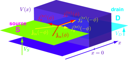
III.1 The junction model
We consider an electrostatic gate creating a potential step which is slowly varying on the scale of the atomic lattice. Moreover we assume an ideally pure system which can be approached in experiments with suspended devices. These conditions ensure that intervalley scattering can be neglected and that the junction is described by the Hamiltonian
| (19) |
where and represent the identity in lattice isospin and real spin space, respectively. Besides, we further assume that the step is sharp on the scale of the Fermi wavelength. In this sense we may represent the potential by an abrupt step defined by
| (20) |
Note that we also assume a straight interface with translational invariance along the direction (no roughness along the interface ).
III.2 Scattering states
Typical scattering state with energy and transverse momentum
| (21) |
can be constructed in terms of the bulk eigenstates Eq. (4). It is assumed here that the incident electron is a pure state. Hence the incident and reflected waves read
where (resp. ) corresponds to the incident (resp. reflected ) wave, and
The -component of the momentum is the positive solution of . There is also an evanescent state defined in the half-plane ,
and localized near the interface . The value of is set by the positive solution of
Within the half-plane , the scattering state consists of two transmitted waves with opposite symmetry and , described by the spinors
where the -components of the momentum are obtained by solving . Note that can be either real or imaginary. When is real, stands for a propagating mode and the sign of is chosen such that the group velocity is positive, i.e. correctly describes an outgoing wave. When is imaginary, is an evanescent mode and the sign of the imaginary part of is fixed by the requirement of wavefunction boundness at .
It is sometimes more convenient to specify by and an incident angle , instead of and the transverse momentum
| (22) |
Finally the four scattering amplitudes , , and are uniquely determined by solving the continuity condition at Yamakage et al. (2009):
| (23) |
for given , and (or ).
III.3 Direct and crossed terms
We have seen that the scattering state takes the form of a superposition of two bulk states with opposite band symmetry . The expectation value of current density in such scattering state
| (24) |
has naturally two types of contributions: direct and crossed terms. The direct terms (proportional to and ) are similar to the ones addressed in the previous section, see Eqs. (13,14,15,16,17,18). In particular such direct terms were shown to carry no net -spin current when associated with a propagative wave (Eq.(14)) whereas evanescent waves carry a finite spin current (Eq.(17)). In contrast the crossed terms always contribute to spin transport regardless of the nature of the two interfering transmitted waves.
In the following we focus on the charge and spin transport associated with these latter crossed terms which mix the transmitted waves and altogether. The crossed charge current is proportional to the expression
| (25) |
where while and were defined in the previous subsection. These crossed terms yield a charge current along the -axis. In contrast to the direct terms, the crossed current has a spacial dependence upon the coordinate (dependence upon is forbidden by translational invariance). The total current is therefore divergenceless.
We now consider the spin current. The crossed terms are proportional to:
| (28) |
The spatial distribution of the spin current is oscillatory if both transmitted states ( and ) are propagative. If one of the transmitted states is propagative while the other is evanescent, the spin current distribution shows damped oscillations.
The -component of Eq. (28) is generally finite and has a -dependence. The -component of Eq. (28) is also finite, but does not contribution to the divergence of spin current density. Therefore,
| (29) |
remains finite due to the cross term. Recall that a spin current-density is generally not a conserved quantity, see Eq. (11). In contrast the contribution from direct terms to the spin current is divergenceless. A similar circumstance also occurs in a more conventional semiconductor-based spin Hall system Murakami et al. (2004).
IV Charge transport
We consider the charge transport across an electrostatic potential step, in the presence of spin-orbit coupling. The charge conductance is directly determined by the transmission probability whose energy dependences are investigated thoroughly in this section.
IV.1 Pseudo-reflection symmetry
The continuum limit of the Kane-Mele model, defined as in Eq. (1) has a pseudo-reflection symmetry (PRS) operating within each valley. PRS with respect to the -axis: is expressed as , where represents a parity operator in two spatial dimensions, i.e.,. The eigenstate of the Kane-Mele Hamiltonian, Eq. (1), is also an eigenstate of PRS operator , since , with an eigenvalue, , i.e., . This can be checked explicitly using Eq. (4). We demonstrate that PRS is a convenient tool for clarifying the dependence of reflection and transmission coefficients on incident angles.
IV.2 Transmission at normal incidence
The continuity equation at reads,
| (30) |
where -component of momentum is , determining the incident angle for a given . Applying PRS operator from the left to the above equation, one finds,
| (31) |
This can be regarded as the continuity equation for momentum, where . Comparing the two equations, Eqs. (30) and (31), one can convince oneself that reflection and transmission coefficient are either an even or an odd function of the incident angle:
| (32) |
At normal incidence: , two states with an opposing PRS eigenvalue, are orthogonal to each other at the spinor level, i.e.,
| (33) |
for arbitrary and . Consequently, the continuity condition Eq. (23) is decoupled to two equations:
| (34) | ||||
| (35) |
as far as at the interface . The reflection coefficient is determined only by the transmitted state with , therefore the normal incident charge transport is independent of states of the symmetry different from the incident state. Namely, the transition from to is impossible due to different symmetry.
Solving Eqs. (34) and (35) yields the reflection coefficient
| (36) |
where with being the Fermi momentum in the incident side, . Reflection probability is given by Yamakage et al. (2009). Imaginary which corresponds to the evanescent state leads to perfect reflection even if the other transmitted state is propagating. This perfect reflection occurs provided in the dominant Rashba case (). By contrast, the perfect transmission occurs at the phase boundary . Therefore the crossover from perfect reflection to perfect transmission occurs with tuning Rashba SO coupling.
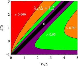

The upper panel of Fig. 2 shows the normal incident transmission probability as a function of and . The (black) diagonal strip is the region of perfect reflection, which occurs due to dominant Rashba effect. With fixing and decreasing , the reflection probability decreases as shown in the lower panel of Fig. 2. In the figure all the lines go through the point being , namely perfect transmission always occurs, because the Dirac cone appears again at the balanced Rashba and intrinsic SO case (). Further decreasing , the transmission probability decreases and reaches to zero at . Crossover from perfect reflection to perfect transmission occurs due to the competition between Rashba and intrinsic SO in the normal incident case.
IV.3 Charge conductance
Let us consider the rectangular geometry (Fig. 1) with infinite aspect ratio , and being respectively the width and length. We have considered so far the charge current carried by a single scattering channel with definite . In the absence of disorder, the channels are independent and the charge conductance (in units of ) is simply the sum of the single-channel transmissions over all possible transverse momenta , or equivalently over all incidence angles:
| (37) |
We evaluate Eq. (37) explicitly by substituting , where the reflection amplitude follows from the continuity condition (23). Note because of potential difference between the incident and transmitted side. The obtained charge conductance is shown in Fig. 3 as a function of for different values of . The curves exhibit specific features depending on the value of . We leave further inspection of such behaviors to Sec. III C.
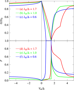
Fig. 3 shows several conductance curves as a function of for different values of . The incident energy is set to be . The conductance is normalized by where is the Fermi wavevector in the incident side.
IV.3.1 Semimetalic phase ()
When (Fig. 3(a), red curve), the system is in the semimetallic phase. The charge neutrality (particle-hole symmetric) point on the transmitted side is located at . The conductance vanishes at this point. Above this value of , the conductance shows a singularity at (discontinuity in the first derivative). Here, the Fermi energy touches the lowest energy band: on the transmitted side. Above this value, the number of energy bands contributing to the conductance is doubled. The conductance shows an abrupt increase of slope (a kink) at this point (see also Appendix).
Below the neutrality point (), the conductance shows a peak at , then turns to a slow and monotonic decrease as is decreased. This feature does not seem to resemble its behavior above the neutrality point. Decreasing from , the Fermi energy touches the highest energy band: at . But the conductance curve does not show any singularity here.
This asymmetric behavior is a fingerprint of the unique band structure of Kane-Mele model. At , the band touching the Fermi energy has the same band index , consequently the same symmetry as the incident state: . Therefore, as soon as this state becomes available for transport, transmission occurs, typically, at the normal incidence, leading to an abrupt increase of the conductance. On the other hand, at , the band touching the Fermi surface has the symmetry opposite to that of the incident state. Therefore, no transmission occurs at the normal incidence via the band, and the conductance curve bears only a gradual change. (see also Appendix A).
Note also that perfect reflection in the semimetallic phase is limited to normal incidence, and the conductance takes generally a finite value due to contribution from non-zero incident angle, , to the r.h.s. of Eq. (37). In the case of bilayer graphene, the conductance curve shows similar features, with two shoulders only on the side.
IV.3.2 Topological gap phase ()
When (Fig. 3(c), blue curve), the system bears a band gap. Naturally, the conductance vanishes identically in the gap region: , i.e., . The band is always activated for transport in the -regime: , showing no singular behavior in the conductance curve.
IV.3.3 At the phase boundary ()
At the phase boundary (Fig. 3(b), green curve), two bands with are combined, and a pair of linearly dispersing energy bands, i.e., a Dirac cone appears. The conductance curve is similar to that of monolayer graphene without spin-orbit interaction. Cayssol et al. (2009) The conductance vanishes at the charge-neutrality point , and shows again no singularity on the -side
IV.4 Fano factor
Fano factor associated with the potential step is obtained Cayssol et al. (2009) from the transmission probability as
| (38) |
The lower panel of Fig. 3 shows the Fano factor as a function of for different values of . One of the specific features is that the Fano factor shows, independently of the value of , a peak structure at , with a maximal value of (). This is, of course, partly related to the fact that the conductance vanishes at this point. However, recall also that in monolayer graphene without SO interaction, the Fano factor remains structureless at the corresponding point Cayssol et al. (2009), with a value of . Such characteristic suppression of shot noise is spoiled by the SO effects, even when , where Dirac cone reappears. A zero of the conductance leads, trivially, to a peak in the Fano factor. Very contrastingly, the charge conductance is not qualitatively affected by the SO effects.
The Rashba dominant regime exhibits some anomalous features: a cusp in the conductance at for (case (d) in Fig. 3) and an enhancement of the Fano factor. in the regime of perfect reflection. This corresponds to for . In the region of perfect reflection, evanescent modes are dominant in transport at a finite incident angle. The Fano factor is enhanced by such evanescent modes. The Fano factor increases with the increase of Rashba SO coupling in this regime of perfect reflection. In the balanced case, (Fig. 3(e)), the conductance curves do not differ significantly from the case of no SO effects (). In contrast, when intrinsic SO coupling dominates the Rashba term, i.e., in Fig 3(f), the conductance vanishes within a finite range of , corresponding to the gap. The Fano factor is not well-defined, therefore, not plotted in this regime of .
In the large and small enough potential region and for arbitrary , the Fano factor takes a value , which is roughly the same as the Fano factor without SO effects, since the transmitted state is free from evanescent modes in this region.
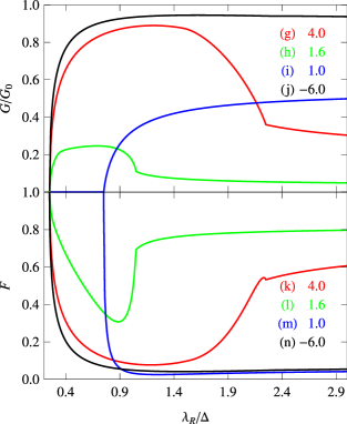
IV.5 Crossover effects in conductance and Fano factor
The charge conductance and the Fano factor are shown in Fig. 4 as a function of Rashba SO coupling . At normal incidence, we have seen a crossover from perfect reflection to perfect transmission in the -regime: (curves (i) and (ii) in the lower panel of Fig. 2). As for transport properties, perfect transmission at normal incidence is replaced by a broad maximum near (see cases (g) and (h) in the upper panel of Fig. 4). The maximum always appears in the -regime. However, unlike the normal incident case, the maximum of charge conductance is not unity and is not precisely located at as a consequence of angular integration.
The charge conductance becomes smaller with the decrease of the on the -side (e.g., cases (g) and (h) in the upper panel of Fig. 4), and actually vanishes at (not plotted). This is because the number of propagating states on the transmitted side reduces with the decrease of the (and vanish at ). A cusp of conductance appears also appears in this regime at the band edge of . When is larger than this value, the Fermi energy intersects with only band. As a result, perfect reflection occurs at the normal incidence, leading to smaller values of conductance.
On the other side, i.e., in the -regime: (e.g., cases (i) and (j)), maximum does not appear, because perfect reflection does not occur at the normal incidence (see (iii) and (iv) in the lower panel of Fig. 2). When (case (i)) , charge conductance vanishes in , where the system is gapped on the transmitted side.
Dependence of Fano factor on Rashba SO coupling is shown in the lower part of Fig. 4. Interestingly, the lower panel looks almost the upside down image of the upper panel.
V Spin transport
Here we investigate the spin transport generated by an electrostatic potential step in the presence of spin-orbit effects. The potential step splits the graphene sample in two pieces characterized by distinct carrier densities. The spin is drifted along the interface and the spin current is therefore transverse to the applied electric field. This spin Hall effect (SHE) is a mesoscopic analog of the bulk spin Hall effect occurring in homogeneous electron or hole doped semiconductors Murakami et al. (2003); Sinova et al. (2004). The present effect requires both spin-orbit coupling and a step in the carrier density. The spin Hall current localized in the vicinity of interface appears also in 2DEG with Rashba spin-orbit interaction Adagideli and Bauer (2005).
V.1 Local spin current density
The spin flows along the -axis, namely along the interface defined by the potential step. The total spin current density,
| (39) |
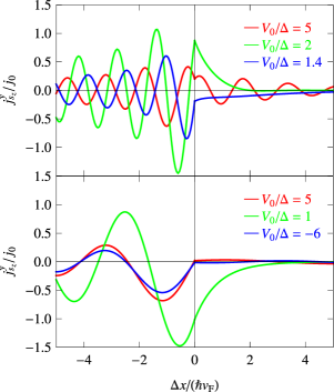
results from the summation of the single-channel currents over all possible transverse modes labeled by their momenta . This local current is maximal near the interface and decays when the distance is increased (Fig. 5). Note that the spacial dependence of spin current density is determined by a subtle interplay between the direct and cross terms. When both transmitted waves are propagative, the (singlechannel) crossed spin current oscillates as a function of the distance from the interface. Of course, these oscillations are damped when integrated over all possible transverse momenta (see Fig. 5) but this decay is a lonf ranged power law rather than an exponential decay.
When one or two transmitted wave(s) is/are evanescent, even the singlechannel current decays exponentially when the distance from the interface is increased. As a result, the total spin current density decays very abruptly with (see Fig. 5).
V.2 Spin conservation
The same situation occurs for the -component of spin current which comes only from the cross term, i.e. from Eq. (28). Moreover this contribution, due to spin torque in the presence of Rashba SO coupling, vanishes after integration over incident angle. The spin transport occurs, therefore, only in the direction parallel to the interface. Besides, the continuity of spin current-density is recovered after this angular averaging:
The spin current density, defined as Eq. (10), is thus considered to be a conserved quantity in the sense of Eq. (12), and free from the usual issue of defining a spin current.
V.3 Results
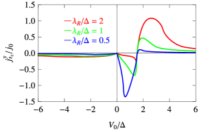
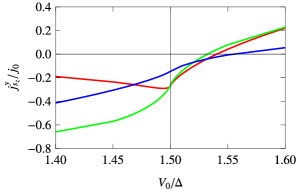
Fig. 5 shows the spatial distribution of spin current density parallel to the interface, i.e., -component of spin current is plotted as a function of coordinate normal to the interface for different values of Rashba SO coupling: (dominant Rashba phase) for the upper panel of Fig. 5, and (topological gap phase) for the lower panel Fig. 5.
In the upper panel, corresponds to the regime of perfect reflection, and the absolute value of spin current is large compared with other cases. The spin current is localized in the vicinity of interface, explicitly manifesting that spin is carried by evanescent modes (localized in the -direction but propagating in the -direction). It also shows a damped oscillatory behavior for a larger value of such as in the upper panel. Such damped oscillation is an incarnation of cross terms between evanescent and propagating modes. The lower panel of Fig. 5 corresponds to the topological gap phase, in which the spin current takes a large negative value when Fermi energy is in the gap on the transmitted side.
Fig. 6 shows spin Hall current at . Let us compare it with the charge conductance shown in Fig. 3, both represented as a function of . The two curves show indeed quite contrasting behaviors. At (in the absence of a junction) the charge conductance show a maximum (peak). In contrast, the spin current vanishes at , reflecting the fact that here, spin transport is a mesoscopic effect due to the presence of interface.
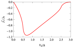
Both magnitude and sign of the spin current is tuned by . The direction of spin current is opposite between inter-band tunneling () and intra-band tunneling () cases (compare the two panels of Fig. 6). 111Some anomalous behaviors can be seen in the vicinity of , though. The latter includes also the case of metal-insulator junction. We can confirm this explicitly from Eqs. (18) and (28) with . The direct term of spin Hall current is proportional to , therefore the direction changes near . The sign of the crossed term is opposite from the direct terms and enhanced in the vicinity of Dirac point , resulting finite spin current at .
In the dominant Rashba phase (), two quadratic bands touch at the neutrality point . On the transmitted side, this corresponds to . At this value of , the charge conductance vanishes. The spin conductance changes its sign in the vicinity of neutrality point, but remains finite precisely on that point (see the lower panel of Fig. 6). This is again due to the evanescent modes. The spin current takes a large positive value above the neutrality point: . In the topological gap phase (), the charge conductances vanishes in the gap: , whereas the spin current is enhanced in the gap, taking a large negative value.
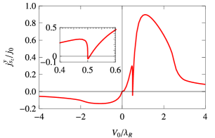
The upper panel of Fig. 7 reveals two different natures of mesoscopic spin Hall effect by studying, separately, the and cases. Fig. 7 shows that the mesoscopic spin Hall current flows actually in the absence of topological mass term: . The spin Hall current is enhanced in the regime of perfect reflection: ( in Fig. 7). This corresponds to the regime of above the neutrality point, where the spin conductance takes a large positive value. The lower panel of Fig. 7 shows, on contrary, as a function of in the absence of Rashba SOC: . Clearly, the spin current is enhanced, when Fermi energy is in the gap on the transmitted side: ( in Fig. 7), i.e., in the situation of metal-insulator junction. In the region of and , the spin current vanishes because only propagating mode appears. The spin degeneracy remains in the absence of Rashba SOC, as a result, the crossed term also vanishes.
On the transmitted side, the enhancement of spin Hall current thus occurs for two reasons: (i) perfect reflection in the dominant Rashba phase (on the side), (ii) due to the topological gap (on the side). In the two cases, evanescent modes play a dominant role in the solution of scattering problem at the junction. The enhancement of spin Hall current along the interface thus has two different natures, both related to evanescent modes. Depending on which side of the neutrality point Fermi energy on the transmitted side is, the enhanced spin current flows in the opposite directions.
VI Electron Veselago lensing
The junction in graphene is expected to serve as an electronic version of ”Veselago lens” Cheianov et al. (2007). The charge current distribution: , can be used for imaging the electronic flow around the potential step Cserti et al. (2007).
Let us imagine an electronic wave packet emitted from a point with . If the wave packet has a center-of-mass momentum with , then the wave packet will be incident at the junction (located at ) at . Let us consider the trajectory of this wave packet after it goes through the -junction.
Here, instead of following explicitly the dynamics of such a wave packet, we calculate directly the stationary charge current distribution on the transmitted side, using Eq. (24). Then, we consider stream lines of the vector field . Once is known, the following differential equation:
| (40) |
determines the locus of a stream line under a given boundary condition, say, . Equation (40) determines, in turn, the trajectory of the wave packet emitted from . As we have seen in Eqs. (13), (14), (15), (16), (III.3), has no -dependence, whereas has no spatial dependence due to charge conservation. Therefore, with a given boundary condition, Eq. (40) can be trivially integrated to give,
| (41) |
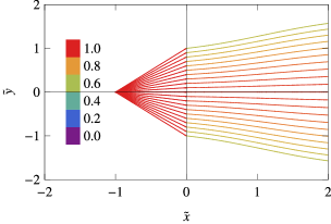
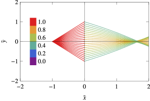
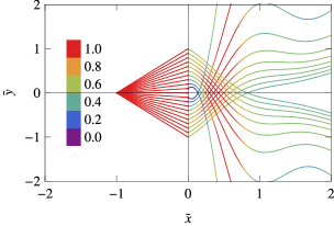
Repeating the same procedure for different values of incident angle , one can draw a set of stream lines visualizing the vector field . Focusing of such stream lines can be regarded as an electronic version of optical lens. Figs. 8 and 9 demonstrate such electron lens realized at the Kane-Mele junction. A color code specifies the strength of current flow along each trajectory.
VI.1 Topological gap phase
In the topogical gap phase, the refraction properties are quite similar to the ones studied previously for graphene junctions in the absence of spin-orbit interaction Cheianov et al. (2007). Indeed the -component of the current density changes its sign on crossing the junction, thereby realizing the negative or Veselago-like electronic refraction. In presence of SOC, the system does not longer show perfect focusing (Fig. 8.b).
In contrast for a junction (intraband transmission) the -component of the current has the same sign on both sides of the junction, indicating that the refractive index is positive. As a result, the outgoing electron beam is divergent (Fig. 8.a).
VI.2 Semimetallic phase
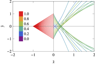
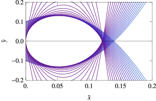
More interesting are the refraction properties of the semimetallic phase. Indeed the evanescent modes manifest themselves by the bending of the electronic rays on the transmitted side (Fig. 9). Moreover no transmission is allowed at the normal incidence which yields a shade area behind the origin O (Fig. 9).
Figure 9 shows Veselago-like electron lens in the semimetallic phase () for two distinct steps : (a) (left panel), (b) (right panel), both corresponding to a junction (inter-band tunneling).
In case (b), the Fermi energy is touching the top of -band, which happens when . As the Fermi energy approaches the the top of -band, the cross term between propagating (due to -band) and evanescent (due to -band) modes plays a significant role. The meandering stream lines in case (b) is a consequence of such ”cross term transport”. It should be also noticed that the shade area is much pronounced in case (b). Indeed, one can observe that the refractive index turns to be positive in the vicinity of the shade area. Due to perfect reflection at the normal incidence, the -component of current density is virtually zero for a small incident angle . As a result, the electron beam is strongly refracted, with divergent on the transmitted side (as ). This leads to the formation of shade area (see Fig. 10 for detailed plots).
Study of electron lens behavior thus reveals rich mesoscopic transport properties of the Kane-Mele -junction. It should be underlined that this unique mesoscopic transport is carried out by the evanescent modes and the cross terms. The former enables transport along the edge even when the Fermi level is in the gap on the transmitted side Yampol’skii et al. (2009).
VII Conclusion
We have studied theoretically charge and spin transport at a potential step (both and junctions) within the Kane-Mele of graphene. We have highlighted the role of reflection symmetry associated with the band index in the crossover from perfect reflection to transmission while tuning the Rashba coupling . We have also computed experimentally measurable quantities such as conductance and Fano factor.
Due to the multiband character of the model, one incident electron yields two distinct transmitted quasiparticles. The spin Hall current, which is mainly localized in the vicinity of interface, results from the superposition of two types of contributions: (i) direct terms involving one kind of transmitted quasiparticles and (ii) cross terms describing interferences between the two kinds of transmitted quasiparticles (Sec V). The direct terms were shown to carry no net -spin current when associated with a propagative wave whereas evanescent waves carry a finite spin current. In contrast the crossed terms always contribute to spin transport regardless of the nature of the waves.The interplay between those direct and cross terms is also important for charge transport (Sec. IV).
Moreover the electronic flow exhibits a large variety of patterns (Sec. VI). In particular a dominant Rashba SOC (semimetallic phase) leads to curved rays owing to the presence of evanescent states whereas rays are still straight for dominant intrinsic SOC (topological gap phase). Note that in a monolayer graphene without SOC, stream lines are straight and refracted only at the interface. In principle, it should be possible to identify those contrasted shapes by scanning a charged tip above the graphene flake as it was performed for two-dimensional electron gases in GaAs heterostructures Topinka et al. (2000, 2001). Finally detecting a clear fingerprint of the role of SOC in transport measurements in graphene seems not impossible but difficult, since the magnitude of SOC is small in graphene, at most, on the order of . Gmitra et al. (2009). An alternative way to probe such unique transport characteristics of junction may be to use materials with stronger SOC, such as HgTe/CdTe heterostructures.
Acknowledgements.
K.I. and A.Y. are supported by KAKENHI (K.I.: Grant-in-Aid for Young Scientists under Grants No. B-19740189 and A.Y.: No. 08J56061 of MEXT, Japan). JC is supported by the 7th European Community Framework Programme under the contract TEMSSOC (joint program between UC Berkeley and the Max-Planck-Institut f r Physik Komplexer Systeme in Dresden). *

Appendix A Asymptotic Behavior of Conductance
The curve of in Fig. 3 illustrates the characteristic features of charge conductance in the semimetallic phase: . The conductance curve shows, say, at , a kink structure at , on opening of the -channel to transmission. The purpose of this appendix is to estimate the asymptotic behavior of in the vicinity of this singularity.
In Sec. IV.3 we estimated , by substituting with determined by the continuity condition (23), into the Landauer formula (37). Here, to reveal the nature of singularity at , we extract the contribution of -band to , and analyze its asymptotic behavior in the vicinity of the singularity (see Fig. 11). Let us introduce , the height of potential barrier measured from the singularity:
| (42) |
When , the -band gives no contribution to the charge current on the transmitted side, since the state is evanescent. When , a propagating mode becomes possible with the momentum
| (43) |
obtained from the energy conservation: , provided , where the critical angle is defined by,
| (44) |
In the limit of , this reduces to,
| (45) |
The charge current transmitted to the lowest energy band is given by
| (46) |
from Eq. (13). Integrating over all incident angles, one finds
| (47) |
The charge current transmitted to the -band thus shows a linear uprise (proportional to ) when . As a result, the charge conductance shows an abrupt increase of slope at . Note that thanks to the same symmetry, i.e., the same (), of the -band as that of the incident energy band: .
Similarly, we investigated the asymptotic behavior of in the vicinity of the opening of -channel at . However, since the -band (final state) has the opposite symmetry (opposite ) to the initial state: . Due to this mismatch of symmetry, transmission coefficient vanishes even when . As a result, the leading order contribution to the charge conductance starts at second order, i.e., (see Fig. 11, right panel).
References
- Murakami et al. (2003) S. Murakami, N. Nagaosa, and S.-C. Zhang, Science 301, 1348 (2003).
- Sinova et al. (2004) J. Sinova, D. Culcer, Q. Niu, N. A. Sinitsyn, T. Jungwirth, and A. H. MacDonald, Phys. Rev. Lett. 92, 126603 (2004).
- Kato et al. (2004) Y. K. Kato, R. C. Myers, A. C. Gossard, and D. D. Awschalom, Science 306, 1910 (2004).
- Wunderlich et al. (2005) J. Wunderlich, B. Kaestner, J. Sinova, and T. Jungwirth, Phys. Rev. Lett. 94, 47204 (2005).
- Kane and Mele (2005a) C. L. Kane and E. J. Mele, Phys. Rev. Lett. 95, 226801 (2005a).
- Kane and Mele (2005b) C. L. Kane and E. J. Mele, Phys. Rev. Lett. 95, 146802 (2005b).
- Bernevig et al. (2006) B. A. Bernevig, T. L. Hughes, and S.-C. Zhang, Science 314, 1757 (2006).
- König et al. (2008) M. König, H. Buhmann, L. W. Molenkamp, T. L. Hughes, C. X. Liu, X.-L. Qi, and S.-C. Zhang, J. Phys. Soc. Jpn. 77, 031007 (2008).
- Qi and Zhang (2010a) X.-L. Qi and S.-C. Zhang, Physics Today 63, 33 (2010a).
- Moore (2010) J. E. Moore, Nature 464, 194 (2010).
- Hasan and Kane (2010) M. Z. Hasan and C. L. Kane (2010), eprint arXiv:1002.3895.
- Qi and Zhang (2010b) X.-L. Qi and S.-C. Zhang (2010b), eprint arXiv:1002.2026.
- König et al. (2007) M. König, S. Wiedmann, C. Brüne, A. Roth, H. Buhmann, L. W. Molenkamp, X.-L. Qi, and S.-C. Zhang, Science 318, 766 (2007).
- Roth et al. (2009) A. Roth, C. Brüne, H. Buhmann, L. W. Molenkamp, J. Maciejko, X.-L. Qi, and S.-C. Zhang, Science 325, 294 (2009).
- Min et al. (2006) H. Min, J. E. Hill, N. A. Sinitsyn, B. R. Sahu, L. Kleinman, and A. H. MacDonald, Phys. Rev. B 74, 165310 (2006).
- Huertas-Hernando et al. (2006) D. Huertas-Hernando, F. Guinea, and A. Brataas, Phys. Rev. B 74, 155426 (2006).
- Yao et al. (2007) Y. Yao, F. Yei, X. L. Qi, S.-C. Zhang, and Z. Fang, Phys. Rev. B 75, 041401 (2007).
- Yamakage et al. (2009) A. Yamakage, K.-I. Imura, J. Cayssol, and Y. Kuramoto, Eur. Phys. Lett. 87, 47005 (2009).
- Huard et al. (2007) B. Huard, J. A. Sulpizio, N. Stander, K. Todd, B. Yang, and D. Goldhaber-Gordon, Phys. Rev. Lett. 98, 236803 (2007).
- Williams et al. (2007) J. R. Williams, L. DiCarlo, and C. M. Marcus, Science 317, 638 (2007).
- Özyilmaz et al. (2007) B. Özyilmaz, P. Jarillo-Herrero, D. Efetov, D. A. Abanin, L. S. Levitov, and P. Kim, Phys. Rev. Lett. 99, 166804 (2007).
- Oostinga et al. (2008) J. B. Oostinga, H. B. Heersche, X. Liu, A. F. Morpurgo, and L. M. K. Vandersypen, Nature Mat. 7, 151 (2008).
- Gorbachev et al. (2008) R. V. Gorbachev, A. S. Mayorov, A. K. Saychenko, D. W. Horsell, and F. Guinea, Nano Lett. 8, 1995 (2008).
- Liu et al. (2008) G. Liu, J. J. Velasco, W. Bao, and C. N. Lau, Appl. Phys. Lett. 92, 203103 (2008).
- Katsnelson et al. (2006) M. I. Katsnelson, K. S. Novoselov, and A. K. Geim, Nature Phys. 2, 620 (2006).
- Cheianov and Falko (2006) V. V. Cheianov and V. I. Falko, Phys. Rev. B 74, 041403 (2006).
- Cayssol et al. (2009) J. Cayssol, B. Huard, and D. Goldhaber-Gordon, Phys. Rev. B 79, 075428 (2009).
- Huard et al. (2008) B. Huard, N. Stender, J. A. Sulpizio, and D. Goldhaber-Gordon, Phys. Rev. B 78, 121402 (2008).
- Stander et al. (2009) N. Stander, B. Huard, and D. Goldhaber-Gordon, Phys. Rev. Lett. 102, 026807 (2009).
- Dyrdałet al. (2009) A. Dyrdał, V. K. Dugaev, and J. Barnaś, Phys. Rev. B 80, 155444 (2009).
- Murakami et al. (2004) S. Murakami, N. Nagaosa, and S.-C. Zhang, Phys. Rev. B 69, 235206 (2004).
- Adagideli and Bauer (2005) I. Adagideli and G. E. W. Bauer, Phys. Rev. Lett 97, 256602 (2005).
- Cheianov et al. (2007) V. V. Cheianov, V. Fal’ko, and B. L. Altshuler, Science 315, 1252 (2007).
- Cserti et al. (2007) J. Cserti, A. Palyi, and C. Peterfalvi, Phys. Rev. Lett 99, 246801 (2007).
- Yampol’skii et al. (2009) V. A. Yampol’skii, S. S. Apostolov, Z. A. Maizelis, A. Levchenko, and F. Nori (2009), eprint arXiv:0903.0078.
- Topinka et al. (2000) M. Topinka, B. LeRoy, S. Shaw, E. Heller, R. Westervelt, K. Maranowskik, and A. Gossard, Science 289, 2323 (2000).
- Topinka et al. (2001) M. Topinka, B. LeRoy, R. Westervelt, S. Shaw, R. Fleischmann, E. Heller, K. Maranowskik, and A. Gossard, Nature 410, 183 (2001).
- Gmitra et al. (2009) M. Gmitra, S. Konschuh, C. Ertler, C. Ambrosch-Draxl, and J. Fabian, Phys. Rev. B 80, 235431 (2009).