Forward Instrumentation for ILC Detectors
Abstract
Two special calorimeters are foreseen for the instrumentation of the very forward region of the ILC detector, a luminometer designed to measure the rate of low angle Bhabha scattering events with a precision better than 10-3 and a low polar angle calorimeter, adjacent to the beam-pipe. The latter will be hit by a large amount of beamstrahlung remnants. The amount and shape of these depositions will allow a fast luminosity estimate and the determination of beam parameters. The sensors of this calorimeter must be radiation hard. Both devices will improve the hermeticity of the detector in the search for new particles. Finely segmented and very compact calorimeters will match the requirements. Due to the high occupancy fast front-end electronics is needed. The design of the calorimeters developed and optimised with Monte Carlo simulations is presented. Sensors and readout electronics ASICs have been designed and prototypes are available. Results on the performance of these major components are summarised.
keywords:
Forward Calorimeters, ILC Detector, Luminosity Measurement, Radiation Hard Sensors, FE ASICs1 Introduction and challenges
A high energy e+e- linear collider is considered to be the future research facility complementary to the LHC collider. Whereas LHC has a higher potential for discoveries, an e+e- collider will allow precision measurements to explore in detail the mechanism of electroweak symmetry breaking and the properties of the physics beyond the Standard Model, should it be found at the LHC. Two concepts of an e+e- linear collider are presently considered, the ILC [1] and CLIC [2]. For the ILC, with superconducting cavities, an engineering design report will be issued in 2012. The centre-of-mass energy will be 500 GeV, with the possibility of an upgrade to 1 TeV. CLIC is based on conventional cavities. A conceptional design report is foreseen in 2011. CLIC will allow to collide electrons and positrons up to energies of 3 TeV.
An R&D program is ongoing to develop the technologies for detectors for precision measurements in this new energy domain. Letters of Intent have been submitted for detectors at the ILC in 2009. Two detectors, the ILD [3] and the SiD [4], are reviewed and validated. In both detectors two specialised calorimeters are foreseen in the very forward region, LumiCal for the precise measurement of the luminosity and BeamCal for a fast estimate of the luminosity and for the control of beam parameters [5]. Both will also improve the hermeticity of the detector. To support beam-tuning an additional pair-monitor will be positioned just in front of BeamCal.
With LumiCal the luminosity will be measured using Bhabha scattering, , as a gauge process. To match the physics benchmarks, an accuracy of better than 10-3 is needed at a centre-of-mass energy of 500 GeV [3]. For the GigaZ option, where the ILC will be operated for precision measurements at centre-of-mass energies around the Z boson, an accuracy of 10-4 would be required [6]. To reach these accuracies, a precision device is needed, with particularly challenging requirements on the mechanics and position control.
BeamCal is positioned just outside the beam-pipe. At ILC energies we have to tackle here a new phenomenon – the beamstrahlung. When electron and positron bunches collide, the particles are accelerated in the magnetic field of the bunches towards the bunch centre. This so called pinch effect enhances the luminosity. However, electrons and positrons may radiate photons. A fraction of these photons converts in the Coulomb field of the bunch particles creating low energy pairs. A large amount of these pairs will deposit their energy after each bunch crossing in BeamCal. These depositions, useful for a bunch-by-bunch luminosity estimate and the determination of beam parameters [7], will lead, however, to a radiation dose of about one MGy per year in the sensors at lower polar angles. Hence radiation hard sensors are needed to instrument BeamCal. BeamCal is supplemented by a pair monitor, consisting of a layer of pixel sensors positioned just in front of it to measure the density of beamstrahlung pairs and give additional information for the beam parameter determination.
All detectors in the very forward region have to tackle relatively high occupancy, requiring special front-end electronics.
A small Molière radius is of importance for both calorimeters. It ensures high energy electron veto capability for BeamCal even at small polar angles. This is essential to suppress background in searches for new particles for which the signature consists of large missing energy and momentum. In LumiCal the precise reconstruction of electron, positron and photon showers in Bhabha events is facilitated. Both calorimeters also shield the inner tracking detectors from back-scattered particles induced by beamstrahlung pairs hitting the downstream beam-pipe and magnets.
2 Design of the very forward region
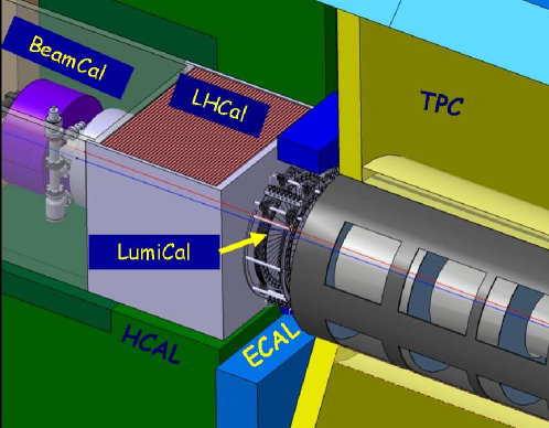
A sketch of the very forward region of the ILD detector [3] is shown in Figure 1. LumiCal and BeamCal are designed as cylindrical sensor-tungsten sandwich electromagnetic calorimeters. Both consist of 30 absorber disks of 3.5 mm thickness, each corresponding to one radiation length, interspersed with sensor layers. Each sensor layer is segmented radially and azimuthally into pads. Front-end ASICs are positioned at the outer radius of the calorimeters. LumiCal is positioned in a circular hole of the end-cap electromagnetic calorimeter ECAL. BeamCal is placed just in front of the final focus quadrupole. BeamCal covers polar angles between 5 and 40 mrad and LumiCal between 31 and 77 mrad.
Colliding beams enter the interaction point, IP, with a crossing angle of 14 mrad. Both calorimeters are centred around the outgoing beam. In the design of BeamCal a hole for the incoming beam-pipe is foreseen.
2.1 LumiCal simulation studies
The differential cross section of Bhabha scattering, , can be calculated precisely from theory [8]. In leading order it reads,
| (1) |
where is the polar angle of the scattered electron with respect to the beam. The approximation holds at small .
For a given rate of Bhabha events, NB, determined in a certain -range, the luminosity, , is obtained as
| (2) |
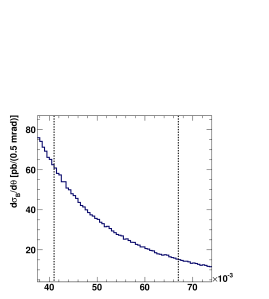
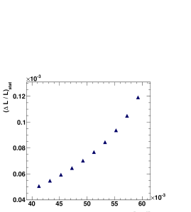
where is the integral of the differential cross section, eqn. (1), over the considered range. Because of the steep dependence of the cross section, as illustrated in Figure 2a, the most critical quantity to control when counting Bhabha events is the inner acceptance radius of the calorimeter, defined as the lower cut in the polar angle, . Hence a very precise measurement is needed. Furthermore, the -range must be chosen such that the number of Bhabha events measured provides the required relative statistical uncertainty of 10-3. By choosing the lower bound of the polar angle between 40 and 60 mrad the latter requirement can be easily reached as illustrated in Figure 2b. Here a Bhabha event sample generated with the BHWIDE generator [9] was used. The generated sample corresponds to an integrated luminosity of 500 fb-1, as expected in one year of running the collider at nominal luminosity.
Electromagnetic showers are simulated in LumiCal using the GEANT4 [10] based package Mokka [11]. Sensors consist of 300 m thick silicon sectors covering an azimuthal angle of 30∘. The depositions in each sensor pad are recorded, and a reconstruction of the shower is performed. The position of an electromagnetic shower in LumiCal is reconstructed by performing a weighted average over the energy deposits in individual pads. The weight, , of a given detector pad i is determined by logarithmic weighting [12], for which . Here refers to the individual pad energy, is the total energy in all pads, and is a constant. In this way, only pads which contain a sufficient fraction of the shower energy contribute to the reconstruction. The polar angle resolution, , and a polar angle measurement bias, , are defined as the Gaussian width and the central value of the difference between the reconstructed and the generated polar angles. There is an optimal value for , for which is minimal [13, 14].
Non-zero values of are due to the non-linear signal sharing on finite size pads with gaps between them. The bias and the resolution in the polar angle measurement depend on the polar angle pad size. The bias causes a shift in the luminosity measurement, since events may migrate into or out of the fiducial volume. This shift reads as
| (3) |
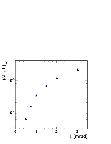
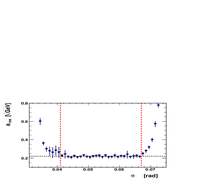
Figure 3a shows the relative shift in the luminosity as a function of the polar angular pad size, lθ, using the optimal value of . For l mrad the shift in the luminosity measurement is smaller than . As the baseline for the design we have chosen l mrad, which corresponds to 64 radial divisions of the sensor. For this segmentation the polar angle resolution and bias amount to and mrad, respectively. The relative shift in the luminosity is .
The polar angle bias needs careful understanding in test-beam measurements with sensors finally chosen for the calorimeter. Once its value is known, a correction can be applied to the luminosity measurement. The uncertainty of the luminosity measurement is then given by the uncertainty of the measured bias which may be smaller than the shift itself. The value of can therefore be considered as an upper bound on the relative luminosity bias.
With 30 radiation lengths of tungsten as absorber, high energy electrons and photons deposit almost all of their energy in the detector. The relative energy resolution, , is parametrised as
| (4) |
where and are, respectively, the central value and the standard deviation of the distribution of the energy deposited in the sensors for a beam of electrons with energy . The parameter is usually quoted as the energy resolution, a convention which will be followed here.
Figure 3b shows the energy resolution as a function of the polar angle for electron showers with energy 250 GeV. The energy resolution parameter approaches minimal constant values between = 41 mrad and = 67 mrad, where the shower is fully contained inside the calorimeter. The fiducial volume of LumiCal is thus defined to be the polar angular range
| (5) |
as indicated by the dashed lines in Figure 2a. Fiducial cuts on the minimal and maximal reconstructed polar angles of the particles used for the luminosity measurement reject events with shower leakage through the edges of LumiCal. For electron showers located inside the fiducial volume of LumiCal, the energy resolution is estimated to be . No dependence on the electron energy is found in the energy range from 50 to 300 GeV. In order to determine the energy of showering particles, the integrated deposited energy in the detector has to be multiplied by a calibration factor. The calibration factor is found to be constant in the same energy range.
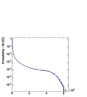
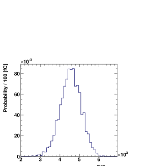
The expected range of energy depositions in the pads has been studied for the passage of minimum ionising particles, hereafter denoted as MIPs, and for showers of 250 GeV electrons [15]. The energy deposition in silicon is converted to released ionisation charge. The distribution of the charge in a single pad, , is shown in Figure 4a. It ranges between fC. The distribution of the maximal charge collected in a single pad is shown in Figure 4b. About 95 % of electron shower signals are less than fC.
The impact of the digitisation of the detector signal on the LumiCal performance is investigated in Ref. [15]. It is shown that an ADC with 8 bit resolution is sufficient to keep the energy resolution quoted above. No bias in the energy measurement is found.
2.2 BeamCal simulation studies
BeamCal will be hit after each bunch-crossing by a large amount of beamstrahlung pairs. Their number, energy and spatial distribution depend on the beam parameters and the magnetic field inside the detector. For the nominal ILC beam-parameter set [16], beamstrahlung pairs are generated with the GUINEA-PIG program [17]. Inside the ILC detector an anti-DID field [18] is assumed. Beamstrahlung pairs are simulated in the detector, using a program based on GEANT4.
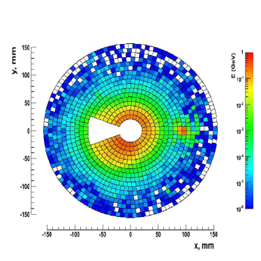
The energy deposited in the sensors of BeamCal per bunch crossing, about 150 GeV as shown in Figure 5a, and the shape of these depositions allow a bunch-by-bunch luminosity estimate and the determination of beam parameters [7]. From the spatial distribution of the deposited energy a set of observables, e.g. radial and angular moments and asymmetries, is defined. These observables are related to beam parameters like bunch sizes, emittances and bunch offsets by a matrix equation. In the single parameter determination accuracies better than 10% [7] are obtained. In the multiparameter mode correlations appear. However, reasonable precision can still be obtained by using information from other diagnostics devices.
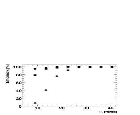
For search experiments it is important to detect single high energy electrons on top of the wider spread beamstrahlung pairs. Superimposed on the pair depositions in Figure 5a is the deposition of an electron of 250 GeV, seen as the red spot on the right side. By performing an appropriate subtraction of the pair deposits and a shower-finding algorithm which takes into account the longitudinal shower profile, high energy electrons can be detected with high efficiency, as shown in Figure 5b. This feature allows to suppress the background from two-photon processes in a search e.g. for super-symmetric tau-leptons [19] in a large fraction of the parameter space.
is assumed.
The range of signals expected on the pads was estimated. Including the depositions from beamstrahlung signals up to 40 pC are expected. Digitising the signals with an ADC with 10 bit resolution has no impact on the performance of the calorimeter.
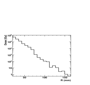
GEANT4 simulations are also used to determine the expected dose and the neutron fluence in the sensors after one year of operation with nominal beam parameters. The dose in a sensor layer at the depths of the shower maximum as a function of the radius is shown in Figure 6a. In the innermost ring of the calorimeter a dose of about 0.5 MGy is expected. Since the dose is non-uniformly distributed as a function of the azimuthal angle, it approaches 1 MGy per year in some sensor areas of the inner rings.
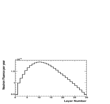
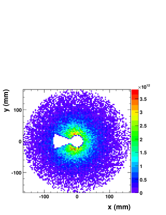
The neutron fluence is estimated using in GEANT4 the cascade model of Bertini [20]. The fluence per year of running at nominal beam parameters is shown in Figure 6b as a function of the sensor layer number. Fluences up to 21015 per layer are expected near the shower maximum. Other GEANT4 models predict lower neutron fluences, particularly at low neutron energies [21]. The distribution of the fluence of neutrons in the sensor layer with the maximum fluence is shown in Figure 7. With the cascade model of Bertini, a neutron fluence of 0.4 1012 neutrons per mm2 and year is expected near the beam-pipe. Albeit this is still an order of magnitude less than predicted for LHC detectors near the beam pipe dedicated tests of sensors are planned.
2.3 Pair monitor simulations
Additional and independent information on beam parameters will be obtained from the pair monitor [22, 23]. The device will consist of one layer of silicon pixel sensors, with pixel size of 400400 m2, just in front of BeamCal to measure the number density distribution of beamstrahlung pairs. Here we investigated the sensitivity to the horizontal and vertical bunch sizes, and , and the ratio of the vertical displacement between bunches crossing to their vertical size, .
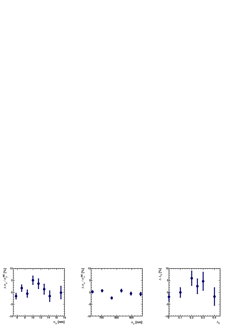
To reconstruct the beam profile several observables characterising the number density of pairs at the front face of BeamCal are used [24]. Bunch crossings are simulated for certain ranges of , and , and each of these observables is fitted with a second order polynomial. Then, several thousand bunch crossings are generated using different sets of beam parameters and , , and are reconstructed with the inverse matrix method. Figure 8 shows a few examples of the results displayed as the difference between the beam parameters reconstructed and set in the simulation divided by the latter, averaged over 50 bunch crossings. These quantities are compatible with zero. The relative uncertainties, averaged over about 100 such reconstructions of vertical and horizontal beam sizes and the relative vertical displacement are 10.1%, 3.2% and 8.0%, respectively.
3 Mechanical concepts
On the basis of the simulation results mechanical designs of both calorimeters are developed. To allow their installation after the beam-pipe is in place, both calorimeters consist of two half-cylinders. A schematic of a half cylinder of BeamCal is shown in Figure 9a.
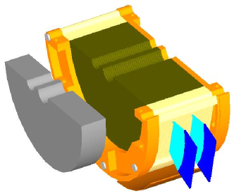
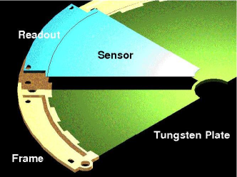
The tungsten absorber disks are embedded in a mechanical frame stabilised by steel rods. Each layer is composed of a tungsten half-disc surrounded by a brass half-ring as shown in Figure 9b. Precise holes in the brass ring will ensure a position accuracy of better than 100m. The sensors are fixed on the tungsten and connected via a flexible PCB to the front-end readout. The distance between two adjacent tungsten plates is kept to 1 mm to approach the smallest possible Molière radius. The sensors of BeamCal are structured into pads of about 88 mm2 size allowing the maximum electron detection efficiency [25]. Due to the required high radiation tolerance, GaAs sensors are foreseen. For the innermost part of BeamCal, adjacent to the beam-pipes, also CVD111Chemical Vapour Deposition diamond is considered.
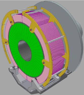
The design of LumiCal is similar [26]. Since it is a precision device, special care is devoted to the mechanical stability and position control. The tungsten half-discs are held by special bolts. For a half barrel structure as shown in Figure 10 a finite element simulation is performed. The calorimeter weight leads to a maximal vertical displacement of 20 m. For a temperature difference of 1 K over a disk, the deformation of the shape of the tungsten plate is estimated to be 25 m.
To match the requirements on the precision of the lower polar angle measurement, the sensor positions at the inner acceptance radius must be controlled to better than 40 m. Other critical quantities are the distance between the two calorimeters and the position of the beam with respect to the calorimeter axis. The former must be known to about 1 mm and the latter to 500 m. A laser based position monitoring system has been developed [27] to control the position of LumiCal over short distances with m precision.
For LumiCal, sensors made of high-ohmic n-type silicon are foreseen. The thickness of the sensors is about 300 m. The p+ side is segmented in polar and azimuthal pads and the backside is fully metallised. To keep the Molière radius small the gap for the sensors is 1 mm. The signals on the pads of both calorimeters are led by thin copper strips on a Kapton foil to the front-end electronics positioned at the outer radius of the calorimeter.
4 Systematic effects in the luminosity measurement
Several phenomena which may have an impact on the luminosity measurement are considered. These are: pinch effect and beamstrahlung, background from two-photon processes, the resolution and scale of the electron energy measurement and the beam polarisation.
4.1 Pinch effect and beamstrahlung
Due to the pinch effect the luminosity for given bunch charges and sizes will be enhanced. However, electrons and positrons may radiate photons prior to Bhabha scattering. In addition, final state particles are deflected inside the bunch. The result is a reduction of the Bhabha event counting rate in a given range of low polar angles. The reduction is found to depend on the selection criteria for Bhabha events. For a selection optimised for nominal ILC beam parameters at 500 GeV centre-of-mass energy, it amounts to 1.510.05% [28], where the quoted uncertainty stems from the statistics in the simulation. The dominant contribution to the loss is due to the reduction in the centre-of-mass energy caused by beamstrahlung. The latter leads to an effective centre-of-mass energy distribution called luminosity spectrum.
In the measurement of the luminosity, the loss of Bhabha events has to be corrected for. The impact of beamstrahlung can be estimated from the measured luminosity spectrum with a relative uncertainty of about 10-3 [28]. The impact of the deflection inside the bunch depends mainly on the horizontal bunch-size, , and the bunch length, . Assuming that one can control these two quantities with a relative uncertainty of 5%222In Ref. [7] the estimated uncertainty of e.g. varies between 0.5% and 6.5%, depending on the number of free beam parameters in the analysis. A similar range of precision is obtained for ., the uncertainty of a correction to the luminosity is about 1.5 10-3 [28].
4.2 Background from four-fermion production
Four-fermion production is known to have a large cross section with maxima at low polar angles.
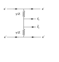
It is dominated by the diagram shown in Figure 11, where two virtual photons are exchanged between electron spectators. We used the WHIZARD [29] event generator to obtain samples of events for final states with leptons in the inner legs. The generator was tuned to experimental data of the process e+e e+e- c using data from LEP and other accelerators [30]. The cross-section of four–lepton production amounts to 12.00.5 nb at 500 GeV when the momenta of the exchanged photons are required to be larger than 0.1 GeV/c. The spectators remain at high energy. Less than 1% of them hit the luminosity calorimeter and become a background for Bhabha events. A Bhabha event sample has been generated with a cross-section of 4.700.03 nb at 500 GeV centre-of-mass energy, using the BHLUMI [31] event generator. The LumiCal response is simulated using BARBIE V4.3 [32], a GEANT3 based simulation program. The following event selection criteria are applied: the polar angle of the reconstructed shower must be within the LumiCal fiducial volume at one side and within mrad and – 7 mrad on the other. In addition, the total energy deposited in both calorimeters must be more than 80 of the center-of-mass energy. These criteria are optimised to reduce the impact of beamstrahlung and deflection on the Bhabha event counting to the amount given in the previous section [28]. The selection efficiency of Bhabha scattering events is about 68.
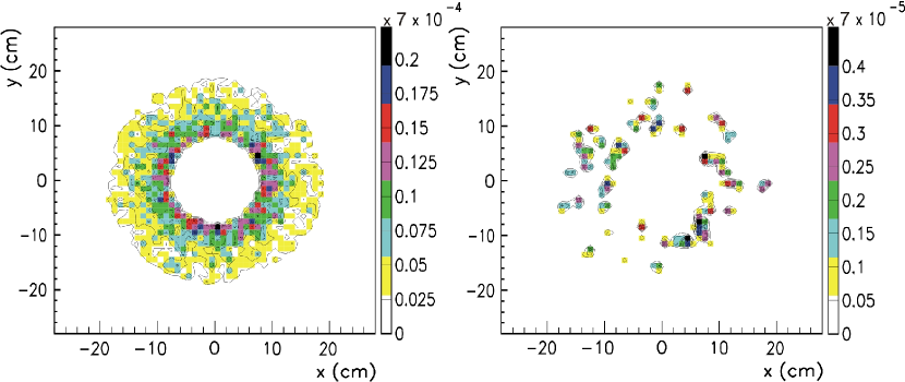
Four-fermion events in the LumiCal are to a large fraction rejected by the Bhabha selection criteria. This is illustrated in Figure 12 where the hits of particles from the four-fermion final states in the front plane of LumiCal per bunch crossing are shown before and after applying the Bhabha event selection. The fraction of four-fermion final states in the selected Bhabha event sample is 2.310-3.
At LEP energies agreement between measurements and modelling of four-fermion processes was obtained within 20% [30]. Assuming that at 500 GeV it will be possible to model these processes with a precision of 40%, correcting the luminosity measurement correspondingly will lead to an uncertainty of 0.910-3.
4.3 Effects of a bias in the energy resolution and the energy scale
One of the criteria to select Bhabha events is the total energy measured in the calorimeters, required to be larger than 80% of the centre-of-mass energy. A possible bias in the energy resolution or the energy calibration will result in a change of the number of selected Bhabha events and hence in the measured luminosity.
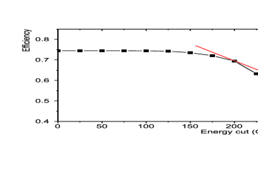
The selection efficiency for Bhabha events as a function of the required energy in the calorimeters is shown in Figure 13a. At the position of the cut in the measured calorimeter energy the slope of the tangent to the function is about –1.8. To keep the shift of the luminosity below , the cut in the measured calorimeter energy must be controlled with a precision of about 400 MeV. A study done allowing a constant offset in the measured energy leads to a similar requirement [33].
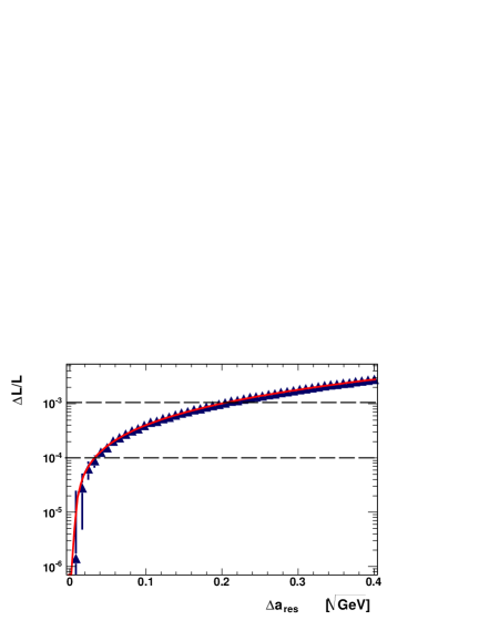
The effect of a bias in the energy resolution, in eqn. 4, is illustrated in Figure 13b. We estimate that if can be controlled within 20%, it will contribute to the luminosity uncertainty by about .
4.4 Impact of electron and positron polarisation
To exploit the full physics potential of a linear collider, electron and positron beams will be polarised. Polarisation will also change the Bhabha cross section in the acceptance range of LumiCal up to a few per cent [34]. In the current design the maximum values for electron and positron polarisation are 0.8 and 0.6, respectively, with an uncertainty of 0.0025 [35]. Using these values the shift in the Bhabha cross section is 2.310-2 with an uncertainty of 1.910-4.
4.5 Summary of systematic uncertainties
In addition to effects studied in this chapter also the impact of the polar angle resolution and polar angle bias as estimated in section 2.1 are included. All uncertainties based on the current level of understanding are summarised in Table 1. They are considered as being uncorrelated, leading currently to a total uncertainty of 2.3 10-3.
The estimated systematic uncertainties on the luminosity measurement from all sources considered above at a centre-of-mass energy of 500 GeV. Source Value Uncertainty Luminosity Uncertainty 2.210-2 100% 1.610-4 3.210-3 100% 1.610-4 0.21 15% 10-4 luminosity spectrum 10-3 bunch sizes , , 655 nm, 300 m 5% 1.510-3 two photon events 2.310-3 40% 0.910-3 energy scale 400 MeV 100% 10-3 polarisation, e-, e+ 0.8, 0.6 0.0025 1.910-4 total uncertainty 2.3 10-3
The reduction of the largest uncertainty, due to the deflections of final state electrons or positrons inside the bunch, needs further investigation. Also the energy scale uncertainty may be reduced by a proper calibration.
5 Sensor development
5.1 Sensors for BeamCal
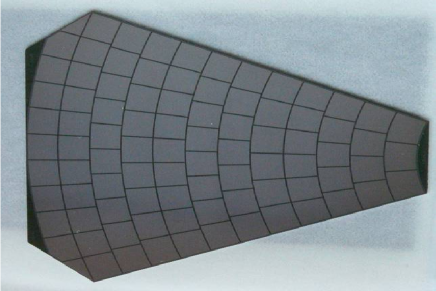
The challenge of BeamCal is to find sensors tolerating about one MGy of dose per year. So far polycrystalline CVD diamond sensors of 1 cm2 size and larger sectors of GaAs pad sensors, as shown in Figure 14, have been studied. Irradiation is done using a 10 MeV electron beam at the S-DALINAC accelerator [36]. The intensity is varied between 10 and 100 nA corresponding to dose rates between 10 and 200 kGy/h. Since large area CVD diamond sensors are extremely expensive, they may be used only at the innermost part of BeamCal. At larger radii GaAs sensors appear to be a promising option.
5.1.1 GaAs sensors
Large area GaAs sensors are obtained from the Tomsk State University. They are produced using the liquid encapsulated Czochralski method and are doped with tin and tellur as shallow donors and chromium as a deep acceptor.
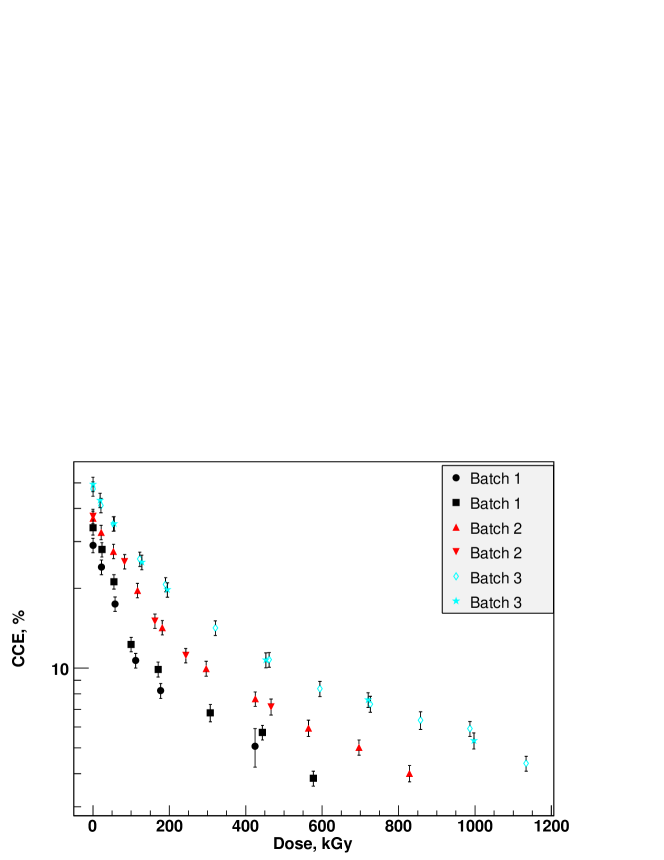
Three batches with different concentrations of dopants are irradiated up to 1.2 MGy and the charge collection efficiency, CCE, is measured as a function of the absorbed dose. The results are shown in Figure 15. The charge collection efficiency depends slightly on the dopant concentration. The sensors with a lower donor concentration show a larger initial charge collection efficiency and the decrease of the charge collection efficiency as a function of the absorbed dose is less steep. The smallest decrease of the CCE as a function of the dose is observed for tin donor. A MIP signal is separated from the pedestal up to a dose of 600 kGy for the sensors with lower donor concentration.
The leakage current of a pad at room temperature before irradiation is about 200 nA at an applied voltage of 50 V. After exposure of a dose of 1.2 MGy leakage currents of up to a factor 2 larger were found. The pad capacitance is measured to 12 pF. The results are consistent with previous measurements [37].
5.1.2 CVD diamond sensors
For polycrystalline diamond sensor samples of 1 cm2 area and 500 m thickness the linearity of the response and the leakage current and the signal collection efficiency have been investigated as a function of the absorbed dose [38]. The signal size depends linearly on the number of charged particles crossing the sensors for up to 5106 particles in 10 ns. The leakage current, less than 1 pA at room temperature, depends only slightly on the absorbed dose up to 7 MGy. The charge collection efficiency rises by a factor of two for doses between 0.5 to 1 MGy, then drops smoothly approaching the charge collection efficiency of a non-irradiated sensor. Provided the sensor is continuously irradiated, this efficiency is reached at about 7 MGy.
5.2 Sensors for LumiCal
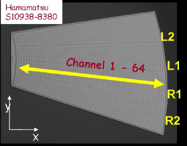
Prototypes of LumiCal sensors have been designed [39] and then manufactured by Hamamatsu Photonics. A picture of a sensor is shown in Figure 16. Its shape is a ring segment of 30∘. The thickness of the n-type silicon bulk is 320 m. The pitch of the concentric p+ pads is 1.8 mm and the gap between two pads is 0.1 mm.
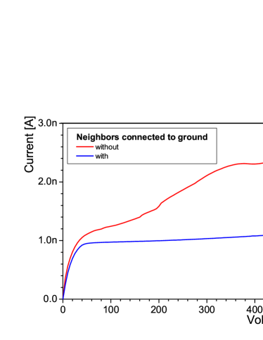
The leakage current of a single pad as a function of the bias voltage is shown in Figure 17a. Putting the neighbouring pads on ground stabilises the measurement and reduces the current values by a factor of two. The leakage currents of all the pads of one sensor have been measured at a bias voltage of 500 V. All pads except one have a leakage current in the range from 1 to 4 nA. Less than 5% of all pads have a break-through voltage below 500 V. For other sensors the results are similar.
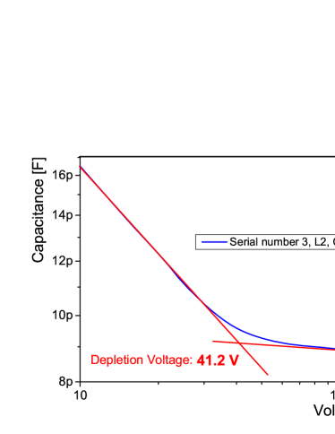
The capacitance as a function of the bias voltage for a pad is shown in Figure 17b. Also shown is how the value of the full depletion voltage is obtained. Values from 39 V to 43 V were found. At a voltage of 100 V the pad capacitance values are between 8 pF for the smallest pads and 25 pF for the largest pads.
6 ASIC developments
Since the occupancy in BeamCal and LumiCal is relatively large they must be read-out after each bunch crossing. Therefore special front-end and ADC ASICs have been developed which match the timing of the ILC – bunch trains with a frequency of 5 Hz and about one ms duration with 300 ns between bunches. Since the ASICs are positioned at the outer radius of the calorimeters the expected radiation dose is noncritical. From Monte Carlo simulations less than 140 Gy and about one Gy are estimated for BeamCal and LumiCal, respectively, for one year of operation at 500 GeV centre-of-mass energy and nominal beam parameters.
6.1 LumiCal readout
The design of the LumiCal front-end electronics was performed for the proposed detector architecture [40]. The front-end ASIC is supposed to work in two modes, the physics mode and the calibration mode. In the physics mode, electromagnetic showers will be measured with large energy depositions on the pads. The front-end ASIC must process signals up to at least 6 pC per channel. In the calibration mode, MIP signals from single relativistic muons will be measured. The minimum size of these signals is 2 fC, corresponding to the low end of the Landau distribution for MIPs in 300 m thick silicon. From the sensor segmentation a range of pad capacitances between 10 pF and 100 pF was obtained333The sensor segmentation was revised later, resulting in pad capacitances between 10 pF and 25 pF.. Because of the high expected occupancy, the front-end ASIC needs to be fast enough to resolve signals from subsequent bunch crossings which are separated in time by about 300 ns.
The simulations of LumiCal indicate that the shower reconstruction needs at least 8 bit precision. Severe requirements set on the readout electronics power dissipation may be strongly relaxed if switching of the power between bunch trains is done. This is feasible since in the ILC experiments after each 1 ms bunch train there will be a pause of about 200 ms [16].
6.1.1 Front-end electronics design
The chosen front-end architecture comprises a charge sensitive amplifier, a pole-zero cancellation circuit (PZC) and a shaper, as shown in Figure 19. In order to cope with large charges in the physics mode and small ones in the calibration mode a variable gain in both the charge amplifier and the shaper is applied. The mode switch in Figure 19 changes the effective values of the feedback circuit components , , , and therefore the transimpedance gain of the front-end ASIC is changed.

The low gain (large ) is used for the physics mode when the front-end processes signals from large charge depositions in the sensor, while the high gain (small ) is used in the calibration mode. Assuming high enough open loop gain of the pre-amplifier () and the shaper amplifier (), the transfer function of this circuit is given by
| (6) |
By setting properly the PZC parameters () and by equalising the shaping time constants (), one obtains the first order shaping, equivalent to a CR-RC filter, with a peaking time . A simple first order shaping is chosen as a trade-off between the noise and the power dissipation. Regarding the noise, the main requirement is to obtain in calibration mode the signal to noise ratio of about 10 for the largest sensor capacitances. Both of the amplifying stages () are designed as folded cascodes [41] with active loads, followed by source followers. In the prototype ASIC, eight front-end channels are implemented. A more detailed discussions of the front-end ASICs can be found in Ref. [42].
6.1.2 Front-end electronics measurements
Figure 20a shows the response of the front-end channel to charge injected through the input test capacitance for different values of the input capacitance, , within the interesting range. The sensor capacitance is simulated with an external capacitor.


It is seen that both the amplitude and the peaking time are not sensitive to the value of the input capacitance in agreement with HSPICE simulations.
The output noise has been measured using a HP3400 true r.m.s. meter [43]. The equivalent noise charge, ENC, as a function of input capacitance is shown in Figure 20b. Results obtained for the physics and calibration modes are shown on the same plot. Since the HP3400 bandwidth is only up to 10 MHz the numbers may be underestimated by about 20%. The measured ENC as a function of are in agreement with simulations. In particular, in the calibration mode the signal to noise ratio of 10 is maintained for input capacitances up to about 100 pF. For a few points additional noise measurements have been performed by measuring the output noise spectra using a HP4195A spectrum analyser [43] and then integrating it numerically. The results of such measurements are added in Figure 20b. They agree within their uncertainties with the HP3400 measurements.
In order to test the effectiveness of the PZC circuit, the front-end response has been measured as a function of the rate of input pulses. To avoid input charges of both polarities when using a square-wave test signal, the staircase test waveforms are synthesised using the Tektronix AWG2021 waveform generator. It was found that the change in amplitude reaches 2% for input rates of about 3 MHz and is quite insensitive to the input capacitance. The power consumption of about 8.9 mW/channel is measured in accordance with expectations from simulation.
6.1.3 ADC design
As a compromise between speed, area and power consumption the ADC was designed using pipeline technology. A 1.5-bit per stage architecture is chosen because of its simplicity and immunity to the offsets in the comparator and amplifier circuits. The prototype ADC consists of an input sample and hold circuit, 9 pipeline stages and digital correction circuitry. In addition, the power switching feature is also implemented. More details about the ADC design can be found in Ref. [44].
6.1.4 ADC performance measurements
The static measurements of the Integral Nonlinearity, INL, and the Differential Nonlinearity, DNL, obtained at a sampling frequency of 20 MHz, are shown in Figures 21a and 21b, respectively. These parameters are calculated using the histogramming method. The measured INL is always less than 1 LSB while the DNL is below 0.5 LSB.


These results attest to a very good ADC linearity. To estimate the dynamic performance, measurements with sinusoidal wave input are performed [45]. An example of a measured Fourier spectrum using a 1.8 MHz full scale (0 dB) input signal sampled at 20 MHz is shown in Figure 22a.


It is seen that the noise and harmonic components are small enough not to affect significantly the resolution. The signal to noise ratio, SNHR, is measured as a function of sampling frequency as shown in Figure 22b. An SNHR of about 58 dB is obtained in the frequency range up to almost 25 MHz.
6.2 BeamCal readout
The BeamCal ASIC, designed for 180 nm TSMC technology, will be able to handle 32 channels. The two modes of operation require a front-end circuit capable of a wide performance envelope: high slew rate for standard data taking, and low noise for calibration. In standard data taking the occupancy is high, and therefore all data from a full bunch train must be recorded, to be read out between bunch trains. Because of its reliability, density and redundancy, a digital memory array will be used to store the data from all collisions in each bunch train. This choice requires a sampling rate of 3.25 MHz per channel, which is achieved by 10-bits, successive approximation analog-to-digital converters [46]. The small size of this ADC architecture allows to use one converter per channel.
In this front-end ASIC, the dominant noise source is the charge sensitive amplifier series noise. Assuming 40 pF input capacitance, high occupancy and the 300 ns period, a careful design of noise filtering and baseline restoration is necessary[47].
In order to take advantage of all the time available for signal processing, the filter for calibration operation has been implemented using switched-capacitor, SC, circuits [48]. This technique allows to precisely define the circuit time constants depending on the input clock frequency and the ratio of two capacitors. Baseline restoration is achieved by means of a fast gated reset, followed by a slow reset-release technique to reduce the effect of a split doublet. The slow reset-release is implemented using SC circuits.
In standard data taking operation, an adequate noise power is effectively achieved by means of a slow reset-release technique, similar to that used in calibration operation. An explicit filter for standard data taking operation is unnecessary, as the amplifier bandwidth suffices for noise filtering purposes.
Figure 23 shows a simplified block diagram for a single channel. In standard data taking operation, since filtering is unnecessary, the integrator is bypassed to reduce power consumption.

For design purposes, the transistor-level noise analysis has been carried out using the technique [49], which takes noise coefficients directly from SPICE simulation results. As this is a gated front-end, the system-level noise analysis has been done using the weighting function approach.
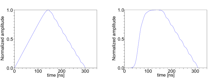
Since the system’s dominant noise source is series noise, a triangular-shaped weighting function effectively minimises the output noise power. The negative slope section of the triangular weighting function is easily implemented by means of an integrator – in this case, a SC integrator. The positive slope section is achieved by means of the slow reset-release technique mentioned earlier. The weighting function resulting from an ideal reset-release and a SC integrator is shown in Figure 24, left; a more realistic weighting function, reconstructed from SPICE simulation results, is shown in the right plot. In both cases, the target noise level is effectively achieved.
6.2.1 Circuit implementation
The charge sensitive amplifier is a folded-cascode amplifier with NMOS input device, connected to a switched-capacitor feedback network. The amplifier input transistor is biased at 450 A whereas the load works at about 50 A. The feedback network consist of two feedback capacitors of 0.9 pF and 44.1 pF for calibration and standard data taking modes, respectively. Both have a reset transistor, with a gate voltage driven by the switched-capacitor reset-release network. The amplifier output is pseudo-differential.
In order to isolate the amplifier from the filter’s SC-related kickback noise, a buffer circuit is used. The buffer also allows signal shifting, producing a more adequate common-mode level for the filter. The buffer consumes 130 A and consists of a source follower, with cascoded current source and an additional device to keep a nearly constant operational point in the input transistor. This serves the purpose of enhancing the buffer linearity.
The filter implemented is a fully-differential switched-capacitor integrator. Capacitor values were carefully designed in order to obtain the adequate noise performance. The core of the integrator is a class A/AB amplifier [50] that consumes 456 A.
The converter is a 10-bit, fully-differential successive approximation register ADC. The one included in the BeamCal ASIC has 16 fF unit capacitances, and similar versions with 4 fF and 2 fF unit capacitances were also designed for individual characterisation.
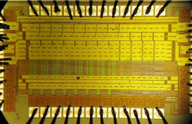
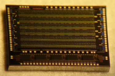
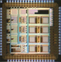
The BeamCal ASIC prototype, similar to the ASIC described in Figure 23, but including only three channels and no internal memory, was fabricated and is currently being tested. Figure 25 shows the 2.4 mm 2.4 mm die.
6.2.2 Test results
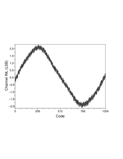
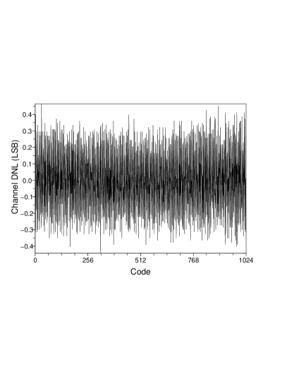
The ADC in the BeamCal ASIC has been quantitatively characterised, along with the additional versions of the ADC using smaller unit capacitances. Figures 26a and 26b show the INL and DNL for the ADC using 2 fF capacitors. The measurements were done at the nominal sampling frequency of 3.125MHz. The ADC input was a ramp, generated by 16-bit DAC, and the static performance measurements were calculated using the histogram method on the ADC digital output. The results are consistent with unit capacitance matching better than 0.1%. The INL cubic-like shape in Figure 26a is explained due to copper dishing effects, and will be corrected in future versions by re-arranging the capacitor array connections.
6.3 Pair monitor readout
A prototype ASIC has been designed with 36 readout cells arranged as an array of 66, as shown in Figure 27. Each cell has an amplifier block, comparator, an 8-bit counter and a 16 count-registers. The amplifier block consists of a charge sensitive pre-amplifier, a threshold block and a differential-amplifier. The pre-amplifier is a constant-current feedback-type amplifier. The time-over-threshold of the output signal is proportional to the injected charge through the constant current feedback in the pre-amplifier. In the 8-bit counter, the Gray code is used to count the number of hits. The 16 count-registers are prepared to store hit counts in one bunch train subdivided in 16 time slices. There are also decoders which select a count-register to store and readout the hit count. A shift register to select a readout pixel, data transfer to the output line and distributor of the operation signals are arranged around the 36 readout cells as a glue logic. The bonding pad is prepared in each cell to be attached to a sensor with bump bonding. The prototype ASIC has been produced with TSMC 250 nm CMOS process. The chip size is 44 mm2, and the readout cell size is 400400 m2.

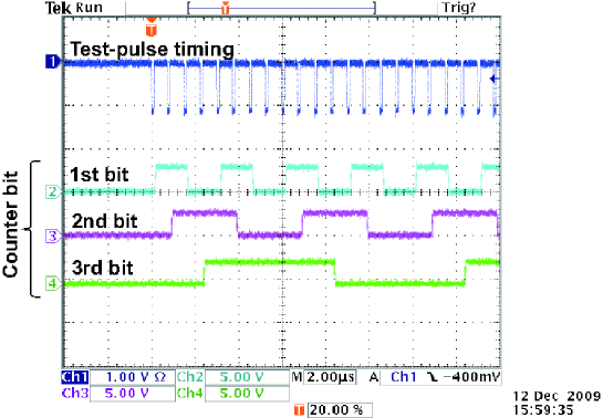
Figure 28 shows the response of the counter block. The state of the counter bits changes at each test pulse indicating a bunch crossing. The number of hits is measured in 16 time slices of a bunch train. The data stored will then be read-out during the inter-train time. The test is performed counting the hits in each time slice with a count rate of 4 MHz, larger than expected at the ILC. The number of hits was counted without any bit lost.
We also studied the noise level in the circuit. The count efficiency was investigated as a function of the threshold voltage at the comparator. Fitting the efficiency curve with the error function, a standard deviation of 0.94 mV was obtained. With the gain of mV per electron, this corresponds to an ENC of about 600 electrons.
As the next step, a pair-monitor prototype will be built in Silicon On Insulator technology. The sensor and readout ASIC will be prepared on the same wafer. This prototype will be used to investigate not only the standard characteristics but also the radiation tolerance. Currently, an ASIC is developed in OKI 0.2 m FD-SOI CMOS [51] technology.
7 Summary
A design for the instrumentation of the very forward region of a detector at the International Linear collider is presented. Two calorimeter are planned, LumiCal to measure precisely the luminosity and BeamCal, supplemented by a pair monitor, for a fast luminosity estimate and beam tuning. Both calorimeters extend the coverage of the detector to small polar angles. Parameters relevant for the physics program have been estimated by Monte Carlo simulations and found to match the requirements for the chosen geometry. Prototypes of the major components such as sensors, front-end ASICs and ADC ASICs are developed, produced and tested. Their measured performance fulfils the specifications derived from the Monte Carlo simulations. The results presented here demonstrate that the sensors and the ASICs are ready to be integrated into a fully functional prototype detector and to perform, as the next step, tests of fully assembled sensor plane prototypes.
8 Acknowledgments
This work is supported by the Commission of the European Communities under the 6th Framework Program "Structuring the European Research Area", contract number RII3-026126. Tsukuba University is supported in part by the Creative Scientific Research Grant No. 18GS0202 of the Japan Society for Promotion of Science. The AGH-UST is supported by the Polish Ministry of Science and Higher Education under contract Nr. 372/6.PRUE/2007/7. The INP PAN is supported by the Polish Ministry of Science and Higher Education under contract Nr. 141/6.PR UE/2007/7. IFIN-HH is supported by the Romanian Ministry of Education, Research and Innovation through the Authority CNCSIS under contract IDEI-253/2007. The VINCA group is benefiting from the project "Physics and Detector RD in HEP Experiments" supported by the Ministry of Science of the Republic of Serbia. J. Aguilar, P. Ambalathankandy and O. Novgorodova are supported by the 7th Framework Programme "Marie Curie ITN", grant agreement number 214560.
References
- [1] International Linearcollider Reference Report (2007) http://www.linearcollider.org/about/Publications/Reference-Design-Report.
- [2] The Compact Linear Collider Study, http://clic-study.web.cern.ch/clic-study/.
- [3] T. Abe et al., The International Large Detector: Letter of Intent, FERMILAB-LOI-2010-01, FERMILAB-PUB-09-682-E, DESY-2009-87, KEK-REPORT-2009-6, arXiv:1006.3396 (2010).
- [4] E. L. Berger et al., SiD Letter of Intent (2009) https://confluence.slac.stanford.edu/display/SiD/home.
- [5] H. Abramowicz et al., Instrumentation of the very forward region of a linear collider detector, IEEE Trans.Nucl.Sci. 51 (2004) 2983.
- [6] K. Mönig, Physics needs for the forward region, V. Workshop: Instrumentation of the Forward Region of a Linear Collider Detector, August, 26–28 (2004) DESY, Zeuthen, Germany, http://www-zeuthen.desy.de/lcdet/Aug_04_WS/aug_04_ws.html.
- [7] Ch. Grah and A. Sapronov, Beam parameter determination using beamstrahlung photons and incoherent pairs, \jinst32008P10004.
- [8] R. Bonciani and A. Ferroglia, Bhabha Scattering at NNLO, Nucl.Phys.Proc.Suppl.181-182 (2008) 259, T. Becher and K. Melnikov, JHEP 0706:084 (2007), S. Actis, M. Czakon, J. Gluza and T. Riemann, Fermionic NNLO contributions to Bhabha scattering, Acta Phys.Polon. B38 (2007) 3517, A.A. Penin, Two-loop photonic corrections to massive Bhabha scattering, Nucl. Phys. B 734 (2006) 185, M. Czakon, J. Gluza and T. Riemann, The Planar four-point master integrals for massive two-loop Bhabha scattering, Nucl. Phys. B751 (2006) 1.
- [9] S. Jadach, W. Placzek and B.F.L. Ward, BHWIDE 1.00: O(alpha) YFS exponentiated Monte Carlo for Bhabha scattering at wide angles for LEP1/SLC and LEP2, Phys. Lett. B 390 (1997) 298-308.
- [10] S. Agostinelli et al., Geant4- a simulation toolkit, Nucl. Inst. and Meth. A 506 (2003) 250-303.
- [11] MOKKA, A simulation program for linear collider detectors, http://polzope.in2p3.fr:8081/MOKKA/.
- [12] T.C. Awes, F.E. Obenshain, F. Plasil, S. Saini, S.P. Sorensen and G.R. Young, A simple method of shower localization and identification in laterally segmented calorimeters, Nucl. Inst. Meth. A 311 (1992) 130.
- [13] I. Sadeh, Luminosity measurement at the International Linear Collider, arXiv:1010.5992 (2010).
- [14] H. Abramowicz et al., Redefinition of the geometry of the luminosity calorimeter, EUDET-Memo-2008-09 (2008), http://www.eudet.org.
- [15] H. Abramowicz et al., Revised requirements on the readout of the luminosity calorimeter. EUDET-Memo-2008-08 (2008) http://www.eudet.org.
- [16] J. Brau et al., ILC Reference Design Report (2007) http://arxiv.org/abs/0712.1950.
- [17] D. Schulte, Beam-beam simulations with guinea-pig, CERN-PS-99-014LPCLIC-Note 387 (1998).
- [18] A. Seryi, T. Maruyama and B. Parker, IR optimization and anti-DID, SLAC-PUB-11662 (2006).
- [19] P. Bambade, V. Drugakov and W. Lohmann, The impact of Beamcal performance at different ILC beam parameters and crossing angles on stau searches, Pramana J. Phys. 69 (2007) 1123.
- [20] A. Heikkinen and N. Stepanov, Bertini Intra-nuclear Cascade implementation in Geant4, Proceedings of CHEP03, nucl-th0306008 (2003) La Jolla, California.
- [21] C. Coca et al., Expected electromagnetic and neutron doses for the BeamCal at ILD Rom. J.Phys 55 (2010) 687.
- [22] T. Tauchi and K. Yokoya, Nanometer beam-size measurement during collisions at linear colliders, Phys.Rev.E 51 (1995) 6119-6126.
- [23] T. Tauchi, K. Yokoya and P. Chen, Pair creation from beam-beam interaction in linear colliders, Part. Accel. 41 (1993) 29-39.
- [24] K.Ito, Study of Beam Profile Measurement at Interaction Point in International Linear Collider, arXive: 0901.4151 (2009).
- [25] A. Elagin, The optimized sensor segmentation for the very forward calorimeter, in proceedings of the 2005 International Linear Collider Physics and Detector Workshop, ECONF C0508141:ALCPG0719 (2005) Snowmass, Colorado.
- [26] J. Blocki et al., LumiCal new mechanical structure, EUDET-Memo-2009-10 (2009) http://www.eudet.org/.
- [27] J. Blocki et al., Laser alignment system for LumiCal, EUDET-Report-2008-05 (2008) http://www.eudet.org.
- [28] C. Rimbault, P. Bambade, K. Monig and D. Schulte, Impact of beam-beam effects on precision luminosity measurements at the ILC, \jinst22007P09001.
- [29] W. Kilian, WHIZARD: A generic Monte-Carlo integration and event generation package for multi-particle processes, LC-TOOL-2001-039 (2001).
- [30] V. N. Pozdnyakov, Two-photon interactions at LEP, Phys. Part. Nucl. Lett. 4 (2007) 289-303.
- [31] S. Jadach, E. Richter-Was, B.F.L. Ward and Z. Was, Monte Carlo program BHLUMI for Bhabha scattering at low polar angle with Yennie-Frautschi-Suura exponentiation, Comp. Phys. Commun. 70 (1992) 305-344.
- [32] B. Pawlik et al., BARBIE V4.3, Simulation-package of the LumiCal Detector, http://www.ifj.edu.pl/dept/no1/nz13/barbi.php.
- [33] I. Smiljanic et al., TOWARDS A FINAL SELECTION FOR LUMINOSITY MEASUREMENT, Proceedings of the Workshop of the Collaboration on Forward Calorimetry at ILC (2008), Belgrade Serbia.
- [34] Ch. Grah et al., Report to the Detector R&D Panel– Instrumentation of the Very Forward Region, http://www.desy.de/prc/docs_rd/prc_rd_02_01_update_05_07.pdf (2007) Hamburg, Germany.
- [35] S. Boogert et al., Polarimeters and Energy Spectrometers for the ILC Beam Delivery System, \jinst42009P10015.
- [36] S-DALINAC: Superconducting DArmstadt LInear ACcelerator, http://www.ikp.tu-darmstadt.de/beschleuniger_1/S-DALINAC.de.jsp.
- [37] Ch. Grah et al., Radiation hard sensor for the BeamCal of the ILD detector, Proceedings of the IEEE conference, October 27 – November 3 (2007) Honolulu, USA.
- [38] Ch. Grah et al., Polycrystalline CVD Diamonds for the Beam Calorimeter of the ILC, IEEE Trans.Nucl.Sci. 56 (2009) 462.
- [39] J. Blocki et al., Silicon Sensors Prototype for LumiCal Calorimeter, EUDET-Memo-2009-07 (2009). http://www.eudet.org.
- [40] M. Idzik et al., Status of VFCAL, EUDET-memo-2008-01 (2008). http://www.eudet.org.
- [41] E. Beuville et al.. AMPLEX, a low-noise, low-power analog CMOS signal processor for multi-element silicon particle detectors, Nucl. Instr. and Meth., A288a (1990) 157-167.
- [42] M. Idzik, Sz. Kulis and D. Przyborowski, Development of front-end electronics for the luminosity detector at ILC, Nucl. Instr. and Meth., A 608 (2009) 169-174.
- [43] http://www.home.agilent.com.
- [44] M. Idzik, K. Swientek and Sz. Kulis, Development of a Pipeline ADC for the Luminosity Detector at ILC, \jinst52010P04006.
- [45] IEEE standard for terminology and test methods for analog-to-digital converters, IEEE-STD-1241 (2000).
- [46] J.L. McCreary and P.R. Gray, All-MOS charge redistribution analog-to-digital conversion techniques. I. Solid-State Circuits, IEEE Journal of, 10(6) (1975) 371–379.
- [47] H. Spieler, Semiconductor Detector Systems. Oxford University Press (2005) Oxford, UK.
- [48] R. Gregorian, K.W. Martin, and G.C. Temes, Switched-capacitor circuit design, Proceedings of the IEEE, 71(8), (1983),941–966.
- [49] F. Silveira, D. Flandre, and P.G.A. Jespers, A based methodology for the design of CMOS analog circuits and its application to the synthesis of a silicon-on-insulator micropower OTA. Solid-State Circuits, IEEE Journal of, 31(9) (1996) 1314–1319.
- [50] S. Rabii, Design of Low-Voltage Low-Power Sigma-Delta Modulators, PhD thesis, Stanford University, (1998).
- [51] Y. Arai, Electronics and sensor study with the OKI SOI process, in proceedings of the Topical workshop on electronics for particle physics (TWEPP-07), September 3–7 (2007) Prague, Czech Republic.