Computational Modalities of Belousov-Zhabotinsky Encapsulated Vesicles
Abstract
We present both simulated and partial empirical evidence for the computational utility of many connected vesicle analogs of an encapsulated non-linear chemical processing medium. By connecting small vesicles containing a solution of sub-excitable Belousov-Zhabotinsky (BZ) reaction, sustained and propagating wave fragments are modulated by both spatial geometry, network connectivity and their interaction with other waves. The processing ability is demonstrated through the creation of simple Boolean logic gates and then by the combination of those gates to create more complex circuits.
Keywords: Belousov-Zhabotinsky reaction, computation, logic gates, half adder, excitable media, unconventional computing
1 Introduction
The last half of the twentieth century has been witness to huge leaps in technology spanning all areas of science. One of the most noticeable areas has been the dramatic success of the vonn Neumann [41] architecture electronic digital computer. Although modern digital computers or the software has not advanced to a point where one computer could independently create another technologically superior computer, or where software could compose more advanced software111A so called point of singularity., one could argue that from a purely technological perspective such a point has already been passed. It is has now become extremely difficult to design future computers (and develop their software) without the aid of existing computers (and software development tools). In spite of such advances the current computer architecture will always struggle with certain problems.222For example problems known to be NP hard, where the scale of the problem is known, the solution easily tested, but a solution remains intractable with current algorithms. Attempting to advance computing beyond the current dogma, lays the field of ‘Unconventional Computing’ [6]. This is an area of study that explores alternative computational representation, substrates and strategies, the results of which not only create novel experimental processing devices [1], but also contribute towards algorithms operating on conventional serial digital computers. One direction in this genre is the study of reaction diffusion (RD) computing [4]. Where the innate behaviour of a chemical reaction and subsequent diffusion in space and time can be used to present and manipulate information. A suitable and convenient chemical reaction for such processing is the Belousov-Zhabotinsky (BZ) reaction, a type of reaction that is subject to non-equilibrium thermodynamics creating a nonlinear chemical oscillator [44]. In certain formulations the BZ reaction can produce visible travelling waves which can be used to represent information [43]. Wave development is effected not only by the reaction conditions, but by geometric obstacles and collisions with other waves. Computation circuits analogous to electronic circuits can be created with chemical pathways (conductors) routed through a passive substrate (insulator) with waves representative of signals (electron flow).
In order to illustrate the possibility of computation in a BZ substrate some of the key components that are used to create electronic digital computers have been created, such as; diodes [10, 15, 22], coincidence detector [19] and logic gates [38, 35, 26, 18]. These components have been combined to create more complex circuits such as memory [27, 17, 16], counters [19] and binary adders [9]. These circuits serve to demonstrate that it is possible to create computational devices by modelling existing digital components and functions within the RD frame work, this approach amounts to conventional computing on an unconventional substrate. More interesting are some systems that exemplify unconventional processing and media, such as robot control [7, 2] shortest path calculation [36, 32, 33, 11, 3], image processing [24, 8], information encoding [13] and direction detection [28].
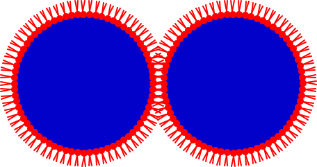
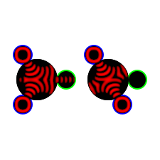
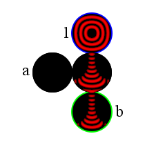
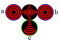
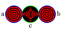
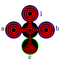
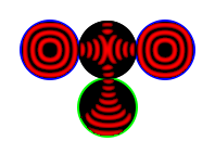
Contrary to these previous computation approaches in a BZ medium we have focused on exploring the utility of connecting small spherical processing elements containing BZ medium (vesicles) into functional networks [29]. Vesicles can be created by surrounding a solution of BZ reactant with a mono-layer of lipids [34]. This cell like structure has some interesting parallels with real neurons. When two or more vesicles are pressed together in solution the gap between the lipid layer forms a chemical junction similar to a synaptic cleft. Transmission of excitation from one vesicle to another could be possible and the effectiveness modulated by the suspension solution. Furthermore the oscillatory nature of the BZ reaction can be likened to the up-state firing (excitation) and down-state (inhibition) of neural activity. Travelling waves can be created when the BZ solution is in a sub excitable mode and waves can used to represent information signals, analogous to electrical spike trains in neurons. Connections between vesicles could be arranged in such a way as to create functional nuclei (Fig. 1). Reaction transmission in mono-layer lipid coated droplets (2D vesicles) of oscillating BZ solution has recently been reported [37].

In terms of connection, self adaptation and longevity the vesicleneuron analogy does not hold. Real neurons are typified by their distributed connectedness, ability to learn and self sustain. Vesicles under consideration in this work are only connected locally, also they cannot be sustained beyond exhaustion of the reagent and at this point no adaptation mechanism has been devised. Nevertheless the rich phenomenological behaviour of the BZ reaction connected in complex networks could give rise to functions and insight to the sort of processing achieved by biological circuits.
The remainder of the paper is comprised of the following: Section 2.1 details the method of BZ numerical computer simulation and graphical presentation. Section 2.2 introduces vesicle simplification, geometry and networking. Simulation results exploring the vesicle geometry, connectivity and membrane function are presented in section 2.3. Elementary logic gates are presented in section 3.1 and more complex circuits are presented in section 3.2 & 3.3. The results are discussed, future directions considered and a summary presented in the remaining sections 4, 5 & 6.
2 Methods
2.1 Computer simulations
We have employed a two variable version of the Oregonator model [30] as a model of the BZ reaction [43, 44] adapted for photo-sensitive modulation of the \cfRu-catalysed reaction [23].
Variables and are the local instantaneous dimensionless concentrations of the bromous acid autocatalyst activator \cfHBrO2 and the oxidised form of the catalyst inhibitor \cfRu(bpy)3^3+. symbolises the rate of bromide production proportional to applied light intensity. Bromide \cfBr^- is an inhibitor of the \cfRu-catalysed reaction, therefore excitation can be modulated by light intensity; high intensity light inhibits the reaction. Dependant on the rate constant and reagent concentration represents the ratio of the time scales of the two variables and . is a scaling factor dependent on the reaction rates alone. The diffusion coefficients and of and were set to unity and zero respectively. The coefficient is set to zero because it is assumed that the diffusion of the catalyst is limited.
| Parameter | Value | Description |
|---|---|---|
| Ratio of time scale for variables and | ||
| Propagation scaling factor | ||
| Stoichiometric coefficient | ||
| Excitability level (proportional to light level) | ||
| Activator \cfHBrO2 | ||
| Inhibitor \cfRu(bpy)3^3+ | ||
| Activator diffusion coefficient | ||
| Inhibitor diffusion coefficient | ||
| Spatial step | ||
| Time step |
Numerical simulations were achieved by integrating the equations using the Euler-ADI333Alternating direction implicit method. method [31] with a time step and a spatial step . Experimental parameters are given in Tab. 1.
Networks of discs where created by mapping 2 different values (proportional to light intensity) onto a rectangle of homogeneous simulation substrate. To improve simulation performance the rectangle size was automatically adapted depending on the size of the network, but the simulation point density remained constant throughout. The excitation levels, relate to the partially active disc interiors and non-active substrate.
Discs are always separated by a single simulation point wide boundary layer. Connection apertures between discs are created by superimposing another small link disc at the point of connection (typically a 2 6 simulation point radius), simulation points have a 1:1 mapping with on screen pixels. The reagent concentrations are represented by a red and blue colour mapping; the activator, is proportional to red level and inhibitor, proportional to blue. The colour graduation is automatically calibrated to minimum and maximum levels of concentration over the simulation matrix. The background illumination is mono-chromatically calibrated in the same fashion proportional to , white areas are inhibitory and dark areas excited.
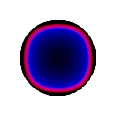
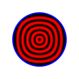
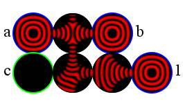
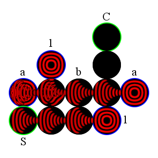
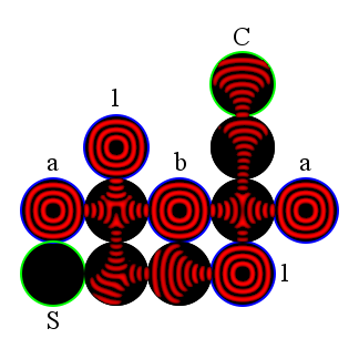
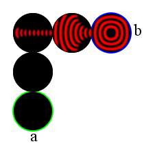
Wave fragment flow is represented by a series of superimposed time lapse images (unless stated otherwise), the time lapse is 50 simulation steps. To improve clarity, only the activator () wave front progression is recorded. Figure 2 illustrates the same wave fragment in both colour map ( & ) and time lapse versions ().


Inputs are created by perturbing a small circular area of the activator () set to a value of 1 with a radius of 2 simulation points in the center of the disc. All discs representing inputs and outputs are highlighted with a blue and green border respectively.
2.2 Vesicle geometry, connectivity and networking
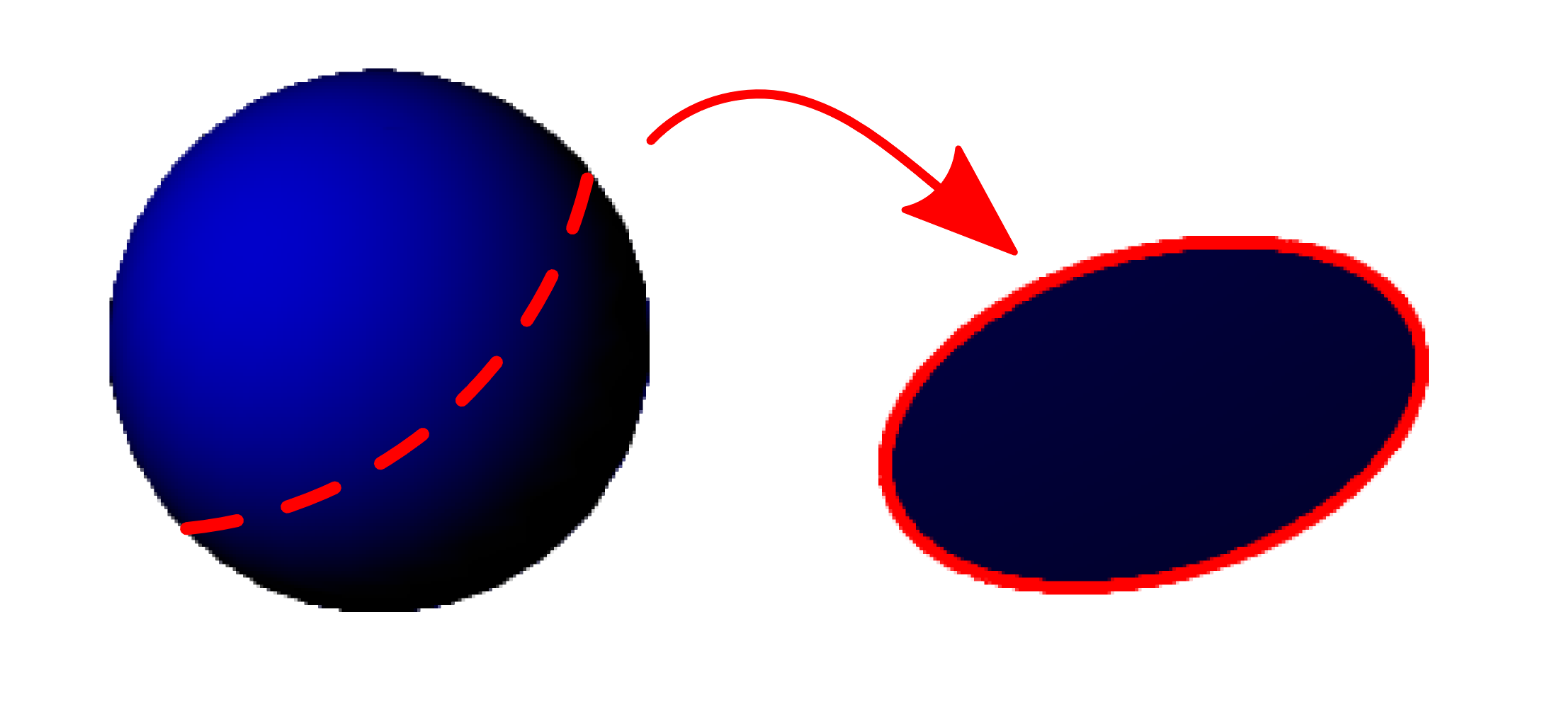
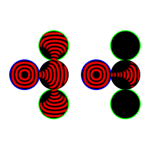
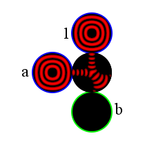
The three dimensional (3D) vesicle connection opportunities and complex internal wave reactions represent a rich computation substrate. Such depth raises difficulties when attempting to manually explore computation modalities. To reduce the complexity to a level where manual design is tractable the vesicles in this study have been approximated into two dimensional (2D) vesicles (discs). A disc is created by extracting an imaginary central slice, a cross section of a BZ vesicle (Fig. 3). This reduction also permits the opportunity of easily reproducing simulations by projecting circuits onto a 2D photo sensitive BZ gel. Signals are discrete, wave fragments represent the presence or absence of a particular signal.
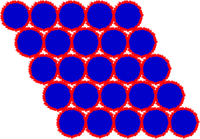
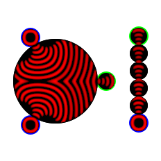
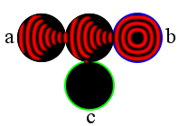
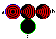
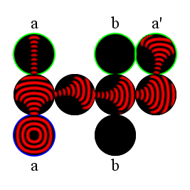
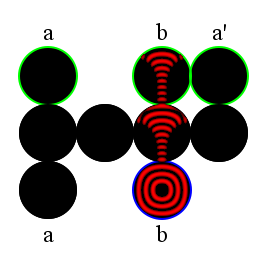
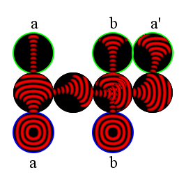
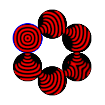
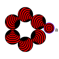
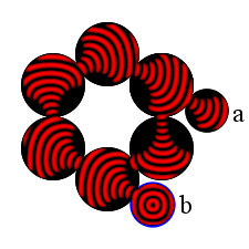
In a previous study we have shown that logic circuits can be created with uniform discs arranged in hexagonal networks [9], hexagonal packing being the most efficient method of sphere (disc) packing. Further opportunities to modulate wave fragment behaviour are presented when disc size, connection angle and connection efficacy are combined in non-homogeneous networks. Disc size can be adjusted to permit or restrict internal wave interactions, producing either larger reaction vessel discs or smaller communications discs (Fig. 4a). Connection angle between discs can be used to direct wave collisions (Fig. 4b) and connection efficiency can effect the wave focus (Fig. 4c).
2.3 Computer simulation experiments
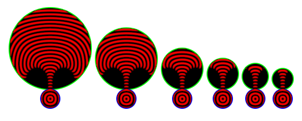
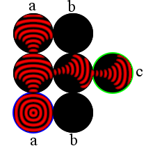
Increasing the relative disk size can be used not only to allow space for wave fragment collisions (Fig. 4a) but other effects are also apparent. Figure 5 illustrates the front development of the same wave through progressively smaller terminating discs. In the larger discs the wave fragment has more space in which to develop and spreads out to the majority of the disc perimeter, conversely in the smaller discs the wave fragment doesn’t have time to develop and terminates almost directly opposite the entry aperture.
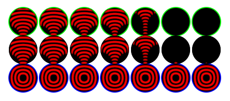
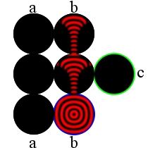
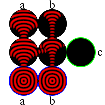
Wave fragments cannot survive when the fragment mass drops below some critical level [25] and this is evident when comparing progressively smaller aperture sizes with fixed size discs. In our system and with a disc radius of 28 units444Simulation grid points. the critical level surrounds an aperture gap of 4 units. Below that fragments do propagate through the aperture but quickly die. The narrow beam produced as a result of a 4 unit aperture (type J1) presents an opportunity to deflect the wave to alternate exits and perform ballistic style computation [14]. We have found that using a narrow beam aperture in orthogonal networks where wave fragments do not normally propagate into connected perpendicular discs particularly useful in creating simple logic gates (Sect. 3.1). Furthermore, diode junctions can be created when networks of narrow (type J1) and broadband (type J2) are combined (Sect.3.2). Although more functionality could be achieved with more subtle aperture adjustments [5] further explorations in this work rely on combining just the two types, narrow (J1) and broadband (J2) (Fig. 4c).
3 Results
3.1 Elementary logic gates
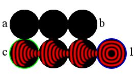
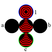
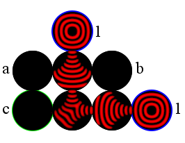
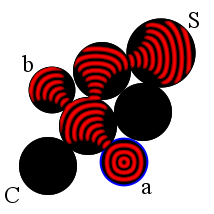
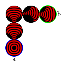
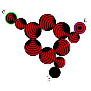
Electronic logical gates form the building blocks of more complex digital circuitry forming the foundations of complex high level components such as microprocessors. Although we do not envisage creating traditional vonn Neumann architecture microprocessors in BZ vesicles, the ability to create simple logic gates with BZ vesicles demonstrates that (like electronics) the medium and architecture is capable of such processing. Logic gates and composite circuits of logic gates have been created several times before using the BZ substrate, for example [38, 35, 26, 18]. Here we illustrate a selection of key gates can be created using nothing other than interconnected BZ discs. Figure 7 illustrates the operation of the most elementary of gates the inverter (NOT gate). The circuit operation starts with the simultaneous application of the circuit input (left most disc) in conjunction with the source (permanent logical ‘1’) input (top most disc). The circuit operation terminates by observing the output disc (lower most disc) at a time when either result state would be present. If the progression of a wave fragment through a disc is considered as 1 step then the output disc will hold a valid result after 2 steps from the application of the source input. Incorporating a parallel un-modulated source signal that travels from output to input could also be used to indicate the point at which the output discs holds a valid output. In this case this would simply consist of 3 serial discs.
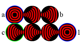
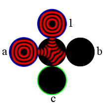
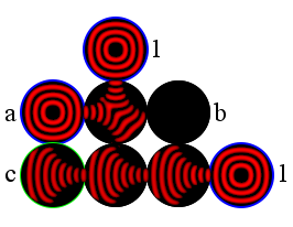
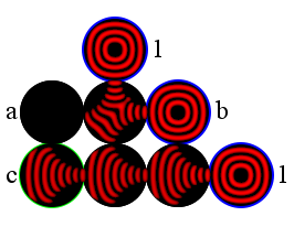
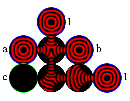
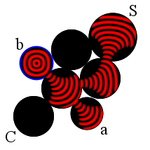
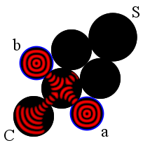
The operation of an AND gate and the inversion, the NAND gate are shown in Fig. 8 & Fig. 9. The result of a wave collision in the NOT gate was exploited to deflect and extinguish the source wave into the disc edge, whereas in the AND gate the collision between the two inputs results in 2 perpendicular fragments, one of which develops in the output cell to produce the result.
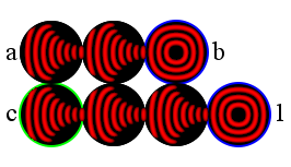
A NAND gate can created by combining the NOT gate and the AND gate Fig.9. NAND gates are known as universal gates since all other gates can be created from arrangements of NAND gates alone.555NOR gates are also universal gates. The NOT gate (Fig. 7) is integrated below the AND gate in the lower row (Fig. 8) where the activity of a horizontal source signal inverts the vertical output.
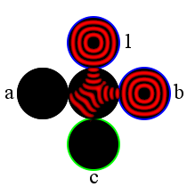
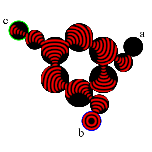
The OR gate is used to detect the presence of one or more signals. A logical ‘1’ on any input results in an output (Fig. 10). Common amongst all these gates, the output value of a logical ‘1’ or ‘0’ as indicated by the presence or absence of wave is only valid at a specific point in the development and in these instances, approximated to be proportional to time. For example the OR gate output is sampled after a wave fragment has travelled by one disc unit (). Therefore the annihilation of the ()() case and the continuation of the waves into opposing input cells for cases ()() and ()() does not effect the outcome.
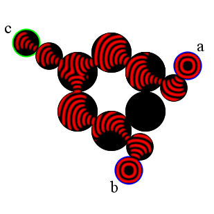
The XOR gate is used to signal a difference between signals, producing an output when inputs alternate regardless of the composition of the difference. Figure 12 illustrates the BZ disc implementation along with the inversion NXOR in Fig. 11.
3.2 Half adder
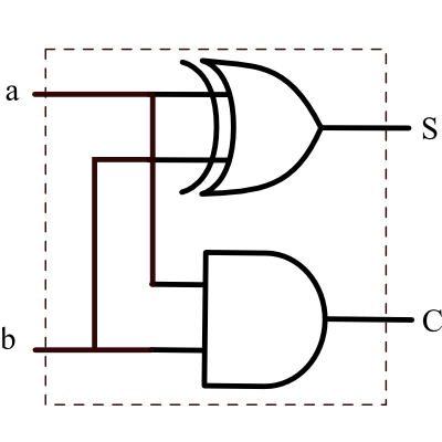
The half adder is a sub-system used in binary addition circuits. The half adder adds two binary digits and when connected with another half adder creates a full 1 bit adder. One bit adders can then in turn be connected together to make bit adders (Fig. 13). A half adder can be constructed from a combination of two logic gates the XOR and AND gate. There are two inputs ( & ) and two outputs ( & ), the binary sum () of & is achieved by the XOR gate () and inability of the configuration (overflow) to present the input is achieved with a carry () output, ().
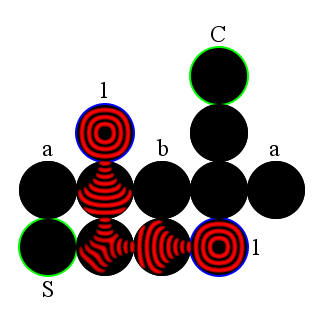

A 1 bit half adder created from BZ discs can also be constructed from connecting a BZ disc AND gate and XOR gate (Sect. 3.1). Figure 14 shows the BZ disc conjunction for the half adder circuit. The input needs to be repeated on the other side of input in order for this circuit to work. This is necessary in order to overcome the signal passing problem, a universal problem for systems where signals propagate along specific planular channels. There are two ways to overcome this problem, either add identity to the signals in such a way that signals can share the medium or share the medium at different times. How two or more waves could be identified and share the same space in this BZ system remains unclear because of the diffusive nature of the reaction. However sharing a channel medium in time666In communications systems this is known as Time Division Multiplexing (TDM). is possible if the time difference between signals is large enough to prevent the refractory tail from one extinguishing the other. Figure 15 illustrates one such temporal separation strategy, where signal passes over signal but becomes shifted in time. The circuit operates with two types of apertures, one that creates a narrow beam (type J1) wave and another that creates a broad beam (type J2) wave. Signals & travel from bottom to top, with on the left and on the right. The signal is split at the junction to the first disc and a fragment travels horizontally towards . Meanwhile is already traversing the first disc and has progressed into the final disc before crosses the path allowing to cross . A time shift now exists between and so any further processing between and must therefore delay by . This strategy relies on allowing sufficient time for the refractory tail of signal to have a negligible effect on . If the signals are not sufficiently separated then will extinguish which can in another context be used as another logical construction (Fig. 16).
Venturing into 3 dimensions (3D) resolves the signal passing problem all together, allowing signals to be routed vertically. At this stage only 2 dimensional (2D) structures of discs have been explored, but these are approximations of our target computation node, a 3D BZ vesicle. In this current 2D perspective, overcoming the signal passing problem via interconnecting linking layers above and below planular 2D functions seems the next logical step analogous to a methodology used in 2 layer and multilayer electronic circuit boards.
Another specific solution for the half adder circuit which removes the need to repeat one of the inputs is possible if all the signal modulation techniques are exploited; disc connection geometry, disc size and aperture efficacy (Sect. 2.2). Figure 17 demonstrates a half adder design where most of the processing occurs in one central reactor disc. The central disc achieves the AND function (Fig. 17c) and the XOR function (Fig. 17b & c). Considering the central disc principally in terms of an AND gate; then the XOR function can be considered as being derived from the AND gate response to input sets and . The outputs of which are curved around into an OR gate in the output disc creating the XOR function.
3.3 Memory cells
Memory is an essential facet of both adaptive behaviour in Nature and in synthetic computation. It permits animals and machines to build an internal state independent from the current external world state. In this section we present a simple 1 bit volatile read write memory cell constructed entirely with BZ discs. The cell design is independent but similar to previous designs [26, 27] in so much that the existence or absence of a rotating wave represents the setting or resetting of 1 bit of information.
When two BZ waves progress in opposite directions around an enclosed channel, loop or ring of connected discs, then at some point the two opposing wave fronts will meet and are always mutually annihilated (Fig. 19a). Nevertheless, if a unidirectional wave can be inserted into the loop then that wave front will rotate around the loop indefinitely777For as long as the chemical reagents can sustain the reaction. (Fig. 19b). Furthermore the rotating wave can be terminated by the injection of another asynchronous wave rotating in the opposite direction (Fig. 19.c). Opposing inputs into a loop are analogous to a memory set or reset. Reading the state of the cell without changing the state can be achieved by connecting another output node where a stream of pulses can be directed to modulate other circuits [20].
The loop and a unidirectional gate (diode) are the two key constructions of this type of memory cell. Unidirectional gates in BZ media have previously been created by exploiting asymmetric geometries or chemistry on either side of a barrier [10]. An alternative design is possible however using discs connected with different apertures. Figure 18 illustrates a diode constructed from a right angle junction connected by a broad band (type J2) aperture to a vertical column and by a narrow beam (type J1) aperture to a horizontal row. Signal flow is only possible from bottom to top () because of the asymmetric apertures in the right angle connecting the disc. The operation relies on the relationship between the wave expansion and the angle of the connection. Fine control of the wave beam would in theory allow other angles of connectivity [5] and other functions. In practice fine control of wave diffusion is however difficult to achieve and hence we have restricted our choice between just two types.
As the rotating wave progresses around the loop in the memory cell illustrated in Fig. 19, the opposing input cell also inadvertently becomes an output cell. This may be undesirable in some designs but can be easily resolved by adding another pair of diode junctions to the circuit. Figure 20 shows such a design, where opposing inputs are not affected by the opposing input.
4 Discussion
Our research is an exploratory component within a collaborative project that aims to create a lipid encapsulated BZ vesicle and organise those vesicles into a functional network. The lipid membrane and the non-linear oscillatory nature of the BZ medium encodes some of the features apparent in biological information processing. Whilst inter-neuron communication is electrical, modulation of that activity is chemical and in the case of individual neurons modulation dominates at the synaptic junction. The membrane between two vesicles can be considered a simple analog of the synaptic junction, a small contact area that can modulate signals in between vesicles. Similarly the electric upstate firing and downstate quiescence of neural signalling is an analog of chemical excitation and refraction. Connecting vesicles together presents the fascinating possibility of creating a chemical processing device similar in principle to biological systems. [29]
Another analog between Natural processing and vesicles is the relationship to artificial Life. The cell is the building block of all known life on Earth. Mechanistic explanation for the genesis of Life and the cell remain elusive, but a key aspect of cell morphology is the concept of a cell wall and the ability to separate one state (the outside) from another (the inside), the possibility for an increase in entropy [21]. One theory (amongst many) is a role for lipids in the spontaneous formation of simple cells and hence the development of a separate entity different from the surrounding environment. Whether spontaneous lipid cell formation played a role in early Life remains to be seen, but the principle of an enclosing membrane to a cell like unit appears essential in order separate environment from agent. Enclosing a nonlinear chemical oscillator such as the BZ reaction into a cell (vesicle) leads to another type of phenomena. If the reaction (upstate) in a vesicle can in some degree migrate across the membrane then the reaction in one vesicle could influence the reaction in another, and in turn be subject of influence. The nature of the excited and refractory temporal dynamics of the reaction can lead to interesting emergent ensemble behaviour [40]. Computer simulations of such behaviour of similar simple processing units, known as ‘Cellular Automata’ (CA) has been extensively studied [42] and can lead to interesting Life like behaviour [12].
The exploration in the computation modalities of BZ encapsulated vesicles is promising then on (at least) two levels. The macro scale of organised behaviour (classification of this work) and the small scale emergent oscillatory behaviour analogous to cellular automata. The parallel between the notion of a conscious single thread behaviour and the unconscious parallel emergent behaviour. In this study we have shown that most of the computation accomplishments of previous geometrically constrained BZ processing at the macro scale can be achieved with BZ discs alone. In extrapolating discs into spherical vesicles more interesting behaviour and processing is likely to be possible888The innate resolution of the signal passing problem (Sect.3.2) for example. albeit at the cost of the simplicity and clarity of design.
5 Future work
Experiments are currently in progress to replicate these simulation results in real chemistry (an example of the AND gate is shown in the appendix (Sect. 7)). Our goal is to explore computational modalities of interconnected discs and vesicles. In doing so we hope that such work will both inspire novel chemical computing and introduce new strategies for use in existing systems and other mediums (including silicon) or conventional computers. Implementing devices that are known to be an essential to perform conventional computation is useful for demonstrative purposes. Expunging the computing capabilities of geometrically modulated reaction diffusion computers. Nevertheless the innate massively parallel and deep temporal-spatial nature of such a substrate is a good candidate to explore the kind of computation problems for which vonn Neumann architecture machines perform so poorly. Previous studies have shown that RD systems are capable of performing computation in the conventional paradigm and this study has shown that distributing encapsulated RD units in cell like units is equally competent. On that basis other perhaps unknown structures and strategies could be developed beyond our current understanding. To achieve these aims and in part, not to be biased by known solutions and tradition design methodology our next step is to apply an evolutionary strategy to evolve functional networks of discs. We intend to focus on solving computational tasks for which the solutions are currently protracted in conventional systems.
6 Summary
Creating components, gates and circuits commonly used in the design of discrete conventional computers within geometrically constrained constructions containing sub-excitable BZ media has been extensively studied both in simulation and real chemistry. This work has shown that some of the previous circuits, logic gates, composite logic gate circuits (the half adder) and memory can be reproduced using networks of interconnected discs alone. Wave modulation through discs can be manipulated by changing the network interconnections, relative disc sizes and aperture efficiency. All the designs presented rely on a uniform excitability level of the reaction. This is an important consideration since discs or vesicles whose function relies on non-uniform excitation levels may eventually fail as reagents equalise across connecting junctions, additionally photo modulation of excitability is possible with discs in 2 dimensions, but otherwise impossible with vesicles in 3 dimensional structures. Elementary and universal logic gates and composite circuits have also been shown possible with a uniform disc size and aperture gap connected in a simple orthogonal network structure, whereas other circuits such as the diode and memory cell rely on a combination of different geometric connectivity, disc size and aperture efficacy.
7 Appendix
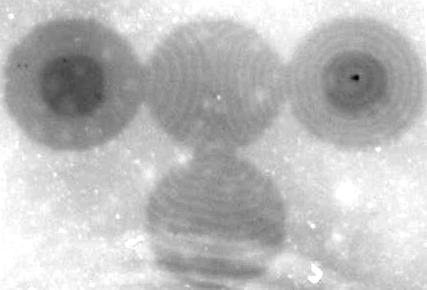
An example of some initial results from on-going laboratory work is shown in Fig. 21a. An identical background image generated from the simulation software, where light intensity is proportional to and is projected onto a thin layer of silica gel containing a photo sensitive (Ru(bpy)) catalyst for the BZ reaction. The gel is submerged in catalyst-free BZ reagents (NaBrO3, CH2(COOH)2, H2SO4 & BrMA).999Further details of chemistry and experimental apparatus are described in [39]. Waves are continuously initiated by inserting silver colloidal particles onto the gel surface at the center of the two input discs (dark centers, top left and right). Fine waves can be seen travelling out from each input disc, colliding in the central disc and then expanding into the output disk (bottom). For comparison the result of the simulated AND gate (Sect. 3.1) is shown in the adjacent frame (Fig. 21b). The real chemistry image (Fig. 21a) is a single image of multiple wave initiations, whereas the simulation image (Fig. 21b) is a composite of time lapse images of a single wave initiation.
8 Acknowledgements
The work is part of the European project 248992 funded under 7th FWP (Seventh Framework Programme) FET Proactive 3: Bio-Chemistry-Based Information Technology CHEM-IT (ICT-2009.8.3). The authors wish to acknowledge the support of the EPSRC grant number EP/E016839/1 for support of Ishrat Jahan. We would like to thank the project coordinator Peter Dittrich and project partners Jerzy Gorecki and Klaus-Peter Zauner for their inspirations and useful discussions [29].
References
- Adamatzky [2009] Adamatzky, A., 2009. From reaction-diffusion to physarum computing. Natural Computing 8 (3), 431–447.
- Adamatzky et al. [2004a] Adamatzky, A., Arena, P., Basile, A., Carmona-Galan, R., Costello, B., Fortuna, L. Frasca, M., Rodriguez-Vazquez, A., May 2004a. Reaction-diffusion navigation robot control: From chemical to VLSI analogic processors. IEEE Transactions on Circuits and Systems I: Regular Papers 51 (5), 926–938.
- Adamatzky and De Lacy Costello [2002] Adamatzky, A., De Lacy Costello, B., October 2002. Collision-free path planning in the Belousov-Zhabotinsky medium assisted by a cellular automaton. Naturwissenschaften 89 (10).
- Adamatzky et al. [2005] Adamatzky, A., De Lacy Costello, B., Asai, T., 2005. Reaction-Diffusion Computers. Elsevier Science Inc., New York, NY, USA.
- Adamatzky et al. [2010a] Adamatzky, A., De Lacy Costello, B., Bull, L., June 2010a. On polymorphic logical gates in sub-excitable chemical medium. http://arxiv.org/abs/1007.0034.
- Adamatzky et al. [2006] Adamatzky, A., De Lacy Costello, B., Bull, L., Stepney, S., Teuscher, C. (Eds.), 2006. Unconventional Computing 2007. Luniver Press.
- Adamatzky et al. [2004b] Adamatzky, A., De Lacy Costello, B., Melhuish, C., Ratcliffe, N., 2004b. Experimental implementation of mobile robot taxis with onboard Belousov-Zhabotinsky chemical medium. Materials Science and Engineering: C 24 (4), 541 – 548.
- Adamatzky et al. [2002] Adamatzky, A., De Lacy Costello, B., Ratcliffe, N. M., 2002. Experimental reaction-diffusion pre-processor for shape recognition. Physics Letters A 297 (5-6), 344 – 352.
- Adamatzky et al. [2010b] Adamatzky, A., Holley, J., Bull, L., De Lacy Costello, B., June 2010b. On computing in fine-grained compartmentalised Belousov-Zhabotinsky medium. http://arxiv.org/abs/1006.1900.
- Agladze et al. [1996] Agladze, K., Aliev, R. R., Yamaguchi, T., Yoshikawa, K., 1996. Chemical diode. Journal of Physical Chemistry 100 (33), 13895–13897.
- Agladze et al. [1997] Agladze, K., Magome, N., Aliev, R., Yamaguchi, T., Yoshikawa, K., 1997. Finding the optimal path with the aid of chemical wave. Physica D: Nonlinear Phenomena 106 (3-4), 247 – 254.
- Berlekamp et al. [1982] Berlekamp, E. R., Conway, J. H., Guy, R. L., 1982. Winning Ways for your Mathematical Plays. Vol. 2. Academic Press.
- Bollt and Dolnik [1997] Bollt, E. M., Dolnik, M., Jun 1997. Encoding information in chemical chaos by controlling symbolic dynamics. Phys. Rev. E 55 (6), 6404–6413.
- Fredkin and Toffoli [2002] Fredkin, E., Toffoli, T., 2002. Conservative logic, 47–81.
- Gorecka et al. [2007] Gorecka, J., Gorecki, J., Igarashi, Y., Feb 2007. One dimensional chemical signal diode constructed with two nonexcitable barriers. The Journal of Physical Chemistry 111 (5), 885–889.
- Gorecki and Gorecka [2005a] Gorecki, J., Gorecka, J., 2005a. Chemical programming in reaction-diffusion systems. In: Adamatzky, A., Teuscher, C. (Eds.), Unconventional Computing 2005: From Cellular Automata to Wetware. Luniver Press, pp. 1–12.
- Gorecki and Gorecka [2005b] Gorecki, J., Gorecka, J. N., 2005b. On mathematical description of information processing in chemical systems. In: T., A., Niezgodka, M. (Eds.), Mathematical approach to nonlinear phenomena; Modeling, analysis and simulations. Vol. 23 of GAKUTO International Series, Mathematical Sciences and Applications. pp. 73–90.
- Gorecki and Gorecka [2009] Gorecki, J., Gorecka, J. N., 2009. Computing in geometrical constrained excitable chemical systems. In: Meyers, R. A. (Ed.), Encyclopedia of Complexity and Systems Science. Springer-Verlag.
- Gorecki et al. [2009] Gorecki, J., Gorecka, J. N., Igarashi, Y., 2009. Information processing with structured excitable medium. Natural Computing: an international journal 8 (3), 473–492.
- Gorecki et al. [2003] Gorecki, J., Yoshikawa, K., Igarashi, Y., 2003. On chemical reactors that can count. Journal of Physical Chemistry 107 (10), 1664–1669.
- Harold [2001] Harold, F., 2001. The Way of the Cell. Oxford University Press, New York.
- Igarashia et al. [2008] Igarashia, Y., Jerzy Góreckia, b., Góreckac, J. N., 2008. One dimensional signal diodes constructed with excitable chemical system. Acta Physica Polonica B 39 (5), 1187–1197.
- Kuhnert [1986] Kuhnert, L., 1986. A new optical photochemical memory device in a light-sensitive chemical active medium. Nature 319, 393–394.
- Kuhnert et al. [1989] Kuhnert, L., Agladze, K. I., , Krinsky, V. I., January 1989. Image processing using light-sensitive chemical waves. Nature 337, 244–247.
- Kusumi et al. [1997] Kusumi, T., Yamaguchi, T., Aliev, R. R., Amemiya, T., Ohmori, T., Hashimoto, H., Yoshikawa, K., 1997. Numerical study on time delay for chemical wave transmission via an inactive gap. Chemical Physics Letters 271 (4-6), 355–360.
- Motoike and Yoshikawa [1999] Motoike, I., Yoshikawa, K., May 1999. Information operations with an excitable field. Phys. Rev. E 59 (5), 5354–5360.
- Motoike et al. [2001] Motoike, I. N., Yoshikawa, K., Iguchi, Y., Nakata, S., Feb 2001. Real-time memory on an excitable field. Phys. Rev. E 63 (3), 036220.
- Nagahara et al. [2008] Nagahara, H., Ichino, T., Yoshikawa, K., 2008. Direction detector on an excitable field: Field computation with coincidence detection. http://arxiv.org/pdf/nlin/0405063.
- NeuNeu [2010] NeuNeu, 2010. NeuNeu: Artificial wet neuronal networks from compartmentalised excitable chemical media project. http://neu-n.eu/.
- Noyes et al. [1972] Noyes, R. M., Field, R., Koros, E., Feb 1972. Oscillations in chemical systems. i. detailed mechanism in a system showing temporal oscillations. Journal of the American Chemical Society 94 (4), 1394–1395.
- Press et al. [1992] Press, W. H., Flannery, B. P., Teukolsky, S. A., Vetterling, W. T., Oct 1992. Numerical Recipes in C: The Art of Scientific Computing, 2nd Edition. Cambridge University Press, England.
- Rambidi and Yakovenchuck [1999] Rambidi, N. G., Yakovenchuck, D., 1999. Finding paths in a labyrinth based on reaction-diffusion media. Biosystems 51 (2), 67 – 72.
- Rambidi and Yakovenchuk [2001] Rambidi, N. G., Yakovenchuk, D., Jan 2001. Chemical reaction-diffusion implementation of finding the shortest paths in a labyrinth. Phys. Rev. E 63 (2), 026607.
- Stanley et al. [2010] Stanley, C. E., Elvira, K. S., Niu, X. Z., Gee, A. D., Ces, O., Edel, J. B., deMello, A. J., 2010. A microfluidic approach for high-throughput droplet interface bilayer (dib) formation. Chem. Commun. 46, 1620–1622.
- Steinbock et al. [1996] Steinbock, O., Kettunen, P., Showalter, K., 1996. Chemical wave logic gates. Journal of Chemistry Physics 100, 18970–18975.
- Steinbock et al. [1995] Steinbock, O., Toth, A., Showalter, K., 1995. Navigating complex labyrinths: Optimal paths from chemical waves. Science 267 (5199), 868–871.
- Szymanskia et al. [2010] Szymanskia, J., Igarashia, Y., Goreckia, J., Gorecka, J. N., 2010. Belousov-Zhabotinsky reaction in lipid covered droplets. (In press).
- Toth and K.Showalter [1995] Toth, A., K.Showalter, 1995. Logic gates in excitable media. Journal of Chemistry Physics 103, 2058–2066.
- Toth et al. [2009] Toth, R., Stone, C., Adamatzky, A., De Lacy Costello, B., Bull, L., 2009. Experimental validation of binary collisions between wave fragments in the photosensitive Belousov-Zhabotinsky reaction. Chaos, Solitons & Fractals 41 (4), 1605 – 1615.
- Vanag and Epstein [2001] Vanag, V. K., Epstein, I. R., Nov 2001. Pattern formation in a tunable medium: The Belousov-Zhabotinsky reaction in an aerosol OT microemulsion. Phys. Rev. Lett. 87 (22), 228301.
- von Neumann [2005] von Neumann, J., 2005. John von Neumann: Selected Letters. American Mathematical Society, London.
- Wolfram [2002] Wolfram, S., 2002. A New Kind of Science. Wolfram Media.
- Zaikin and Zhabotinsky [1970] Zaikin, A. N., Zhabotinsky, A. M., 1970. Concentration wave propagation in two-dimensional liquid-phase self-oscillating system. Nature 225 (5232), 535–537.
- Zhabotinsky and Zaikin [1973] Zhabotinsky, A. M., Zaikin, A. N., 1973. Autowave processes in a distributed chemical system. Journal of Theoretical Biology 40 (1), 45 – 61.