Dynamical bi-stability of single-molecule junctions: A combined experimental/theoretical study of PTCDA on Ag(111)
Abstract
The dynamics of a molecular junction consisting of a PTCDA molecule between the tip of a scanning tunneling microsope and a Ag(111) surface have been investigated experimentally and theoretically. Repeated switching of a PTCDA molecule between two conductance states is studied by low-temperature scanning tunneling microscopy for the first time, and is found to be dependent on the tip-substrate distance and the applied bias. Using a minimal model Hamiltonian approach combined with density-functional calculations, the switching is shown to be related to the scattering of electrons tunneling through the junction, which progressively excite the relevant chemical bond. Depending on the direction in which the molecule switches, different molecular orbitals are shown to dominate the transport and thus the vibrational heating process. This in turn can dramatically affect the switching rate, leading to non-monotonic behavior with respect to bias under certain conditions. In this work, rather than simply assuming a constant density of states as in previous works, it was modeled by Lorentzians. This allows for the successful description of this non-monotonic behavior of the switching rate, thus demonstrating the importance of modeling the density of states realistically.
I introduction
The scanning tunneling microscope (STM) is a valuable and versatile tool for the study and manipulation of nanoscale structures.binning ; moresco In scanning mode, it can be used to image surfaces with atomic resolution, and to probe the electronic density of states at a range of energy values. Alternatively, it can be brought into contact with surface features to form junctions and measure transport properties.Tao ; PTCDA_Kondo ; Pump1 ; Grill ; Lindsay ; Toher1 Nanostructures and devices can be manipulated and fabricated using an STM, with the possibility to pick up and deposit atoms and molecules using the tip.eigler ; eigler2 ; stroscio ; Lindsay An important aspect related to the tip-molecule interaction is the telegraph noise observed in the conductance in certain circumstances, which originates from the repeated switching of single atoms or functional groups between different stable configurations.stroscio ; PhysRevLett.86.672 ; stroscio2 ; Tao ; VioletaIancu09122006 ; werner ; PeterLiljeroth08312007 ; Kern Several physical mechanisms have been proposed to explain this phenomenon: thermal activation, vibrational heating (for intermediate biases)Gao ; ueba2004 ; ueba2005 ; ueba2009 ; domcke2004 and transition through an electronic excited state with no conformational bi-stability (for high biases).Elste If the masses involved are not too large (i.e. for a single atom), quantum tunneling is also possible.Lauhon
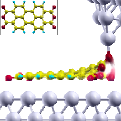
In this work, we present a systematic study of this switching behavior in the specific system of perylene-3,4,9,10-tetracarboxylic-dianhydride (PTCDA, inset in Fig. 1(a)) on Ag(111), using both experimental and theoretical methods. With results from density-functional (DFT) calculations and by extending a microscopic model developed in Ref. 22 to describe the coupling of an adsorbate energy level to the adsorbate vibrational excitations, a good agreement with the experimentally measured switching rates can be achieved.
PTCDA deposited on Ag(111) forms a highly ordered metal-organic interface, the electronic and geometric structure of which has been well-characterized using a variety of both experimental and theoretical techniques.Gloeckler ; tautz07 ; tautz07a ; Kraft The PTCDA molecules form long-range ordered commensurate monolayers on the Ag(111) substrate with two flat-lying chemisorbed molecules per unit cell in a herringbone arrangement (see Ref. 25). The chemisorption results in the former lowest unoccupied molecular orbital (LUMO) of the isolated molecule being shifted below the Fermi level of the silver surface, so that there is charge transfer from the substrate to the molecule thus producing a net negative charge on the molecule.Kraft
In previous experiments we have found that it is possible to form a chemical bond between the carboxylic oxygen atoms and the STM tip, if the latter is approached towards the molecule above one of the carboxylic oxygen atoms:PTCDA_Kondo ; Pump1 ; Toher1 the oxygen atom, followed by part of the carbon skeleton of the PTCDA molecule, jumps into contact with the tip. The most likely distance for this single switch to happen (without applying a bias voltage) is 6.65Å.PTCDA_Kondo In a theoretical analysis, carried out by calculating potential profiles of relaxed PTCDA molecules between tip and surface as a function of oxygen-surface separation for a range tip sample separations, we found the spontaneous jump into contact at 6.2Å,Toher1 in good agreement with experiment.
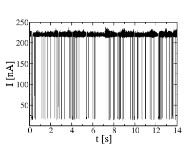
Once the molecular junction with the tip has been formed, there are two possible ways for the molecule to behave when the tip is retracted: either the molecule is peeled off from the surface completely or it falls back to the surface.PTCDA_Kondo We have further observed that, under certain conditions (see below), the current fluctuates in time between a high- and a low-conductance state, see e.g. Fig. 1(b) in which the telegraph noise in the current is evident. These two-state fluctuations can be explained by the switching of the molecule in and out of contact with the tip (see Fig. 1(a)). In the high-conductance state, one of the carboxylic oxygen atoms of the molecule forms a chemical bond with the tip (“up-state”), establishing a two-terminal molecular junction, while in the low-conductance state the molecule is bonded exclusively to the surface (“down-state”) so that a tunnel barrier is now present between the tip and the molecule. These switching processes of the molecule can also be seen in the topographic images taken with the tip very close to the surface.PTCDA_Kondo
II experimental methods
Our experiments have been performed with a CREATEC low temperature scanning tunneling microscope (5-6 K) in ultrahigh vacuum with a base pressure below 10-10mbar. The Ag(111) surface has been prepared by repeated sputtering/annealing cycles (Ar+ ion energy 0.8 keV, annealing at approximately 850 K). Surface quality has been controlled in situ with low-energy electron diffraction (LEED). The PTCDA molecules have been evaporated from a Knudsen cell at 580 K onto the surface at room temperature. An electrochemically etched tungsten wire has been used as the STM tip, which has been cleaned in situ by annealing. The final atomic sharpening has been done by the indentation of the tip into the clean metal substrate and/or by the application of voltage pulses. Tip quality has been checked by measuring the surface state of Ag(111). The PTCDA material (commercial purity 99%) has been purified by resublimation and outgassing in ultra high vacuum.
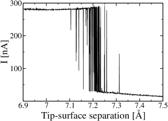
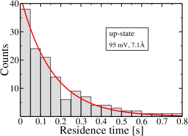
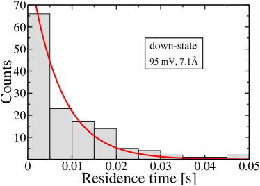
Prior to the measurement of the switching process, the STM tip was stabilized at =-340mV and =0.1nA, corresponding to a tip-surface separation of 10.6Å (Ref. 8), which is outside the regime in which repeated switching is observed. Absolute calibration of the tip-surface separation was done as described in Ref. 8 (error of Å for the absolute height). Time spectra of the current were recorded for different bias voltages and tip-surface separations with the feed-back loop switched off. The time dependent current I(t) is shown in Fig. 2(a) for the applied bias voltage of 95mV and with the tip positioned at 7.1Å above the substrate.
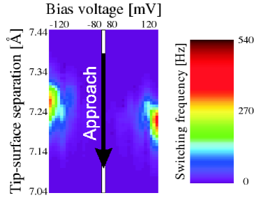
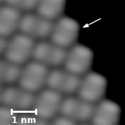
The quantitative analysis of the switching process, which is the primary objective of this paper, has been carried out for molecules located at the edge of a monolayer island of PTCDA/Ag(111) (as indicated with the white arrow in in Fig. 1(b)). The reason for choosing these molecules is that the PTCDA molecules in the midst of a compact layer are more difficult to pick up due to strong intermolecular interactions with neighboring molecules via hydrogen bonds,WeissJACS while isolated molecules do not always fall back to the same position on the surface when they switch from the up- to the down-state, thereby leaving the junction and precluding the continued measurement of the switching time trace.
A color-coded map of the frequency of switching events as a function of bias voltage and tip-surface separation is displayed in Fig. 2(b). We observe the following: (1) Repeated switching occurs for both bias voltage polarities above a threshold of approximately meV. In contrast, for meV a single jump into contact occursPTCDA_Kondo ; Toher1 (not indicated in Fig. 2(b)); for these bias voltages, the junction may only (but does not necessarily) switch back from the up- to the down-state if the tip is retracted again beyond the tip-surface separation at which the jump into contact has originally occured (hysteresis). (2) Repeated switching occurs in a narrow bracket of tip-surface separations in the range from 7.34Å to 7.14Å. (3) The range in which repeated switching is observed appears at slightly larger tip-surface separations for negative bias than for positive bias. This latter fact may be related to the negative polarization of the carboxylic oxgen atoms in Ag(111)-adsorbed PTCDA.
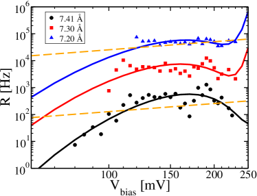
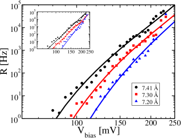
¿From the I(t) curve in Fig. 2(a) one can see that for the chosen bias and tip-surface separation, the up-state is preferred: the statistical residence time analysis (Figs. 2(c) and (d)) reveals a difference of more than one order of magnitude in the residence time values for the high- and low-conductance states. The single exponential behavior of the curves indicates a two state Markovian switching process where the residence time probability density is given by the expression Here, is the transfer rate between the two conductance states. It is obtained by fitting the equation for to the corresponding residence time histogram. By performing such a transfer rate analysis for different bias voltages one can determine the transfer rates as a function of bias for every measured tip-surface separation. The rates for three typical tip-surface separations are displayed in Fig. 3. The tipsurface transfer rate increases monotonically with applied bias in the given voltage range, but the surfacetip transfer rate appears to have a maximum around 180mV. Finally, both rates are dependent on the tip-surface separation, as can also be seen in the experimental data in Fig. 2(b).
III theoretical model
To gain insight into the observed current switching, we first focus on the nature of the coupling between PTCDA and the surface, and then provide a link to the experimental data by applying a model calculation. The mechanisms of the chemical bonding of PTCDA to Ag(111) includes hybridization of the molecular orbitals with the substrate states, charge transfer between the substrate and the molecule, local bonds of the carboxylic oxygens to silver atoms below and an extended bond of the molecular -system to the surface.Pump1 ; tautz07 ; tautz07a ; Kraft Assuming that the two meta-stable positions can be well-represented by a (not necessarily symmetric) double-well potential, the transfer of an adsorbate between the two minima may involve a variety of physical processes, such as (i) thermal activation, (ii) quantum tunneling, (iii) a transition through an electronic excited state with no conformational bi-stability, or (iv) vibrational heating. Process (i) is of minor interest in this work, since the experiments are performed at very low temperatures (5-6 K) and the barrier height is larger than 100meV, which excludes the thermal activation. Due to the relatively large mass of the part of the molecule involved in the switching process, process (ii) is also very improbable. Assuming a tunneling barrier of 100meV height (measured from the vibrational ground state) and 1Å width (cf. Fig. 4(a)) the corresponding tunneling rate for the carboxylic oxygen atom was estimated to be of the order of Hz. For process (iii), which involves an excited state of the molecule, the residence time of the tunneling electrons has to be sufficiently large to induce this excitation. However, since the molecule is chemisorbed on the Ag(111) surface, this residence time is expected to be quite small, so that process (iii) also seems unlikely in this case. Thus, we suggest that the microscopic mechanism leading to switching is related to vibrational heating, where the transition is induced by progressive vibrational excitation of the relevant chemical bond (i.e., either the oxygen-surface bond for the surfacetip process or the oxygen-tip bond for the reverse process) by the inelastic scattering of tunneling electrons, eventually leading to bond breaking. The transition rate is then mainly determined by the competition between energy gain from the tunneling charges and energy losses due to electron-hole pair generation and/or coupling to the substrate phonon continuum.
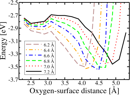
In Ref. 22 Gao et al. developed a theoretical model to describe atomic switching by vibrational heating. They concluded that the switching rate should exhibit a power law dependence on the bias voltage where is the number of vibrational levels that have to be climbed before the switch can occur. In our experiments we observe a striking difference between the tipsurface and surfacetip switching processes as far as the bias dependence of the switching rate is concerned (cf. Fig. 3). While the tipsurface process shows an almost linear behavior in the double logarithmic plot, in essential agreement with the prediction of Ref. 22, a reasonable description within the model of Gao et al.Gao for the surfacetip process is very unlikely, because deviates from a simple power law, showing a saturation of the transfer rate at approximately 120mV, with even a possible maximum around 180mV. Moreover, a (rather poor) fit of the data in Fig. 3(a) with would only be possible by assuming (cf. dashed line in Fig. 3(a)), which is in contrast to the calculated potential energy surfaces, see Fig. 4(a).
Below we show that if the energy dependence of the density of states around the Fermi level is taken into account explicitly, and if in particular different transport orbitals for the two configurations (i.e. up- and down-states) are used, the evident differences between the surfacetip and tipsurface processes can be rationalized and both the data in Figs. 3(a) and (b) can be fitted with parameters which are in qualitative agreement with DFT results for the electronic structure of the molecular junction. In our model, we will neglect the coupling to the substrate phonon continuum, since the anharmonic coupling is, in general, very small at low temperatures.
Our model is a minimal approach based on that used in Ref. 22 to describe the vibrational heating. The Hamiltonian describing the tunneling of electrons between the STM tip and the surface via an adsorbate level (in this case, the adsorbate being the PTCDA molecule) has the following form:
| (1) | ||||
Here , and label one-electron states , and of the surface, the tip and the molecule, respectively, with the corresponding energies , and . The hopping between the surface and the tip via the molecular level is described by the two terms including and . The coupling between the vibrational motion of the molecule and the electron propagating through it can be modeled by:
| (2) |
where,
| (3) |
The coupling is modeled by assuming that is a linear function of the vibrational coordinate , ; is the frequency of the molecular vibration with the normal coordinate and mass , and at .
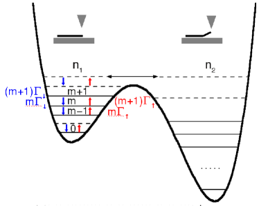
Since the effect of the electron-vibration interaction on the adsorbate electronic states is in general weak, it can be treated by first-order perturbation theory. The assumed linearity in the charge-vibron coupling simplifies the problem since only the excitation and relaxation rates, and , between the vibrational ground state and the first excited state are required (cf. Fig. 4(b)). In first-order perturbation theory these transition rates are given by Fermi’s Golden Rule:
| (4) | ||||
| (5) |
where and are the vibrational ground state and the first excited state respectively, while and denote any of the stationary one-electron states of the tip or the substrate with corresponding Fermi-Dirac distributions , and denotes the electron-vibration interaction (Eq. (2)).
These rates describe the vibrational excitation and relaxation induced by the tunneling electrons. Since the initial and final states of a tunneling electron can be located either in the tip or the substrate, these rates can be decomposed into four different terms: , , and , which sum up to give . Here, the first (second) superscript denotes whether the final (initial) state belongs to the surface or the tip. In contrast to Ref. 22, we will not assume that the adsorbate local DOS is constant over the relevant energy range, but rather we model it by a Lorentzian shape, , where , with and describing the coupling between the molecular level and the substrate and tip electronic states, respectively. Using this function, the excitation and relaxation rates can be calculated analytically in the low temperature limit. We refer the interested reader to appendix A for further details and a comprehensive description of the calculation.
To describe the transfer between the two possible meta-stable states a truncated harmonic oscillator model, as described in Ref. 22, is adopted. The transfer rate can be expressed as a product of the transition into level (see Fig. 4(b)) and an effective Boltzmann factor (with characteristic temperature ) describing the probability to arrive at the sub-critical level where the transition takes place:Gao
| (6) |
Since the adsorbate local DOS is not assumed to be constant over the relevant energy range, the above expression in general does not yield a simple power law dependence on the applied bias as in Ref. 22 (). This simple scaling law can only be recovered, if the molecular level is situated far from the Fermi energy (so that the DOS at is almost constant).
IV results and discussion
Using Eqs. (A1–A4) in the appendix, we are now able to fit the transfer rate in Eq. (6) to the experimental results. Figure 3 shows the fitted transfer rates as a function of bias voltage, together with the experimental data. The corresponding fitting parameters are listed in Tab. 1 and will now be discussed in detail.
The vibrational energies (i.e. the size of the steps on the “vibrational ladder”) were determined from the curvature of the calculated potential energy surfaces, shown in Fig. 4(a). They lie around 19meV for the shallower well of the down-state, and around 40meV for the deeper well of the up-state. The dependence of these vibrational frequencies on the tip–surface distance is negligible (cf. Tab. 1).
The are an output of the fitting of the transfer rates. Multiplied with , they yield the barrier heights for the switching process. The products and in Tab. 1 are consistent with the potential energy surfaces obtained from DFT calculations shown in Fig. 4(a), which exhibit a highly asymmetric double well, with a shallow well for the down-state and a deep one for the up-state. The asymmetry increases as the tip-surface separation is reduced. In particular, the depth of the potential well of the up-state (), which according to Tab. 1 amounts to 0.53eV at 7.3Å, agrees quite well with that calculated within DFT, whereas the model predicts a down-state well of 0.17eV at 7.3Å that is slightly deeper than that derived from the ab-initio calculations (cf. Fig. 4(a)). This may be due to the fact that the potentials in Fig. 4(a) were calculated for a single PTCDA molecule, whereas in the switching experiments edge molecules were used; their hydrogen bonds to neighboring molecules will lead to a significant increase of the barrier height. Note, however, that the model does correctly predict the decrease in depth of the down-state well as the tip-surface separation is decreased; this tendency is due to the reduction of the potential minimum to a saddle point for tip-surface separations of less than about 6.2Å (cf. Fig. 4(a)).
A further important parameter in our model for the transfer rate is the position of energy level through which the electron current that causes the vibrational heating passes (i.e. the transport level), because this influences the energy dependent density of states that enters the rate via Eqs. (4) and (5). It is clear that levels on either side and closest to the Fermi energy are the most important channels for the electron current. Our DFT calculationsToher1 show that mainly states both above and below the Fermi level could contribute, see Fig. 5. The level below is the former LUMO that gets filled on adsorption and that is clearly observed in scanning tunneling spectroscopy.tautz07 ; tautz07a ; Kraft The sharp level above that is found in DFT appears in experiments as a broader feature in the gap between the former LUMO and the LUMO+1, especially for molecules at the edges of monolayer islands. In our minimal model Hamiltonian we can only take one transport level into account. It turns out that the qualitatively different behavior of the two processes surfacetip and tipsurface requires the use of two different transport levels, depending on the switching direction. This is reflected in Tab. 1 by negative values for the tipsurface process, while the surfacetip process has positive values (the spectral density of the levels and are shown in Fig. 6). In other words, we have to assume that in the up-state the switching current passes mainly through occupied DOS of the junction, whereas in the down-state it passes predominantly through the empty DOS of the adsorbed molecule. Note that due to the way in which the bias voltage drops between tip and substrate, both molecular levels and are within the bias window and may in principle contribute to the transport, but in our minimal model we can – as mentioned above – only take one into account at a time.
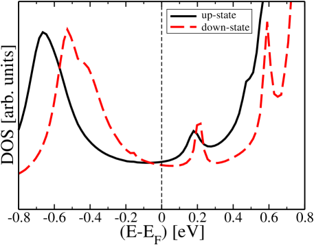
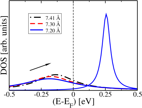
The fitted values show a clear tendency to move up towards the Fermi level as the tip-surface separation is increased. This tendency is known very well both from experimentPTCDA_Kondo and DFT calculations,Pump1 ; Toher1 although the precise level positions in experiment and ab initio theory differ from those in Tab. 1. This is not too surprising since our minimal model only allows for a single Lorentzian level whereas the actual density of states is much more complicated. The fitted values range between 0.24eV and 0.30eV, whereas the DFT calculation has this level fixed at 0.2eV.
The small decrease in the transfer rate of the surfacetip process at about 220meV (Fig. 3(a)) is due to the molecular level entering into resonance with the Fermi energy of the STM tip, which leads to a reduction of the vibrational lifetimes of the PTCDA molecule in the junction (i.e. the rate at which the molecular vibrational energy dissipates into the electrodes is increased, cf. Eqs. (A1, A4)). This in turn reduces the transfer rate of the molecule between the surface and the tip. Further raising the bias voltage beyond this point results in the transfer rate increasing once again due to non-resonant tunneling. We stress that this behavior can only be obtained if an energy-dependent DOS is used; a constant DOS could not yield such a behavior. Unfortunately, the increase above 240meV cannot be observed in the experiments since the molecule normally disintegrates at lower biases than this because of the high current density.
| Tip–surface distance | |||||||
| Å | |||||||
| Å | |||||||
| Å | |||||||
| Å | |||||||
| Å | |||||||
| Å | |||||||
| Å | |||||||
| Å | |||||||
| Å | |||||||
| Å | |||||||
| Tip–surface distance | |||||||
| Å | |||||||
| Å | |||||||
| Å | |||||||
| Å | |||||||
| Å | |||||||
| Å | |||||||
| Å | |||||||
| Å | |||||||
| Å | |||||||
| Å |
V conclusion
In summary, switching between low- and high conductance states has been observed in a single molecule junction consisting of a PTCDA molecule on a Ag(111) substrate and contacted by an STM tip. The rates for the transition between these two states can be sensitively tuned by varying the applied bias as well as the tip-surface separation. A vibrational heating mechanism where molecular bonds are excited by tunneling charges has been proposed to interpret the experimental results. Switching rates were calculated within a minimal model Hamiltonian approach describing the interaction between tunneling electrons and local molecular vibrations. The experimental results could be fitted over a broad voltage range for the cases where the PTCDA molecule switches both from the surface to the tip and from the tip to the surface. In particular, the non-monotonic behavior of the surface to tip switching rate could only be described by modeling the DOS by Lorentzian functions instead of assuming it to be energy independent, as has been the usual practice in the literature until now. This demonstrates that it is crucial to take the non-constant behavior of the molecular DOS into account.
Acknowledgements.
This work has been supported by the German Priority Program “Quantum transport at the molecular scale (SPP1243)”. The authors acknowledge the Center for Information Services and High Performance Computing (ZIH) at the Dresden University of Technology for computational resources. GC acknowledges the South Korean Ministry of Education, Science, and Technology Program, Project WCU ITCE No. R31-2008-000-10100-0. TB would like to acknowledge an especially fruitful discussion with Florian Pump.Appendix A Calculation of the transition rates
In the following we want to sketch the derivation of the transition and relaxation rates. The terms and are all similar, and it is sufficient to calculate explicitly only the term . Inserting the electron-vibration interaction (Eq. (2)) into Eq. (5) together with the expression for the molecular DOS gives
| (7) |
In the first step the sum over states has been replaced with an integral over by introducing . In the second step the expression for the molecular DOS was used to rewrite the local density of states. Since the STM experiments are carried out at 5-6 K one can approximate the Fermi function with the Heaviside step function in the next step. Thus, the limits of the integral can be changed from and to or respectively. The influence of an applied bias can be easily introduced by shifting the Fermi level of the surface , where is the Fermi level at of the surface. Since we used the low temperature approximation in step 3 of Eq. (A1) the excitation rates become zero, because of the Pauli exclusion principle. The Pauli exclusion principle also simplifies the calculation of the remaining terms and , which describe the transition rates due to the inelastic scattering of tunneling electrons between surface and tip. Assuming , for positive applied bias the tunneling from surface to tip through the adsorbate level is prohibited. The excitation is forbidden because all states at the tip are occupied up to the energy , thus making it impossible for an electron from the surface with energy to tunnel to the tip. The probability of relaxing an adsorbate vibrations due to the inelastic scattering of tunneling electrons from the surface to the tip is negligibly small, because the scattered electron would need several to gain enough energy. But this process can also be excluded, since the electron-vibration interaction on the adsorbate vibration is in general weak and we treat it by first-order perturbation theory. Thus, the transition rates can be written as, e.g.
| (8) |
| (9) |
| (10) |
The parameter given in Eq. (3) is an important parameter in our theory, as one can clearly see in the Eqs. (A1–A4). In contrast to all other parameters, e.g. the broadening or the energy , it is in general difficult to determine it from experiment or ab-initio calculations. However, these are only prefactors which change the absolute magnitude of the transition rates and thus can be easily fitted to the experiments.
References
- (1) G. Binnig, H. Rohrer, Ch. Gerber and E. Weibel, Phys. Rev. Lett. 49, 57 (1982).
- (2) F. Moresco, Phys. Rep. 399, 175 (2004).
- (3) N.J. Tao, Nat. Nanotechnol. 1, 173 (2006).
- (4) R. Temirov, A. Lassise, F. Anders, and F.S. Tautz, Nanotechnology 19, 065401 (2008).
- (5) F. Pump, R. Temirov, O. Neucheva, S. Soubatch, S. Tautz, M. Rohlfing, and G. Cuniberti, Appl. Phys. A 93, 335 (2008).
- (6) L. Lafferentz, F. Ample, H. Yu, S. Hecht, C. Joachim and L. Grill, Science 323, 1193 (2009).
- (7) S. Chang, J. He, S. Kibel, M. Lee, O. Sankey, P. Zhang and S. Lindsay, Nature Nanotechnol. 323, 1193 (2009).
- (8) C. Toher, R. Temirov, A. Greuling, F. Pump, M. Kaczmarski, G. Cuniberti, M. Rohlfing, and F.S. Tautz Phys. Rev. B 83, 155402 (2011).
- (9) D. Eigler and E. Schweizer, Nature 344, 524 (1991).
- (10) A.J. Heinrich, C.P. Lutz, J.A. Gupta, and D.M. Eigler, Science 298, 1381 (2002).
- (11) J.A. Stroscio and R.J. Celotta, Science 306, 242 (2004).
- (12) F. Moresco, G. Meyer, K.-H. Rieder, H. Tang, A. Gourdon, and C. Joachim, Phys. Rev. Lett. 86, 672 (2001).
- (13) J.A. Stroscio, F. Tavazza, J.N. Crain, R.J. Celotta, and A.M. Chaka, Science 313, 948 (2006).
- (14) V. Iancu and S.-W. Hla, Proc. Natl. Acad. Sci. 103, 13718 (2006).
- (15) K.R. Harikumar, J.C. Polanyi, P.A. Sloan, S. Ayissi, and W.A. Hofer, J. Am. Chem. Soc. 128, 16791 (2006).
- (16) P. Liljeroth, J. Repp, and G. Meyer, Science 317, 1203 (2007).
- (17) R. Ohmann, L. Vitali and K. Kern, Nano Lett. 10, 2995 (2010).
- (18) S.G. Tikhodeev and H. Ueba, Phys. Rev. B 70, 125414 (2004).
- (19) H. Ueba, T. Mii, N. Lorente, and B.N.J. Persson, J. Chem. Phys. 123, 084707 (2005).
- (20) S.G. Tikhodeev and H. Ueba, Phys. Rev. Lett. 102, 246101 (2009).
- (21) M. Cizek, M. Thoss, and W. Domcke, Phys. Rev. B 70, 125406 (2004).
- (22) S. Gao, M. Persson, and B. Lundqvist, Phys. Rev. B 55, 4825 (1997).
- (23) F. Elste, G. Weick, C. Timm, and F. von Oppen, Appl. Phys. Mater. Sci. Process. 93, (2008).
- (24) L.J. Lauhon and W. Ho, Phys. Rev. Lett. 85, 4566 (2000).
- (25) K. Glöckler, C. Seidel, A. Soukopp, M. Sokolowski, E. Umbach, M. Böhringer, R. Berndt, and W. D. Schneider, Surface Science 405, 1 (1998).
- (26) F.S. Tautz, Prog. Surf. Sci. 82, 479 (2007).
- (27) M. Rohlfing, R. Temirov, and F.S. Tautz, Phys. Rev. B 76, 115421 (2007).
- (28) A. Kraft, R. Temirov, S.K.M. Henze, S. Soubatch, M. Rohlfing, F.S. Tautz, Phys. Rev. B 74, 041402 (2006).
- (29) C. Weiss, C. Wagner. R. Temirov, and F.S. Tautz J. Am. Soc. Chem. 132, 11864 (2010)