An in-situ tunable radio-frequency quantum point contact
Abstract
Incorporating a variable capacitance diode into a radio-frequency matching circuit allows us to in-situ tune the resonance frequency of an RF quantum point contact, increasing the versatility of the latter as a fast charge sensor of a proximal quantum circuit. The performance of this method is compared in detail to conventional low-frequency charge detection. The approach is also applicable to other RF-detection schemes, such as RF-SET circuits.
pacs:
73.23.Hk, 07.50.Qx, 85.35.BeEmbedding single electron transistors (SETs) schoelkopf:98 ; *lu:03, quantum point contacts (QPCs) qin:06 ; mueller:07 ; reilly:07 ; *barthel:09; cassidy:07 , and quantum dots (QDs) barthel:10 into radio-frequency (RF) matching circuits has become a successful technique for fast and sensitive charge read-out of quantum dot circuits. The large measurement bandwidths of these methods potentially allow for probing processes at timescales beyond the scope of conventional charge sensing, and, more straightforwardly, drastically reduce the time required for “standard” measurements.
While lumped element matching networks are being used as a reliable method for achieving accurate matching, their components are up to now static and do not allow for fine-tuning once the system is cold for measurement. As the circuit parameters are different at low compared to room temperatures, good matching at room temperature will generally not lead to the same resonance quality after cooling down. Hence it can be a complex and time-consuming endeavor to obtain high-quality matching at low temperatures for new samples. Using a variable capacitance diode as a capacitor in series to a parallel -circuit Note:CLCR enables us to in-situ tune the resonant frequency and hereby also the QPC conductance for which optimal matching is obtained by applying a voltage across the diode Note:Diode . Notably, if the measurement setup suffers from standing waves, we can set the resonance frequency to an anti-node, avoiding signal loss due to destructive interference.

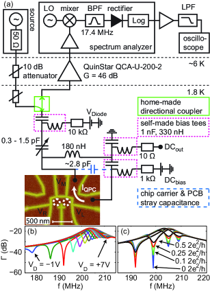
The measurement setup for our variable temperature insert at is shown in Fig. 1(a). A radio-frequency signal of about 200 MHz is applied, attenuated at low temperatures, and reflected at the lumped-element matching network containing the QPC Note:Socket . The reflected voltage is amplified by 46 dB at low temperatures using a commercial cryogenic low noise amplifier Note:LNA and analyzed using a network/spectrum analyzer Note:RS , offering adjustable room temperature amplification and high-quality intermediate-frequency filtering. Simultaneous DC measurements can be performed via self-made bias tees on the matching chip.
A double quantum dot with integrated charge sensor (see Fig. 1) was fabricated on a GaAs/Al0.3Ga0.7As heterostructure with a two-dimensional electron gas 34 nm below the surface (, ) by atomic force microscopy lithography fuhrer:02 . Charging an electron into the right dot leads to a change in QPC conductance of approximately . This value is unusually low for AFM lithography designed samples, probably due to the elevated temperature and the location where the charge detector QPC is formed.
Figure 1(b) shows the tunability of the resonance frequency by applying a voltage to the variable capacitance diode. With voltages in the range of -1 to +7 V Note6 we shift the resonance frequency by more than 30 MHz. From one curve to the next, the voltage is increased by 0.5 V, with the QPC conductance fixed at . In Fig. 1(c), the QPC’s conductance is taking the values 0 (blue), 0.1 (green), 0.25 (red), and (black) for different resonant frequencies (given by V). For V, a closed QPC leads to the best matching, whereas for V, minimal reflection is obtained for . Hence we can not only tune the resonance frequency, but also achieve matching at a desired QPC conductance. Figures 1(b) and (c) exhibit a strong background due to a standing wave between matching circuit and cold amplifier. Destructive interference significantly reduces the reflected power for certain frequencies.

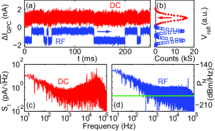
A time trace of dot-lead charging is shown in Fig. 2(a), with all measurement parameters optimized as explained later-on. The DC current was measured using an IV-converter with a feedback resistor of 1 M in order to ensure a large enough setup bandwidth. The reflected RF voltage was rectified and logarithmically amplified (video signal) with a spectrum analyzer. DC and RF signals have been sampled with an oscilloscope and 8th order Bessel lowpass filtered at 50 kHz by software. While the RF signal clearly exhibits steps whenever an electron hops into and out of the right dot, the DC signal is completely drowned in noise, the positions of the charging events can only be guessed.
The histograms of these traces lead to the distributions given in Fig. 2(b). While the histogram of the RF signal reveals two distinct peaks separated by , the width of the DC current distribution is much larger than the difference of the peak positions .
Figures 2(c,d) show the spectral densities of the DC and RF time traces in (a), lowpass filtered at 100 kHz. The decrease up to frequencies of 1 kHz in both spectra originates from the random telegraph signal itself. Beyond that, the RF spectrum is essentially flat, while the DC spectrum exhibits a significant increase for frequencies above a few kHz. This so-called capacitive noise gain stems from the unavoidable capacitance of the sample cables ( nF) and can only be reduced by putting the IV-converter or an FET-based amplifier closer to the sample vink:07 ; hayashi:09 . For frequencies above 50 kHz, the DC spectrum decreases due to a lowpass filter set by the feedback resistor and its shunt capacitor, introduced to cut off the capacitive noise gain, in combination with the finite gain-bandwidth product of the operation amplifier. Increasing the feedback resistor to 10 M decreases this value to approximately 10 kHz, but slightly improves the noise level. At a bandwidth of 50 kHz, the RF setup clearly performs better, and the higher the potential bandwidth (i.e. the larger the QPC signal) the more favorable the RF technique will turn out to be.

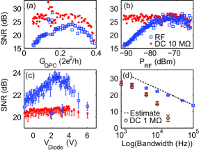
In order to find the optimal read-out parameters for both, conventional and high-frequency techniques, the signal to noise ratio (SNR) of a trace of charging events (see Fig. 2(a) and (b)) is determined for different conditions. The SNR is given in dB, as the logarithm of the signal power divided by the squared standard deviation of the histogram peaks and respectively. Reliable counting of charging events gustavsson:06 using a simple threshold requires a SNR of dB (). A more involved, iterative method, can lower this number drastically yuzhelevski:00 . Unless mentioned, the time traces were lowpass filtered at 1 kHz to obtain a large enough SNR.
Figure 3(a) shows the SNR measured simultaneously with DC (red dots) and RF (blue squares) detection for changing QPC conductance. A DC bias voltage of 250 and an RF power of -80 dBm were applied, both small enough not to significantly influence the other detection method. The diode voltage was set to 2.7 V, fixing the resonant frequency at roughly 205 MHz. For both signals, there is a maximum slightly below , with the RF values decreasing faster at low conductance. At there is an additional occupancy level (probably defect charging) leading to an overestimation of the signal height and hence too large SNR.
Choosing the optimal QPC conductance and varying the applied RF power yields Fig. 3(b). The SNR increases for larger input power, saturating above dBm, where heating sets in, flattening out the QPC curve. From a similar analysis of DC bias voltage (not shown), we found the threshold of the SNR saturation to be 300 , indicating that -75 dBm corresponds to roughly 300 V.
Keeping the optimal QPC conductance and setting the RF and DC bias to the values mentioned above, the influence of the diode voltage (resonance frequency) was investigated (Fig 3(c)). Each point is the average over 10 independent time traces. While the DC SNR is unaffected, the RF SNR exhibits a maximum for voltages between 2 and 3 V, with resonant frequencies slightly above 200 MHz. This maximum does not occur at the best matching setting, but at the anti-node of the standing wave (see Fig. 1). For other frequencies, a significant part of the signal cancels out. If the input of the cryogenic amplifier would be perfectly matched, or if one could mount a matched circulator Note7 between resonant circuit and amplifier, a significantly reduced standing wave is to be expected and the highest SNR would be obtained for best matching. The input power is fixed for all diode capacitances, leading to different voltage drops over the QPC. By monitoring the QPC current, we can ensure that the QPC’s power dissipation does not significantly change in our range of diode voltages. We observe a slight increase () of current at the anti-node, though. As the input power limit was determined for a resonance frequency at the anti-node Note8 , we are led to conclude that removing the standing wave will increase the SNR ratio at optimal matching by 10 dB, the height of the standing wave.
With all parameters optimized, we varied the software low pass filter frequency in order to find the maximum measurement bandwidth achievable with both methods. The result is shown in Fig. 3(d). For low bandwidth (few kHz), DC - with 1 M (brown circles) as well as 10 M feedback resistance - and RF perform comparably. Capacitive noise gain deteriorates the DC SNR for larger bandwidth. An I/V-converter feedback resistor of 10 M inherently limits the DC bandwidth to approximately 10 kHz. Lowering this value to 1 M increases this cutoff to 50 kHz at the cost of a slight loss in SNR even at low bandwidth. As the RF noise spectrum is flat above a few kHz, the expected linear decrease of SNR with increasing bandwidth (dashed line) can be observed. For a detection bandwidth of 50 kHz, the RF SNR is already higher by more than a factor 10. From the decrease of the SNR at high frequencies we can estimate the maximal bandwidth for a SNR of unity (0 dB) to be 2.5 MHz, yielding a charge sensitivity of , comparable to values reported by other groups using fast QPC charge sensors reilly:07 ; *barthel:09; cassidy:07 ; vink:07 . The charge sensitivity with the DC technique is - an order of magnitude lower. As observed by others, lowering the temperature considerably increases the sensitivity at low source-drain bias cassidy:07 . As charge sensitivity scales linearly with the coupling of the dot to the QPC, using a self-aligned charge read-out QPC on an InAs nanowire quantum dot shorubalko:08 should boost the sensitivity by a factor of and therefore the single shot measurement bandwidth by almost a factor 50.
In conclusion we have demonstrated in-situ tunability of a lumped-element matched RF QPC. Its performance was compared to conventional charge sensing after both methods were optimized with respect to the QPC’s conductance, RF power and DC voltage, as well as resonance frequency (varactor diode capacitance) of the matching circuit. A good charge sensitivity of was achieved in spite of the elevated temperature of 2 K. Reduction of standing waves in the experimental setup as well as increasing the dot-to-QPC coupling can further improve this value.
We thank P. Leek and A. Wallraff for technical advice and are grateful to S. Gustavsson for the measurement software. Our research was funded by the Swiss National Science Foundation (SNF).
References
- (1) R. J. Schoelkopf, P. Wahlgren, A. A. Kozhenikov, P. Delsing, and D. E. Prober, Science 280, 1238 (1998)
- (2) W. Lu, J. Zhongqing, L. Pfeiffer, K. W. West, and A. J. Rimberg, Nature 423, 422 (2003)
- (3) H. Qin and D. A. Williams, Appl. Phys. Lett. 88, 203506 (2006)
- (4) T. Müller, K. Vollenweider, T. Ihn, R. Schleser, M. Sigrist, K. Ensslin, M. Reinwald, and W. Wegscheider, AIP Conf. Proc. 893, 1113 (2007)
- (5) D. J. Reilly, C. M. Marcus, M. P. Hanson, and A. C. Gossard, Appl. Phys. Lett. 91, 162101 (2007)
- (6) C. Barthel, D. J. Reilly, C. M. Marcus, M. P. Hanson, and A. C. Gossard, Phys. Rev. Lett. 103, 160503 (2009)
- (7) M. C. Cassidy, A. S. Dzurak, R. G. Clark, K. D. Petersson, I. Farrer, D. A. Ritchie, and C. G. Smith, Appl. Phys. Lett. 91, 222104 (2007)
- (8) C. Barthel, M. Kjærgaard, J. Medford, M. Stopa, C. M. Marcus, M. P. Hanson and A. C. Gossard, Phys. Rev. B 87, 161308 (2010)
- (9) The parallel inductance and capacitance transform the small real-valued conductance of the QPC to a complex admittance with large modulus that is dominated by the coil. The imaginary part of this combined impedance is compensated for by the tunable capacitance in series and only the small real value close to remains.
- (10) This voltage changes the length of the depletion layer of the GaAs -junction (MA-COM MA46H070).
- (11) Contrary to predominant matching techniques, the QPC is not directly bonded to the matching circuit, but sits in a chip socket, soldered to the high-frequency printed circuit board (pcb) containing the matching circuit. This suffers from larger chip stray capacitance ( pF) but increases the versatility of the setup, as the sample does not have to be designed to fit the pcb. In particular, the setup is compatible with samples fabricated for conventional platforms. See also L. J. Taskinen, R. P. Starrett, T. P. Martin, A. P. Micolich, A. R. Hamilton, M. Y. Simmons, D. A. Ritchie, and M. Pepper, Rev. Sci. Instr. 79, 123901 (2008).
- (12) QuinStar QCU U-200-2
- (13) RohdeSchwarz ZVL/FSL 6
- (14) A. Fuhrer, A. Dorn, S. L scher, T. Heinzel, K. Ensslin, W. Wegscheider, and M. Bichler, Superlattices and Microstructures 31, 19 (2002)
- (15) More negative voltages lead to direct current through the forward biased -junction, more positive voltages do not alter the diode’s capacitance in a significant way.
- (16) I. T. Vink, T. Nooitgedagt, R. N. Schouten, L. M. K. Vandersypen, and W. Wegscheider, Appl. Phys. Lett. 91 123512 (2007)
- (17) K. Hayashi, K. Saitoh, Y. Shibayama, and K. Shirahama, J. of Physics: Conf. S. 150 012016 (2009)
- (18) S. Gustavsson, R. Leturcq, B. Simovič, R. Schleser, T. Ihn, P. Studerus, K. Ensslin, D. C. Driscoll, and A. C. Gossard, Phys. Rev. Lett. 96 076605 (2006)
- (19) Y. Yuzhelevski, M. Yuzhelevski, and G. Jung, Rev. Sci. Instr. 71, 1681 (2000)
- (20) In our variable temperature insert, space is too limited. In a standard dilution refrigerator however, this is easily done.
- (21) At good matching, the power dissipated over the QPC is given by the input power and barely influenced by the standing wave.
- (22) I. Shorubalko, R. Leturcq, A. Pfund, D. Tyndall, R. Krischek, S. Schön, and K. Ensslin, Nano Letters 8, 382 (2008)