Mechanism for graphene-based optoelectronic switches by tuning surface plasmon-polaritons in monolayer graphene
Abstract
It is shown that one can explore the optical conductivity of graphene, together with the ability of controlling its electronic density by an applied gate voltage, in order to achieve resonant coupling between an external electromagnetic radiation and surface plasmon-polaritons in the graphene layer. This opens the possibility of electrical control of the intensity of light reflected inside a prism placed on top of the graphene layer, by switching between the regimes of total reflection and total absorption. The predicted effect can be used to build graphene-based opto-electronic switches.
pacs:
81.05.uepacs:
72.80.Vppacs:
78.67.WjGraphene Electronic transport in graphene Optical properties of graphene
Among the many promised graphene dreams [1, 2, 3], the possibility of exploring the electronic, thermal, and mechanical properties of graphene, having in view a new generation of optoelectronic devices, is one of the most exciting of those dreams. Understanding the fundamental physics of the interaction of electrons (in graphene) with an electromagnetic field is a key step toward the realization of such devices.
The optical response of graphene has been an active field of research, both experimental [4, 7, 5, 6] and theoretical [8, 9, 10], and much is already understood. From the theoretical point of view, the independent electron approximation predicts that the real part of optical conductivity of graphene, at zero temperature, has the form , where is the AC universal conductivity of graphene, is the photon energy, is the chemical potential, and is the Heaviside step function. The imaginary part of the conductivity is finite everywhere, as long as is also finite [11]. For zero chemical potential, the experiments [4, 7, 5] confirm the independent electron model predictions. On the other hand, for finite chemical potential and , the experiments show a substantial absorption in this energy range, at odds with the theoretical prediction. In simple terms, the real part of the conductivity, as measured experimentally, follows roughly the formula , where is the energy at which the Drude peak starts developing. Below , the optical response increases dramatically. The difference between experiment and theory can be explained by both inter-band and intra-band scattering, due to impurities and electron-electron interactions. In what concerns our present study, the deviations seen in the experimental data are actually vital for the effect we discuss below, and therefore the calculations we present below use the experimentally measured conductivity of graphene. The exact form of below the threshold is essential for the particular type of interaction of the electrons in graphene with an electromagnetic field leading to the formation of surface plasmon-polaritons [12].
Surface plasmon-polariton (SPP) is an evanescent electromagnetic wave induced by the coupling of the electromagnetic field to the electrons near the surface of a metal or a semiconductor. Its amplitude decays exponentially at both sides of the interface. The SPP properties are determined by the dielectric function of the conductor (which is related to the optical conductivity) and the dielectric constants of the surrounding media [12, 13]. Clearly, graphene is the ultimate thin surface layer. This fact, together with the ability of tuning the value of the chemical potential by an external gate, makes this system particularly interesting, since the formation of this type of electromagnetic surface waves can by controlled externally.
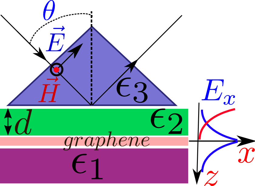
From the point of view of applications, surface plasmon-polaritons can be explored in plasmon sensors [14] and high-resolution imaging [15], as well as for the miniaturization of photonics components [16, 17, 18]. In this Letter, we show that it is feasible to achieve a sharp resonance of the attenuation of an electromagnetic wave by transferring its energy into the excitation of surface plasmon-polaritons in graphene. Indeed, our results demonstrate that, by adjusing the external gate voltage of an attenuated total internal reflection (ATR) structure with graphene layer, it is possible to tune, reversibly, the reflectance of the incident electromagnetic wave from total absorption to total reflection. The structure including a graphene layer, considered in the calculations presented below and suitable for the SPP excitation in graphene is shown in Fig. 1 where the necessary definitions are given.
The geometry of the experimental setup depicted in Fig. 1 is known as ATR configuration. The key point is to shine light on the prism at an angle larger than the critical angle () for total internal reflection, characteristic of the interface between the prism and the dielectric underneath (which can be an air gap or a dielectric layer deposited on top of graphene). From Snell’s law, we have ; choosing large , can be made small thus allowing for a broad range of angles, , to be scanned. Since graphene is at a finite distance from the reflecting interface, it is possible to transfer the energy of the incoming light to the SPP excitation via frustrated (or attenuated) total internal reflection. To compute the electromagnetic response of such a system, we need to solve Maxwell equations in the presence of the three dielectrics, with graphene acting as a conductive surface. The mathematical procedure is well known [13] but the calculations are lengthy (we shall outline the derivation procedure below). The central result of this Letter is the equation defining the reflectance of an incoming electromagnetic wave using the ATR effect, with this quantity defined as and being the complex reflection coefficient given by
| (1) |
where
| (2) | |||
| (3) |
In Eq. (1) () with
| (4) |
denoting the in-plane component of the photon wavevector, , and is the speed of light in vacuum. In what follows we will discuss the physical effects implied by Eq. (1) and how they can be used to build a graphene-based optoelectronic switch.
At resonance between the incident wave and SPP, the amplitude of the reflected wave is minimal and, if the dielectric constants are all real, the reflectance vanishes, that is . At the same time, the SPP amplitude, determined by the field in the medium 2, is given by
| (5) |
with denoting the denominator of Eq. (1). The SPP-light coupling in graphene can also be understood from the following simplified picture. In the case of , the condition reduces to
| (6) |
which gives the dispersion relation for the SPP excitations in graphene surrounded by two semi-infinite media ( and ). The dispersion curve , determined by Eq. (6), allows for a qualitative analysis of the SPP properties and the conditions for their excitation. We note that in Eq.(6) the wavevector component along the direction, , is complex and its imaginary part describes the decay of the electromagnetic wave along the graphene sheet. If there were no dissipation in the graphene layer (i.e. if ), SPP would be a nondecaying wave with a purely real wavevector (), propagating along with a phase velocity , smaller than the speed of light in either of the surrounding dielectrics, that is . In reality, SPP is decaying because of the energy dissipation in graphene () and the product must be positive. It follows from Eq. (6) that the condition is satisfied only when . This is a qualitative criterium for the existence of SPPs in the considered structure. Our numerical results presented in Figs. 2(a) to 2(d) confirm that for SPPs in graphene the above criterium indeed works. From these figures we can see that as increases the real part of the wavevector () initially increases (hence, SPPs possess a positive group velocity) and then it reaches a maximum and starts decreasing (here the group velocity is negative). Finally it comes to zero at a critical frequency where the imaginary part of the conductivity vanishes, . Notice that there is a second SPP band at (where is another critical frequency, ), separated by a finite gap from the lower band [Figs. 2(a) to 2(d)]. The gap corresponds to the frequency range and it is precisely where the imaginary part of the conductivity of graphene is negative and SPPs cannot exist, according to the above criterium. The imaginary part of the wavevector increases with the frequency in each of the SPP bands and has its maximum in the vicinity of . By decreasing the chemical potential the maximum values of and also decrease [compare Figs. 2(a) and 2(b), as well as Figs. 2(c) and 2(d)]. The same result can be achieved by decreasing the dielectric constants of the surrounding media. For instance, when the graphene layer is deposited on the SiO2 substrate with for the frequency range relevant to our situation [see Figs.2(a),2(b)] the maxima of and are higher than in the case of vacuum [Figs.2(c),2(d)].
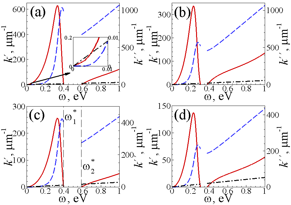
Passing to the description of excitation problem, this can be seen as a coupling of the exponential tails of the electromagnetic wave in the prism and SPPs in graphene, similar to the tunneling effect. We notice that now the in-plane wavevector of the radiation in the prism is a real value defined by its frequency, the angle of incidence and the dielectric constant of the prism material, as expressed by relation (4) and known as ATR scan line. The resonant coupling occurs when the ATR scanline crosses the SPP dispersion curve [see inset in Fig. 2(a)]. The value of at the crossing point determines the quality factor of the resonant excitation and, hence, the relative amplitude of the excited SPP, . Consequently, the efficient SPP excitation is only possible at small values of , because the large hampers the excitation in the vicinity of . Since the imaginary part of the optical conductivity of graphene depends on the gate-controlled chemical potential (for example, at low frequencies, , [11]), it is clear from Eq. (6) that the resonance can be tuned by changing the gate voltage applied to the graphene layer. It should be borne in mind, however, that the true position and the width of the resonance can be found only considering the whole system shown in Fig. 1 and including the real part of the optical conductivity of graphene.
Figure 3 shows a particular example of ATR via coupling to the gated graphene layer at work.
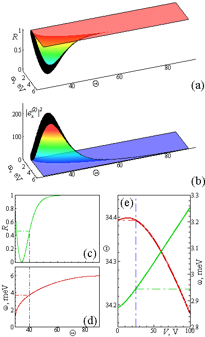
In panels (a)–(d) of this figure, the gate voltage of the capacitor made of a graphene layer as one plane of the plates of the field effect transistor is kept constant. Panel (a) shows the minimum value of at a particular value of the pair of variables and that can be controlled independently. Comparison of panels (a) and (b) demonstrates that resonance minimum of reflectance corresponds to the maximal amplitude of the excited SPP. In other words, these reflectance minima occur as a result of the transformation of the incident wave energy into the energy of SPPs, excited in graphene. It is clear that the value of can be made very small and even zero by an appropriate choice of and as depicted in panels (b) and (c). As we move along the curve of panel (c), by changing the angle , the value of at that angle depends on the frequency of the incoming light. The value of , corresponding to the minimum of the reflectivity , can be read off from panel (d) by drawing a straight vertical line crossing both (c) and (d) panels; an example of such a line is given in Fig. (3). In panel (e) we set and observe how the values of (left axis) and (right axis), change as functions of the gate voltage. For a given gate voltage, a vertical line is drawn intersecting both and curves and the pair of these two variables giving is read off from the corresponding vertical axis. From this panel, we see that it is always possible to find a pair of and satisfying the condition for total absorption. Of course, it is possible to draw the corresponding curves for any given value of . Thus, we can see that indeed it is possible to tune externally the resonance absorption condition by changing the external gate voltage. We would like to stress at this point that it is feasible to implement the predicted resonance absorption effect using large area graphene samples grown by chemical vapor deposition (CVD) [19, 20], since also in this case the optical conductivity of graphene does not change substantially from that of exfoliated produced samples. Since the CVD method allows graphene to be transferred to different substrates, it is also feasible to realize the ATR structure depicted in Fig. 1.
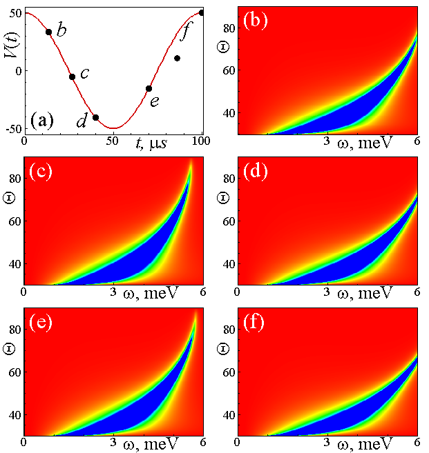
The possibility of changing the chemical potential in graphene by applying a gate voltage makes it possible to tune the ATR conditions by changing this latter quantity, similar to the tuning of the plasmon spectrum as proposed in Ref. [21]. Fig.4 demonstrates the variation in time of the reflectivity of the ATR structure as the function of frequency and angle of incidence. The gate voltage is changed adiabatically according to the harmonic law , with the frequency kHz [Fig.4(a)]. As it can be seen from Fig.4, a decrease of the absolute value of gate voltage corresponds to a shift of the polaritonic resonance to the low-frequency region [e.g., compare Fig.4(b) and 4(c), as well as Fig.4(d) and 4(e)] and a broadening of the resonance.
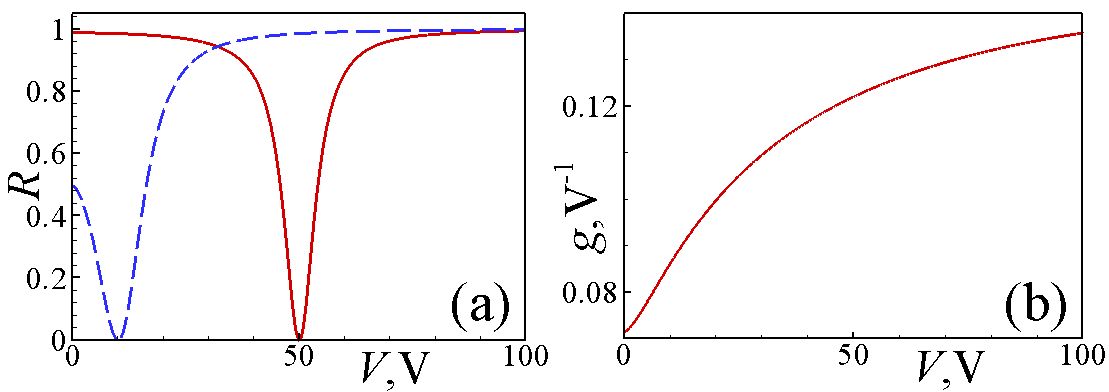
Now a natural question arises: how sensitive is the reflectance of the ATR structure to the variation of gate voltage, when frequency and angle of incidence are fixed? The answer follows from Fig. 5(a), which demonstrates the possibility of changing the ATR structure’s reflectivity from zero to almost unity (full reflectance) by varying the gate voltage within a range of V. As a result, the ATR structure with graphene layer can operate as a switch of electromagnetic radiation in the terahertz domain, where the intensity of the reflected electromagnetic wave can be tuned by the gate voltage, applied to graphene. An important characteristic of the THz switch is the sharpness of the resonance, , which is analogous to the cross-conductivity of a field-effect transistor, calculated as the derivative at the level . As one can see from Fig. 5(b), shows an increase with and then saturates at V.
We shall now present the derivation of our main result. The solution of Maxwell equations , for the -polarized wave can be written in the form:
The meaning of the coefficients is different for the different media. Since in the medium 3 the electromagnetic wave is propagating in -direction, is imaginary [], and the coefficients , are proportional to the amplitudes (at ) of the reflected and incident waves, respectively. In the media 2 and 1 the electromagnetic waves are exponentially decaying along the -axis, and are real (). In the medium 2, the coefficients are superpositions of the electric and magnetic fields at boundary . In the medium 1, the coefficient , while stands for the electric field amplitude at . Boundary conditions at imply the continuity of the tangential components of the electric and magnetic fields, [, ]. At the tangential component of the electric field is continuous , while the discontinuity of the tangential component of the magnetic field, , stems from the presence of surface currents (caused by the SPP electric field) in the graphene layer. Matching these boundary conditions, we obtain a system of linear equations for the field amplitudes in the matrix form,
| (16) |
where , , and . Solution of (16) yields the reflection coefficient [Eq. (1)] and the field amplitude in the gap [Eq. (5)].
To conclude, we have demonstrated that the ATR structure incorporating a monolayer graphene sheet can operate as THz switch where the reflectance of an electromagnetic wave can be switched from nearly unity to nearly zero by applying an external gate voltage to the graphene layer. Since the typical frequencies are meV (or THz, which corresponds to mm of wavelength in vacuum), this structure can operate in the submillimeter range. The frequency of excited SPPs can be increased by using a prism material with a higher dielectric permeability . The proposed device can also be used for spectroscopy of the graphene optical conductivity [22] through measuring the characteristics of the ATR-excited SPPs.
References
- [1] \NameGeim A. K. \REVIEWScience32420091530.
- [2] \NameService R. F. \REVIEWScience3242009877.
- [3] \NamePeres N. M. R. \REVIEWEurophysics News40200917.
- [4] \NameKuzmenko A. B. et al. \REVIEWPhys. Rev. Lett.1002008117401.
- [5] \NameKin Fai Mak et al. \REVIEWPhys. Rev. Lett.1012008196405.
- [6] \NameLi Z. Q. et al. \REVIEWNature Phys.42008532.
- [7] \NameNair R. R. et al. \REVIEWScience32020081308.
- [8] \NamePeres N. M. R. et al. \REVIEWPhys. Rev. B732006125411.
- [9] \NameFalkovsky L. A. Pershoguba S. S. \REVIEWPhys. Rev. B762007153410.
- [10] \NameGusynin V. P. et al. \REVIEWNew J. Phys.112009095013.
- [11] \NameStauber T. et al. \REVIEWPhys. Rev. B782008085432.
- [12] H. Räther, Surface Plasmons on Smooth and Rough Surfaces and on Gratings, (Springer-Verlag: Berlin, 1988).
- [13] \NamePitarke J. M. Silkin V. M. Chulkov E. V. Echenique P. M. \REVIEWRep. Prog. Phys.7020071.
- [14] \NameHomola J. et al. \REVIEWSensors and Actuators B5419993.
- [15] \NameKawata S. et al. \REVIEWNature Photonics32009388.
- [16] \NameVasa P. et al. \REVIEWLaser & Photon. Rev.32009483.
- [17] \NameZayats A. V. et al. \REVIEWPhysics Reports4082005131.
- [18] \NameBarnes W. L. et al. \REVIEWNature4242003824.
- [19] \NameKeun Soo Kim et al. \REVIEWNature4572009706.
- [20] \NameXuesong Li et al. \REVIEWScience3241312.
- [21] \NameRyzhii V. Satou A. Otsuji T. \REVIEWJ. Appl. Phys.1012007024509.
- [22] \NamePeres N.M.R. \REVIEWRev. Mod. Phys8220102673.