Tilted potential induced coupling of localized states in a graphene nanoconstriction
Abstract
We use the charged tip of a low temperature scanning probe microscope to perturb the transport through a graphene nanoconstriction. Maps of the conductance as a function of tip position display concentric halos, and by following the expansion of the halos with back-gate voltage we are able to identify an elongated domain over the nanoconstriction where they originate. Amplitude modulations of the transmission resonances are correlated with the gradient of the tip-induced potential and we analyze this in terms of modified coupling between localized states.
The demand for materials capable of realising the next generation of electronic and photonic devices continues to fuel interest in the electronic properties of graphene [Geim and Novoselov, 2007, Bonaccorso et al., 2010]. The single-electron control offered by quantum dots makes them ideal for examining properties of Dirac quasiparticles such as the g-factor [Guettinger et al., 2010], excitation spectra [Molitor et al., 2010], and spin relaxation times [Buitelaar et al., 2008]. Graphene dots typically consist of an etched island which is tunnel coupled to large area leads by ultranarrow (30 nm) constrictions [Ponomarenko et al., 2008, Stampfer et al., 2009a]. Broad and irregular modulations of the coulomb blockade oscillations obtained from such structures have been attributed to disorder-induced dots within the constrictions themselves [Stampfer et al., 2009a]. Although their size, spacing, and precise origin is currently unclear, at sub-30 nm lengthscales it is likely that potential inhomogeneities and edge roughness play a role in creating localized states [Dorn et al., 2004a, Stampfer et al., 2009b, Todd et al., 2009]. The random transport properties associated with such unintentional localization is not only problematic for analyzing quantum dot structures but also presents challenges for the development of nanoribbon electronics [Chen et al., 2007]. In contrast to large area graphene sheets whose on-off conductance ratio is too low for applications such as switches and transistors in logic applications, narrow channels do exhibit a length- and width-dependent transport gap where the conductance is suppressed for a range of source-drain bias around the charge neutrality point [Han et al., 2007, Todd et al., 2009, Molitor et al., 2009]. This gapped region is larger than estimates based on confinement effects alone, however, and also exhibits sharp resonances at low temperature [Molitor et al., 2009, Todd et al., 2009, Liu et al., 2009]. Hence the focus has recently shifted away from tailoring transport properties using edge lattice symmetries and more towards understanding the role of disorder [Han et al., 2007, 2010]. Transport through narrow graphene channels in the presence of disorder has been explored within different theoretical and semi-empirical frameworks, including Anderson localisation [Evaldsson et al., 2008], percolation models [Adam et al., 2008], disorder and edge-roughness induced quantum dot formation [Sols et al., 2007, Han et al., 2010, Todd et al., 2009, Molitor et al., 2009], and lateral confinement [Han et al., 2007]. Since these mechanisms are partly distinguished by where localization occurs, local probes offer a powerful way to discriminate between them.
In this work we use the charged tip of a scanning probe microscope to perturb the transport through a lithographically defined graphene nanoconstriction. Although the broad lineshape of the resonances hampers us from resolving their exact location, we are nonetheless able to detect the presence of multiple dots within the channel via the effect of the tilted potential from the tip.
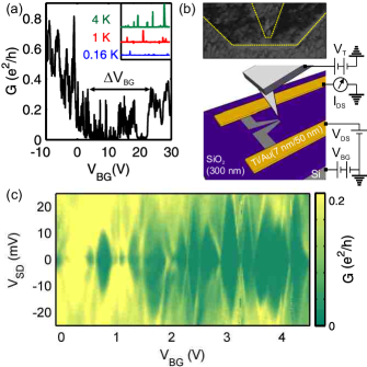
Our graphene flakes are mechanically exfoliated from natural graphite onto a highly doped Si substrate capped with a 300 nm thick SiO2 layer. Optical microscopy [Casiraghi et al., 2007] and Raman spectroscopy [Ferrari et al., 2006] are used to locate and confirm the flakes are monolayers. Two 10/50 nm thick Ti/Au contacts were patterned using lift-off processing and a 90 nm wide channel connected by tapered leads was etched using an O2 plasma [Fig. 1(b).] Figure 1(a) shows the conductance of the device as a function of voltage applied to the Si back-gate at = 8 K. As expected [Stampfer et al., 2009a], is strongly suppressed for a range around the neutrality point (12 V) except for irregularly spaced resonances where increases over a narrow range of . The density of resonances decreases at lower temperature while their lineshape remains roughly constant [inset, Fig. 1(a).] At larger source-drain voltage () the conductance between the resonances increases, leading to =15-20 mV high diamond shaped regions where current is blockaded [Fig. 1(c).]
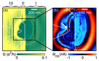
A schematic of our setup used to perform scanning gate microscopy (SGM) is shown in Fig. 1(b). We use a Pt/Ir coated cantilever (NanoWorld ARROW-NCPt) with a nominal tip radius of 15 nm. To perform SGM a current is driven through the device and its conductance is recorded as a function of tip position. Figure 2(a) shows a typical SGM image [Horcas et al., 2007] captured over the constriction in tapping mode with =0.5 V and =0 V. Elongated halos alternating between enhanced and suppressed encircle the constriction. Each halo corresponds to the locus of points where the tip’s contribution to the electrostatic potential is sufficient to overcome the coulomb blockade [Woodside and McEuen, 2002]. The halos are continuous in region I but are broken by a stripe in region II where the tip crosses the outer graphene edge on either side. This stripe rotated with the scan direction and was always parallel to the fast scan axis. A region with these properties was also observed in SGM of subsurface quantum dots [Pioda et al., 2004], where it was attributed to tip-induced rearrangements of charge. Although their elongated axis is still aligned with the channel, in region III the halos are indented where the inside edge of the constriction meets the tapered lead. This indent is highlighted in Fig. 2(b), which shows an SGM image of the transconductance captured under the same conditions as Fig. 2(a), but with a modulated tip bias to enhance the contrast [Connolly et al., 2010]. There is good agreement between the origin of the halos and the topographic location of the constriction, presumably due to the proximity of the tip in tapping mode [Dorn et al., 2004a]. While this mode was useful for relating SGM structures to the underlying topography, it was unsuitable for continuous use as the distribution of resonances in changed between successive scans. To avoid this instability we performed all subsequent scans in “lift-mode” with the static tip 30 nm from the surface, and used the indent [arrow, Fig. 2(b)] as a reference point for overlaying the topographic outline.
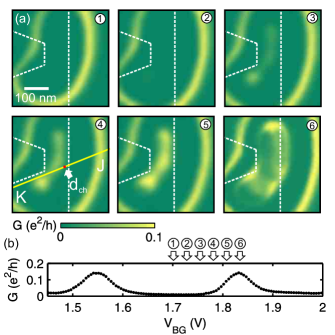
To establish where the conductance haloes originate we park the biased tip (= 2 V) over the channel and tune such that lies between two resonances [Fig. 3(b).] The first resonance manifests as the outer halo in image 1 of Fig. 3(a). With increasing the second resonance emerges as a disordered domain, which is aligned with the channel and extends into the leads with weak and variable contrast [images 2-5, Fig. 3(a)]. Once is tuned to the peak of the second resonance the domain is roughly the same width as the channel and splits into a single halo [image 6, Fig. 3(a).] This observation is in good agreement with recent scanning gate work on similar graphene nanostructures [Dorn et al., 2004a]. The central position of the domain and sensitivity to tapping-mode-induced changes in the electrostatic environment suggest that potential inhomogeneity-, rather than edge roughness-, induced localization is the dominant mechanism in our structure [Ni et al., 2009, Todd et al., 2009]. While the shape of the domain depends on the profile of the tip potential as well as the shape of the region of localized states [Kicin et al., 2005], we assume that tip-induced distortions play less of a role here because the orientation, width, and location of the domain compare favourably with the constriction itself.
While the overlapping coulomb diamonds and a reduction in the density of resonances at lower temperature implies that localization is due to chargeable islands separated by tunnel barriers [Dorn et al., 2004b], our SGM images do not exhibit the characteristic signatures of multiple quantum dots, such as interlocking or anti-crossing halos [Dorn et al., 2004a, Bieszynski et al., 2007, Woodside and McEuen, 2002]. These observations are reconciled in the case of islands with insufficient capacitive coupling to create charging effects between them [Dorn et al., 2004a]. The latter may reflect the elevated tunnel coupling () of the barriers in this region of , an interpretation supported by the independence of the peak lineshape, which suggests . Furthermore, one would expect the effect of a broad tip potential to be similar to a global back-gate if the islands are closely spaced, leading to concentric, rather than interlocking, halos around the domain seen in Fig. 3(a).
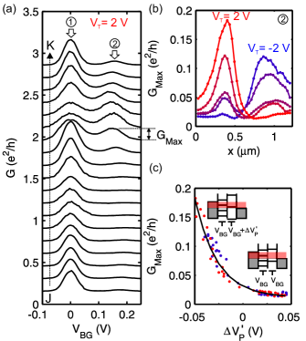
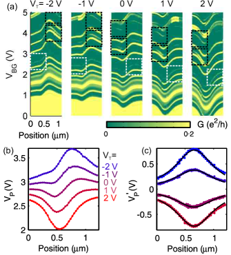
In the absence of pronounced multiple-dot features in the shape of the halos we focus on the tip-position dependent amplitude modulations within the domain of Fig. 3(a). The tip was moved in nm steps along the line in Fig. 3(a) and the back-gate voltage was swept at each point. The resulting maps are plotted in Fig. 4(a) at different tip voltages. Fig. 4(b) shows a typical set of curves, where denotes the position of a resonance in back-gate voltage. By subtracting from each its behaviour at =0 V we obtain a set of corrected data which are symmetrical and well fitted by Lorentzians given by , where is the centre of the Lorentzian along , is its full-width half maximum, and , with 0.38. We find 67510 nm and 80520 nm for thirty six curves corresponding to nine of the resonances in Fig. 4(a). The value of is in good agreement with the width of tip-induced potentials reported previously [Gildemeister et al., 2007, Wilson and Cobden, 2008]. The centre has been indicated in Fig. 3(a). We attribute the variation of at zero to a combination of screening, contact potential difference, charged debris on the tip, and capacitive coupling between the tip and the back-gate [Gildemeister et al., 2007, Kicin et al., 2005, Bieszynski et al., 2007]. Note that the symmetry of in Fig. 4(a) improves in the range of and where the images in Fig. 3(a) were captured, supporting our previous assertion that zero- distortions are minimized.
The maximum conductance of the resonances highlighted by black dashed boxes in Fig. 4(a) is enhanced (suppressed) when the tip is closer to () for =2 V, while the opposite behaviour is observed when = -2 V. Line plots of around the pair of resonances in the middle box are shown in Fig. 5(a), with the tip-induced background variation in removed to facilitate comparison. Since exchanging both the side and sign of the tip potential preserves the in-plane electric field direction, i.e. , the observed asymmetry can be described in terms of the tilted potential induced along . To confirm this, in Fig. 5(b) we plot as a function of , the gradient of the corrected tip-induced potential shown in Fig. 4(b), which is related to the in-plane field by . The data follow the same dependence on for = 2 V, confirming that in this range the tilted potential controls the amplitude of this resonance. The data is well described by an exponential function where 0.01 accounts for the non-zero conductance floor and 0.02 V. Similar behaviour is observed for the resonance in the other black box in Fig. 4(a) and the opposite for the resonance in the white dashed box. Such variations in are usually ascribed to tip-induced modulations in the tunnel barriers, and are therefore compatible with single dot behaviour [Fallahi et al., 2005]. The exponential dependence on is moreover highly suggestive of tunnel barrier suppression. However, in light of the multiple-dot behaviour in the transport data we propose an alternative scenario. The different charging energies and coupling between the back-gate and the dots leads to a random distribution of resonances in as a dot with the weakest coupling to the back-gate modulates the amplitude of resonances from the more strongly coupled dot(s) [Ruzin et al., 1992, Gallagher et al., 2010]. The tilted potential introduced by the tip effectively offsets the ladder of charge states in the dots relative to one another [inset, Fig. 5(c).] As a result the alignment of states in different dots either increases [peak 2 in Fig. 5(a)] or decreases [peak 1 in Fig. 5(a), and resonance in the white dashed box in Fig. 4(a)] depending on their initial detuning. Within this picture, traces the resonance of a weakly coupled dot.
To summarize, we have investigated the response of a graphene nanoconstriction to the local electrostatic potential of a scanning probe tip. Weakly invasive scanning affects the resonance distribution within the transport gap, suggesting that localization in graphene nanostructures is sensitive to the local electrostatic environment. The expansion of a single elongated conductance halo around the constriction implies that the localized states consist of a quantum dot induced by potential inhomogeneities within the channel. Transport data combined with measurements at different tip potentials allow us to identify multiple-dot behaviour by analyzing the effect of the tilted potential on the coupling between localized states.
This work was financially supported by the European GRAND project (ICT/FET). ACF acknowledges funding from the European Research Grant NANOPOTS and the Royal Society.
References
- Geim and Novoselov [2007] A. K. Geim and K. S. Novoselov, Nature Materials 6, 183 (2007).
- Bonaccorso et al. [2010] F. Bonaccorso, Z. Sun, T. Hasan, and A. C. Ferrari, arXiv:1006.4854v1 (2010).
- Guettinger et al. [2010] J. Guettinger, T. Frey, C. Stampfer, T. Ihn, and K. Ensslin, arXiv:1002.3771v1 (2010).
- Molitor et al. [2010] F. Molitor, H. Knowles, S. Droescher, U. Gasser, T. Choi, P. Roulleau, J. Guettinger, A. Jacobsen, C. Stampfer, K. Ensslin, et al., Europhys. Lett. 89, 67005 (2010).
- Buitelaar et al. [2008] M. R. Buitelaar, J. Fransson, A. L. Cantone, C. G. Smith, D. Anderson, A. Ardavan, A. N. Khlobystov, G. W. Morley, K. Porfyrakis, and G. A. D. Briggs, Phys. Rev. B 77, 245439 (2008).
- Ponomarenko et al. [2008] L. A. Ponomarenko, F. Schedin, M. I. Katsnelson, R. Yang, E. W. Hill, K. S. Novoselov, and A. K. Geim, Science 320, 356 (2008).
- Stampfer et al. [2009a] C. Stampfer, J. Guttinger, F. Molitor, D. Graf, T. Ihn, and K. Ensslin, Appl. Phys. Lett. 92, 012102 (2009a).
- Dorn et al. [2004a] A. Dorn, T. Ihn, K. Ensslin, W. Wegscheider, and M. Bichler, Phys. Rev. B 70, 205306 (2004a).
- Stampfer et al. [2009b] C. Stampfer, J. Guttinger, S. Hellmuller, F. Molitor, K. Ensslin, , and T. Ihn, Phys. Rev. Lett. 102, 056403 (2009b).
- Todd et al. [2009] K. Todd, H.-T. Chou, S. Amasha, and D. Goldhaber-Gordon, Nano Letters 9, 416 (2009).
- Chen et al. [2007] Z. Chen, Y. M. Lin, . J. Rooks, and P. Avouris, Physica E 40, 228 (2007).
- Han et al. [2007] M. Y. Han, B. Ozyilmaz, Y. Zhang, and P. Kim, Phys. Rev. Lett 98, 206805 (2007).
- Molitor et al. [2009] F. Molitor, A. Jacobsen, C. Stampfer, J. Guttinger, T. Ihn, and K. Ensslin, Phys. Rev. B 79, 075426 (2009).
- Liu et al. [2009] X. Liu, J. B. Oostinga, A. F. Morpurgo, and L. M. K. Vandersypen, Phys. Rev. B 80, 121407 (2009).
- Han et al. [2010] M. Y. Han, J. C. Brant, and P. Kim, Phys. Rev. Lett 104, 056801 (2010).
- Evaldsson et al. [2008] M. Evaldsson, I. V. Zozoulenko, H. Xu, and T. Heinzel, Phys. Rev. B 78, 161407 (2008).
- Adam et al. [2008] S. Adam, S. Cho, M. S. Fuhrer, and S. D. Sarma, Phys. Rev. Lett. 101, 046404 (2008).
- Sols et al. [2007] F. Sols, F. Guinea, and A. H. C. Neto, Phys. Rev. Lett. 99, 166803 (2007).
- Casiraghi et al. [2007] C. Casiraghi, A. Hartschuh, E. Lidorikis, H. Qian, H. Harutyunyan, T. Gokus, K. S. Novoselov, and A. C. Ferrari, Nano Lett. 7, 2711 (2007).
- Ferrari et al. [2006] A. C. Ferrari, J. C. Meyer, V. Scardaci, C. Casiraghi, M. Lazzeri, F. Mauri, S. Piscanec, D. Jiang, K. Novoselov, S. Roth, et al., Phys. Rev. Lett 97, 187401 (2006).
- Horcas et al. [2007] I. Horcas, R. Fernandez, J. M. Gomez-Rodriguez, J. Colchero, J. Gomez-Herrero, and A. M. Baro, Rev. Sci. Instrum. 78, 013705 (2007).
- Woodside and McEuen [2002] M. T. Woodside and P. L. McEuen, Science 296, 1098 (2002).
- Pioda et al. [2004] A. Pioda, S. Kicin, T. Ihn, M. Sigrist, A. Fuhrer, K. Ensslin, A.Weichselbaum, S. E. Ulloa, M. Reinwald, and W. Wegscheider, Phys. Rev. Lett. 93, 216801 (2004).
- Connolly et al. [2010] M. R. Connolly, K. L. Chiou, C. G. Smith, D. Anderson, G. A. C. Jones, A. Lombardo, A. Fasoli, and A. C. Ferrari, Appl. Phys. Lett. 96, 113501 (2010).
- Ni et al. [2009] Z. H. Ni, T. Yu, Z. Qiang, Y. Y. Wang, L. Liu, C. P. Wong, J. Miao, W. Huang, and Z. X. Shen, ACS Nano 3, 569 (2009).
- Kicin et al. [2005] S. Kicin, A. Pioda, T. Ihn, M. Sigrist, A. Fuhrer, K. Ensslin, M. Reinwald, and W. Wegscheider, New Journal of Physics 185, 1367 (2005).
- Dorn et al. [2004b] A. Dorn, T. Ihn, K. Ensslin, W. Wegscheider, and M. Bichler, Phys. Rev. B 70, 205306 (2004b).
- Bieszynski et al. [2007] A. C. Bieszynski, F. A. Zwanenburg, R. M. . Westerwelt, A. L. Roest, E. P. A. M. Bakkers, and L. P. Kouwenhoven, Nano Letters 7, 2559 (2007).
- Gildemeister et al. [2007] A. E. Gildemeister, T. Ihn, M. Sigrist, K. Ensslin, D. C. Driscoll, and A. C. Gossard, Phys. Rev. B 75, 195338 (2007).
- Wilson and Cobden [2008] N. R. Wilson and D. H. Cobden, Nano Letters 8, 2161 (2008).
- Fallahi et al. [2005] P. Fallahi, A. C. Bleszynski, R. M. Westervelt, J. Huang, J. D. Walls, E. J. Heller, M. Hanson, and A. C. Gossard, Nano Letters 5, 223 (2005).
- Ruzin et al. [1992] I. M. Ruzin, V. Chandrasekhar, E. I. Levin, and L. I. Glazman, Phys. Rev. B 45, 13469 (1992).
- Gallagher et al. [2010] P. Gallagher, K. Todd, and D. Goldhaber-Gordon, Phys. Rev. B 81, 115409 (2010).