Metal-Insulator Transition of the LaAlO3-SrTiO3 Interface Electron System
Abstract
We report on a metal-insulator transition in the LaAlO3-SrTiO3 interface electron system, of which the carrier density is tuned by an electric gate field. Below a critical carrier density ranging from , LaAlO3-SrTiO3 interfaces, forming drain-source channels in field-effect devices are non-ohmic. The differential resistance at zero channel bias diverges within a 2 variation of the carrier density. Above , the conductivity of the ohmic channels has a metal-like temperature dependence, while below conductivity sets in only above a threshold electric field. For a given thickness of the LaAlO3 layer, the conductivity follows a characteristic. The metal-insulator transition is found to be distinct from that of the semiconductor 2D systems.
pacs:
73.23.-b, 73.20.-r, 73.40.-c, 73.43.NqConducting electron systems with unique properties can be generated at interfaces between highly insulating oxides, the most widely studied case being the interface between the TiO2-terminated (001) surface of SrTiO3 and LaAlO3 Ohtomo and Hwang (2004). This electron system behaves as a two-dimensional (2D) electron liquid Breitschaft et al. (2010) for which superconducting Reyren et al. (2007) and magnetic ground states Brinkmann et al. (2007) have been reported. At low temperatures, the interface can be tuned from a superconducting to a resistive state by applying transverse electric fields Caviglia et al. (2008). At higher temperatures, large electric gate fields drive the system through a metal-insulator transition (MIT) Thiel et al. (2006); Cen et al. (2008).
The LaAlO3-SrTiO3 2D system is disordered Thiel et al. (2009); the disorder arising, for example, from dislocations crossing the interface, or from point defects. Consequently, as a 2D electron system (2DES), the interface is expected to be an insulator for , at least for negligible interaction strength among the electrons Abrahams et al. (1979). The observed metallic behavior may be interaction-driven or a crossover effect; sizable interactions have indeed to be anticipated due to the large interaction energy at small carrier densities Li et al. (2010); com (a). Indeed, for the 2DES of semiconductor interfaces Kravchenko et al. (1995); Kravchenko and Sarachik (2004) it has been argued Dobrosavljević et al. (1997) that the metallic phase is not a Fermi liquid because a fictitious electron system with suppressed electronic correlations would form a localized phase Abrahams et al. (1979) rather than a 2D Fermi gas. The polar nature of the LaAlO3-SrTiO3 interface possibly results in additional defects and excitations. Excitations of localized electrons and charged defects, for example, can enhance dephasing and thereby reduce weak localization.
The MIT at semiconductor interfaces is still being debated intensely Popović et al. (1997); Meir (1999); Pastor and Dobrosavljević (1999); Altshuler and Maslov (1999); Washburn et al. (1999); Tracy et al. (2009). The discovery of a MIT at the interface of perovskite oxides, an entirely different host structure for a 2DES, may shed light on the nature of the MIT in two dimensions. In previous experiments Thiel et al. (2006); Cen et al. (2008) the MIT was deduced from the suppression of the conductance, but has not been investigated further.
In field-effect studies of the perovskite interfaces, the gate fields were considered to change the properties of the electron system primarily by altering the carrier density . It has recently been revealed, that by compressing the electron wave function toward the interface, the field also changes the effective disorder of the system and therefore its electronic mobility Bell et al. (2009a).
To advance these issues further, we have measured the current-density vs. electric-field characteristics () of the interface electron system as a function of applied gate fields. These studies show that in the samples investigated the effects of the gate fields have a strong component that arises from a change of . The data furthermore reveal a power-law behavior of the conductivity of the 2D electron liquid as function of .
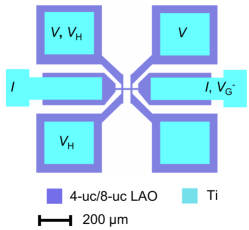
For the measurements we have fabricated seven samples with thicknesses of the LaAlO3 layers of 4 and 8 unit cells (uc) to investigate a possible dependence of the field effects on the LaAlO3 thickness. The thickness of 4 uc was chosen to yield the critical thickness required for interface conduction Thiel et al. (2006). The samples were fabricated by epitaxially growing LaAlO3 layers on the (001) surfaces of TiO2-terminated Kawasaki et al. (1994); Koster et al. (1998), 1 mm thick SrTiO3 single crystals. Scanning force microscopy was used to verify that the substrate surfaces were atomically flat. The films with a nominal composition of LaAlO3 were grown by pulsed laser deposition from a single crystalline LaAlO3 target using standard deposition conditions (780 ∘C, mbar O2). By reflective high energy electron diffraction the thickness of the LaAlO3 layers was controlled with a precision of uc. After growth, the films were annealed for an hour in 400 mbar O2 to minimize oxygen vacancies. The devices were photolithographically patterned Schneider et al. (2006) into the structure shown in Fig. 1. This structure was optimized for Hall measurements and for four-point measurements of the -characteristics, using a small distance between the voltage contacts to minimize the inhomogeneity of the gate fields. Contact pads for the voltage and current leads were prepared by sputtering Ti into holes Ar-ion etched through the LaAlO3. The back gate was provided by silver diffused into the SrTiO3.
For each gate voltage () the -characteristic in zero magnetic field, Hall voltages and the magnetoconductances at several gate voltages were measured. Gate leakage was always below 1 nA. Only negative gate voltages were applied, for these characteristics were found to be reversible with .
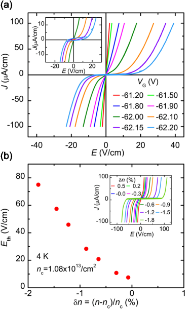
The -characteristics are shown in Fig. 2(a). At small and small ( V, 4 K) the characteristics are linear for the whole range of and for K. At larger ( V, 4 K), however, the -characteristics are nonlinear, showing an enhanced differential resistance for small currents. For V (inset of Fig. 2(a)), the curves show a clear threshold behavior: below a characteristic threshold field , the current density is extremely small ( A/cm) and shows a weak hysteretic behavior, which is caused by the -time constant of the measurement. Because these current densities are minute, we cannot rule out that they are affected by finite gate currents. Above the current grows nonlinearly. The width diminishes with increasing to approach zero at a critical density (Fig. 2(b)) defined below.
The conductivity curves bear the characteristic shape shown in Fig. 3(a) for the 4 uc thick samples in zero magnetic field. The 8 uc thick samples display a similar, but noisier behavior (shown in supplement). For the conductivity at zero bias decreases approximately linearly with . As long as the samples show linear com (b) -characteristics, e.g. at V (Fig. 2(a)), their conductivities are at least of order . Conductivity values with that are plotted in Fig. 3(a) were obtained from non-linear characteristics and present the differential conductivity at zero bias (). For (depending on sample and temperature), however, collapses and the samples are effectively insulating (Fig. 2), unless an in-plane electric field is applied. The transition from the insulating to the linear regime occurs within and is reversible with . The Hall mobility is small near the transition, equalling and as calculated in the linear regime for the 4 and 8 uc thick samples, while outside the transition reaches 1000 cm2/Vs.
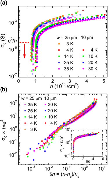
Overall, the temperature dependence of the conductivity is surprisingly weak and can, to a large extent, be absorbed into a simple shift of the curves along the -axis. For all samples of a given thickness we therefore find that the -characteristics in the ohmic regime can be scaled onto a master curve (Fig. 3(b)). In this figure the conductivity is plotted as a function of the reduced carrier density . The values of depend on temperature and are given in the supplementary materials section. For , in this range , the master curve is characterized by a power-law behavior , with . Interestingly, the interfaces follow this characteristic curve for the whole temperature range for which the experiments could be performed (4.2 K K), although the dielectric constant of SrTiO3 is temperature dependent. While the data of the 8 uc samples are characterized by considerably larger scatter, for they approach the curve of the 4 uc thick samples (shown in the supplement).
In the vicinity of the MIT, within a 2 variation of the carrier density, the data scatter more and the zero-bias differential conductivity deviates from a power-law dependence, when . Similarly, on the insulating side a decrease of by just or % causes substantial threshold fields (Fig. 2b).
For an analysis of the behavior close to the MIT, it is suggestive to compare the 2DES of LaAlO3-SrTiO3 interfaces to the 2DES of semiconductor interfaces Kravchenko et al. (1995); Kravchenko and Sarachik (2004); Popović et al. (1997); Washburn et al. (1999), for which many different scenarios have been discussed, see, e.g., Dobrosavljević et al. (1997); Popović et al. (1997); Washburn et al. (1999); Meir (1999); Altshuler and Maslov (1999); Pastor and Dobrosavljević (1999). In these semiconductor systems, the transition is controlled by two parameters, temperature and density, whose interplay can be described by a single-parameter scaling function, , where is the correlation length exponent, and the dynamical critical exponent. These exponents are usually of the order of one. In contrast, the conductivity of the LaAlO3-SrTiO3 interfaces is primarily controlled by ; the temperature has very little influence and accordingly such a scaling relation is not found. In this respect, the MIT is not comparable to that of the semiconductor interfaces. Moreover, the -characteristics for display a threshold behavior with a subsequent dependence which has not been observed for the semiconductor interfaces.
Several candidates of possible insulating states exist. The first candidate is an Anderson insulator, in which single electrons are localized by disorder. The second candidate arises, if Coulomb interactions are strong; the electrons then form a Wigner crystal which is pinned by disorder. The third candidate is a polaronic insulator; strong electron-phonon interaction can lead to a self-trapping and localization. One of our surprising results is the absence of significant temperature dependencies of the -characteristics in combination with strong non-linear effects from moderate electric fields. In a typical electric field of 10 V/cm, an electron has, for example, to travel about 1 m, more than 100 times the typical distance of electrons at , to gain an energy of (for K). The effective absence of thermal effects therefore implies that either barriers prohibiting transport are macroscopic in size or that the motion of electrons is controlled by a collective effect in which many electrons participate as is, e.g., the case in a Wigner crystal. Indeed, the characteristic dependence of the conductivity on the electric field is known from the depinning of two-dimensional vortex lattices in superconducting films Kes and Tsuei (1983). Also simple estimates com (a) suggest that Coulomb interactions can be sufficiently strong to induce Wigner crystallization, especially if one takes into account that polaronic effects may enhance the tendency to crystallization.
A possible scenario is therefore that at the MIT an insulating phase, such as a pinned Wigner crystal, percolates through the system. Remarkably, the MIT has been related to a percolation transition also in semiconductor systems Tracy et al. (2009); Meir (1999). The critical conductance exponent of a percolation transition in 2D is 1.3, in conformity with our findings. For the low electronic densities in the semiconductor systems, the transition is possibly induced through scattering by unscreened impurity charges Tracy et al. (2009). For the LaAlO3-SrTiO3 2D system the charge density of order is so high that it may preclude the observation of a percolation transition driven by unscreened impurity charges. An alternative possibility is a transition where a Wigner crystal or another phase, e.g., a glassy state induced by strong Coulomb interactions Pastor and Dobrosavljević (1999), melts. It is also noted that for oxide materials is a small carrier density. The carrier injection induced by a electric field causes a non-equilibrium state with a carrier density that is locally enhanced. We therefore regard it as a possibility that the MIT is influenced or even triggered by macroscopic inhomogeneities in the sample and the enhanced carrier density at the contacts. This could also affects the -dependencies, causing non-linearities.
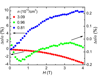
To illustrate the characteristics of the LaAlO3-SrTiO3 interface above the MIT, typical magnetoconductance curves are shown in Fig. 4. At high carrier density, the -characteristics exhibit a dependence (red curve), resembling the typical behavior of metals in small magnetic fields. As revealed in previous studies Bell et al. (2009b); Caviglia et al. (2008); Ben Shalom et al. (2010); Caviglia et al. (2010), the magnetoconductance of the depleted LaAlO3-SrTiO3 interface shows a negative derivative in low fields and a positive in high fields (green curve). This behavior has been interpreted as the result of spin-orbit interaction and weak localization Caviglia et al. (2010). Near the MIT, in contrast, the magnetoconductance is always positive and has a negative second derivative in high fields (blue curve).
In summary, the transport properties of LaAlO3-SrTiO3 interfaces were measured as a function of the mobile carrier density altered by gate fields. It is found that below a critical carrier density the interfaces become insulating for small in-plane electric field. For samples with 4 uc thick LaAlO3 layers, this transition occurs at a conductivity of order . For a wide range of temperatures, the dependencies of the conductivity on the reduced carrier density follow a characteristic.
While it remains to be explored, which of the proposed microscopic mechanisms, such as disorder potentials or polaronic enhancement of Wigner localization, determine the nature of the MIT, it is evident that the MIT in LaAlO3-SrTiO3 interfaces differs qualitatively from the one in two-dimensional semiconductor systems.
Acknowledgements.
The authors gratefully acknowledge fruitful discussions with T. Nattermann and financial support by the DFG (TRR 80, SFB 608) and the EU (oxIDes).References
- Ohtomo and Hwang (2004) A. Ohtomo and H. Hwang, Nature 427, 423 (2004).
- Breitschaft et al. (2010) M. Breitschaft et al., Phys. Rev. B 81, 153414 (2010).
- Reyren et al. (2007) N. Reyren et al., Science 317, 1196 (2007).
- Brinkmann et al. (2007) A. Brinkmann et al., Nat. Mat. 6, 493 (2007).
- Caviglia et al. (2008) A. D. Caviglia et al., Nature 456, 624 (2008).
- Thiel et al. (2006) S. Thiel et al., Science 313, 1942 (2006).
- Cen et al. (2008) C. Cen et al., Nature Materials 7, 298 (2008).
- Thiel et al. (2009) S. Thiel et al., Phys. Rev. Lett. 102, 046809 (2009).
- Abrahams et al. (1979) E. Abrahams et al., Phys. Rev. Lett. 42, 673 (1979).
- Li et al. (2010) L. Li et al., arXiv:1006.2847 (2010).
- com (a) At the LaAlO3-SrTiO3 interface, the Fermi energy equals approximately 10 meV com (c). Below 50 K, the oxide interfaces therefore do not reach the Fermi temperature. The kinetic energy per particle is and the Coulomb interaction , so that . With a dielectric constant we conclude that the Coulomb energy exceeds the kinetic energy by an order of magnitude, similar to the semiconductor systems.
- Kravchenko et al. (1995) S. V. Kravchenko et al., Phys. Rev. B 51, 7038 (1995).
- Kravchenko and Sarachik (2004) S. V. Kravchenko and M. P. Sarachik, Rep. Prog. Phys. 67, 1 (2004).
- Dobrosavljević et al. (1997) V. Dobrosavljević et al., Phys. Rev. Lett. 79, 455 (1997).
- Popović et al. (1997) D. Popović, A. B. Fowler, and S. Washburn, Phys. Rev. Lett. 79, 1543 (1997).
- Meir (1999) Y. Meir, Phys. Rev. Lett. 83, 3506 (1999).
- Pastor and Dobrosavljević (1999) A. A. Pastor and V. Dobrosavljević, Phys. Rev. Lett. 83, 4642 (1999).
- Altshuler and Maslov (1999) B. L. Altshuler and D. L. Maslov, Phys. Rev. Lett. 82, 145 (1999).
- Washburn et al. (1999) S. Washburn et al., Ann. Phys. 8, 569 (1999).
- Tracy et al. (2009) L. A. Tracy et al., Phys. Rev. B 79, 235307 (2009).
- Bell et al. (2009a) C. Bell et al., Phys. Rev. Lett. 103, 226802 (2009a).
- Kawasaki et al. (1994) M. Kawasaki et al., Science 266, 1540 (1994).
- Koster et al. (1998) G. Koster et al., Appl. Phys. Lett. 73, 2920 (1998).
- Schneider et al. (2006) C. W. Schneider et al., Appl. Phys. Lett. 89, 122101 (2006).
- com (b) We use the word “ohmic” following the usage to describe characteristics with a finite conductance at . characteristics in which are called “linear”.
- Kes and Tsuei (1983) P. H. Kes and C. C. Tsuei, Phys. Rev. B 28, 5126 (1983).
- Bell et al. (2009b) C. Bell et al., Appl. Phys. Lett. 94, 222111 (2009b).
- Ben Shalom et al. (2010) M. Ben Shalom et al., Phys. Rev. Lett. 104, 126802 (2010).
- Caviglia et al. (2010) A. D. Caviglia et al., Phys. Rev. Lett. 104, 126803 (2010).
- com (c) This applies for and / 3.