Molecular Beam Epitaxy of LiMnAs
Abstract
We report on the molecular beam epitaxy (MBE) growth of high crystalline quality LiMnAs. The introduction of a group-I alkali metal element Li with flux comparable to fluxes of Mn and As has not caused any apparent damage to the MBE system after as many as fifteen growth cycles performed on the system to date.
pacs:
81.15.Hi, 75.50.Ee, 75.50.PpI Introduction
Molecular beam epitaxy (MBE) has proven to be an unrivaled technology for preparing high quality thin-film crystalline materials and layered heterostructures. While it became a standard growth technique in the field of group-IV, III-V and II-VI semiconductors, no epitaxial growth has been reported until recently Jungwirth:2010 for compound materials containing group-I elements. Yet, materials of this class exhibit a variety of properties of basic science and application interests. These include semiconducting band structure (e.g. LiZnAs, Kuriyama , or LiMnAs, Jungwirth:2010 ) combined with high-temperature antiferromagnetism (e.g. LiMnAs, KMnAs, Bronger:1986 ) or with the predicted ferromagnetism in dilute moment sytems (e.g. LiZnMnAs, Masek:2007_a ), and with structural compatibility to III-V zinc-blend materials Achenbach:1981 ; Jungwirth:2010 .
Materials from the I-Mn-V group were previously synthesized from elements by high temperature reaction Bronger:1986 ; Achenbach:1981 . These materials are powder-like, polycrystalline, and sensitive to air moisture. LiMnAs, which we focus on in this paper, crystallizes in tetragonal space group with lattice parameters Å and , as determined from x-ray diffraction (XRD) measurements Achenbach:1981 . The spin ordering was determined by neutron diffraction to be antiferromagnetic above room temperature Bronger:1986 .
The fact that MBE growth of LiMnAs, as well as of other group-I compounds, has remained a virtually unexplored territory is likely a result of the common prejudice that high concentrations of strongly reactive alkali metals might damage the MBE system. An indication that this may not be the case and the first study of LiMnAs epilayers has been recently presented in Ref. Jungwirth:2010 . While the report Jungwirth:2010 focuses on the semiconducting nature of antiferromagnetic LiMnAs and outlines a general strategy for employing high-temperature antiferromagnetic semiconductors in spintronics, in this paper we provide a more detailed description of the MBE growth of LiMnAs.
II MBE growth
In addition to common sources of arsenic (As4) and manganese, the MBE system (Kryovak) was equipped with an effusion cell containing elemental lithium (in the form of solid Li chunks) in a 5cc pBN crucible. Molecular fluxes of all three cells were determined by the beam-flux monitor, taking into account the respective molecular weights and atomic numbers Parker . During the growth, the stoichiometric ratio of Li, Mn, and As was adjusted, with a slight excess of As. The corresponding cell temperatures and beam-equivalent pressures are summarized in Tab. 1 for the case of the growth rate of m/hour, used in our experiments.
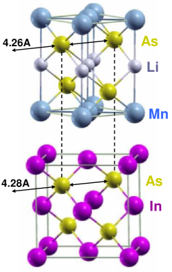
The zinc-blend InAs with the cube lattice parameter 6.06 Å and the tetragonal LiMnAs have identical arrangements in the lattice of the common As planes and the respective As-As bonds are of a very similar length (the difference is 0.4%), as illustrated in Fig.1. Therefore from the lattice matching perspective, InAs(100) is a particularly suitable common substrate material for the epitaxial growth of LiMnAs. The InAs substrate was mounted in the In-free sample holder, heated up to 450∘C for the oxide desorption, and coolled down to the growth temperature of 200∘C (measured by the thermocouple).
| source | C) | BEP (Torr) | |
|---|---|---|---|
| As | 260 | 5.7 | 1.1 |
| Li | 430 | 3.0 | 1.0 |
| Mn | 840 | 1.3 | 1.0 |
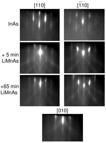
We started the growth of LiMnAs directly on the desorbed InAs substrate surface, without any MBE grown buffer layer. Very quickly after opening the cell shutters a clear, streaky RHEED pattern evolves, showing the (1x1) symmetry of the surface and the 2D growth mode, as ilustrated in Fig. 2. This RHEED pattern remained stable even throughout the longest growth time attempted in our experiments which was three hours, corresponding to the film thickness of m.
The RHEED images of growing LiMnAs are in a striking contrast to those recorded during the growth of a reference MnAs epilayer. If the Li-cell shutter is closed during the growth, under otherwise identical growth conditions, a spotty RHEED pattern quickly emerges which corresponds to the mismatched and poorly growing hexagonal lattice of MnAs Tanaka .
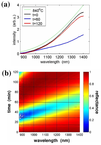
The RHEED growth oscillations were not observed during the growth of LiMnAs. Instead, we calibrated the growth rate ex-situ by measuring (by the Dektak profilometer) the total film thickness across the wafer edges masked during the growth by the sample holder. The reflectance spectroscopy was employed for monitoring the growing LiMnAs layer in-situ. For this purpose we use the radiation which is emitted by the opened hot cells and reflected back by the growing layer. The reflected radiation is recorded by the spectrometer (kSA BandiT, detection range 870-1400 nm) mounted on the central pyrometer port. At the beginning of the growth the detected spectrum closely resembles that of the black-body radiation with temperature close to the temperature of the Mn cell, as shown in Fig. 3(a). During the growth the reflected intensity exhibits clear interference oscillations with the wavelength dependent period. The corresponding time-dependent dimensionless reflectance is shown in Fig. 3(b). The occurrence of Fabry-Perot interference oscillations implies that the growing film is transparent in the detected spectral range.
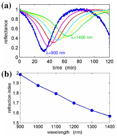
If combined with the known growth rate, the interference period allows us to estimate the index of refraction, as shown in Fig. 4. The resulting value of is relatively low compared to common -band semiconductors. Note that theoretically the low refractive index of LiMnAs is explained by means of the admixture of the correlated Mn -states in the density of states Jungwirth:2010 .
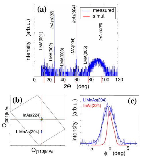
LiMnAs samples of thickness 200 nm were analyzed by XRD. The - scan in Fig. 5(a) shows peaks from the (001) family. Red lines denote the expected bulk positions for LiMnAs(001) reflections which are in a perfect agreement with the observed peaks. The bump at 90∘ may correspond to a small amount of spurious contamination. The epitaxial layer is fully strained, as seen from Fig. 5(b). We verified by -scan around LiMnAs(204) and InAs(224) reflections (see Fig. 5(c)) that the epitaxial relationship is LiMnAs(001)InAs(001) in agreement with the expected relative crystal orientation of LiMnAs grown on InAs (see Fig. 1).
III Conclusions
We have prepared high quality, single crystal thin film samples of LiMnAs by the standard solid source MBE technology which demonstrates the feasibility of epitaxial growth of group-I alkali-metal compounds. The LiMnAs epilayers have the expected crystal structure and epitaxial relationship to the InAs substrate. The materials exhibit an optical gap. Our work opens the possibility for a systematic study of material, optical, electronic, and magnetic characteristics of the family of I-Mn-V antiferromagnetic semiconductors.
Acknowledgments
We greatfully acknowledge helpful assistance of J. Mašek, P. Kužel, B. L. Gallagher, C. T. Foxon, R. P. Campion, and J. Wunderlich. The work was done in the framework of EU Grant FP7-214499 NAMASTE, FP7-215368 SemiSpinNet, from Czech Republic Grants AV0Z10100520, AV0Z10100521, MSM0021620834, MSM0021620857, KAN400100652, LC510, and Preamium Academiae.
References
- (1) T. Jungwirth, V. Novák, X. Martí, M. Cukr, F. Máca, A.B. Shick, J. Mašek, P. Horodyská, P. Němec, V. Holý, J. Zemek, P. Kužel, I. Němec, B.L. Gallagher, R.P. Campion, C.T. Foxon, J. Wunderlich, arXiv:1007.0177v1 (2010)
- (2) K. Kuriyama, T. Kato, K. Kawada, Phys. Rev. B49, 11452 (1994)
- (3) W. Bronger, P. Müller, R. Höppner, H.-U. Schuster, Z. anorg. allg. Chem. 539, 175 (1986)
- (4) J. Mašek, J. Kudrnovský, F. Máca, B.L. Gallagher, R.P. Campion, D.H. Gregory, T. Jungwirth, Phys. Rev. Lett. 98, 067202 (2007)
- (5) G. Achenbach, H.-U. Schuster, Z. anorg. allg. Chem. 475, 9 (1981)
- (6) E.H.C. Parker, The technology and physics of molecular beam epitaxy, Plenum Press (1985)
- (7) M. Tanaka, J.P. Harbison, M.C. Park, Y.S. Park, T. Shin, G.M. Rothberg, J. Appl. Phys. 76, 6278 (1994)