Thermoelectric Properties of Electrostatically Tunable Antidot Lattices
Abstract
We report on the fabrication and characterization of a device which allows the formation of an antidot lattice (ADL) using only electrostatic gating. The antidot potential and Fermi energy of the system can be tuned independently. Well defined commensurability features in magnetoresistance as well as magnetothermopower are obsereved. We show that the thermopower can be used to efficiently map out the potential landscape of the ADL.
A two dimensional electron system (2DES) with a regular array of scatterers is referred to as an antidot lattice (ADL). Over the past two decades, such systems have been studied in great detail revealing a variety of intriguing physical phenomena, ranging from classical pinned orbits in magnetic fields (commensurability) Weiss et al. (1991) to Ahoronov-Bohm type quantum interference effects Schuster et al. (1994). Recently, there has been a renewed interest in ADLs, as it has been shown that they can alter the band structure of a system, resulting in modified optical Pedersen et al. (2008a) and electrical Fürst et al. (2009) properties. ADLs are usually fabricated by the physical removal of material (etching) in the desired region, resulting in a fixed potential profile in the underlying 2DES Weiss et al. (1991). Less destructive techniques such as local oxidation Dorn et al. (2005) or electrostatic gating Lorke et al. (1991) have also been employed in the fabrication of ADLs. However, none of the existing techniques allow for an independent variation of the antidot potential and the Fermi energy of the electron sea between the antidots. The fabrication of such devices with independent tunability of and , would allow for a systematic study of the interplay between these two relevant energy scales. In view of recent proposals for scalable spin-based quantum information processing devices in ADLs Pedersen et al. (2008b); Flindt et al. (2005), this tunability is highly desirable. Furthermore, recent studies in 2D mesoscopic devices in GaAs/AlGaAs heterostructures have revealed the possibility of the existence of spin correlated systems formed due to the existence of intrinsic potential modulations within the 2DES Siegert et al. (2007). Such tunable devices provide the possibility of realizing well-ordered artificial spin-lattices with tunable magnetism in a semiconductor environment.

In this Letter, we describe the properties of ADLs which are induced solely by electrostatic gating. We perform magnetoresistance (MR) and magnetothermopower (MTP) studies to show that and can be controlled independently. We also show that thermopower (TP) is an extremely sensitive tool to study the potential landscape of the ADL system. Silicon -doped GaAs/AlGaAs heterostructures with a nm spacer layer with an as-grown number density of m-2, and low temperature mobility of m2/Vs (corresponding to an elastic mean free path m ) were used in our experiments.
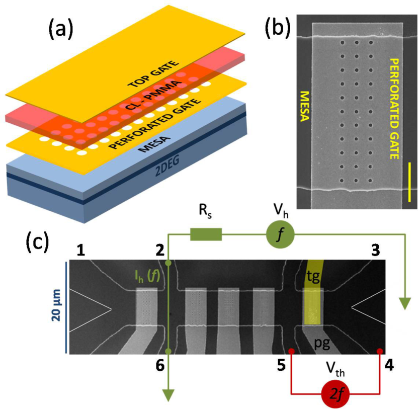
Figure 1(a) shows a schematic of the device structure. Following the definition of a mesa by wet etching, standard electron beam lithography and lift-off techniques were used to obtain a metallic (Ti/Au) perforated gate (PG). The antidot diameter and spacing are fixed by the geometry of the perforations. A nm thick layer of cross-linked polymethyl methacrylate serves as a dielectric between the PG and a Ti/Au top gate (TG). Application of suitable negative voltages on the TG result in the formation of a perfectly periodic ADL in the 2DES. The sheet density, (or ), of the itinerant electrons between the scatterers can be continuously varied by applying voltages to the the PG. Figure 1(b) shows a scanning electron micrograph of one such PG (similar to the ones used in this experiment) prior to deposition of the TG. We were able to reliably fabricate devices with () ranging from nm to nm ( nm to nm).
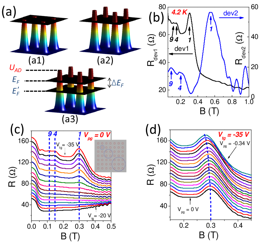
Measurements were performed in a dilution refrigerator with a base temperature of mK. For resistance measurements a current ( A, frequency Hz) was passed between contacts 1 and 3 [Figure 1(c)], and the resultant voltage drop across the device (dev1: nm, nm) was measured between contacts 4 and 5 using a lock-in amplifier yielding the four-probe resistance of the device. Under the influence of a perpendicular magnetic field , electrons move in cyclotron orbits and the cyclotron radius is given by , where is the electron charge. At particular values of , electrons move in pinned orbits around a specific number of antidots resulting in peaks in the resistance whenever is commensurate with the lattice Weiss et al. (1991). Figure 2(b) shows commensurability features for two devices (dev1: nm, nm; dev2: nm, nm) at 4.2 K. was fixed at ( V / V) for (dev1/dev2) with V resulting in the formation of a strong periodic antidot potential in the 2DES not . Clear commensurabilty peaks are observed in both devices corresponding to pinned orbits around (fundamental), and antidots. The higher order peaks ( and ) shift to lower for dev2. This shift has been reported previously for ADLs with a high aspect ratio (i.e., ) Weiss et al. (1991) and is attributed to chaotic electron dynamics Fleischmann et al. (1992). In contrast, we see no such shift for dev1, which has a smaller aspect ratio. We note that dev1 consists of antidots (in a array), which is much lower than typical studies Weiss et al. (1991); Dorn et al. (2005). Despite this, we are able to clearly resolve even higher order commensurability features. This may be due to the fact that the non-destructive (gating) technique used to form the ADL does not severely alter the local electron mobility. For the rest of this work we focus on a detailed study of dev1.
Figure 2(c) shows the variation of low temperature ( mK) MR as a function of . As is reduced (i.e., is increased) from V to V in steps of V (with held at V), we see a clear emergence of commensurability features (for V), which increase in strength as is reduced. This is illustrated schematically in Figure 2(a1 and a2). can be determined from the position of the fundamental commensurability peak ( T), and yields a value of m-2. Alternatively, may be extracted directly from the low- Shubnikov de-Haas (SdH) oscillations resulting in m-2, in excellent agreement with that extracted from the commensurability condition. Using this value of we compute corresponding to the T and T and draw the resultant cyclotron orbits [inset of Figure 2(c)], which confirm that they correspond to orbits around and antidots. We emphasize that the position of the peak is independent of in this range, thus demonstrating that may be continuously varied without any significant effect on of the electron sea. Figure 2(d) shows that at a fixed ( V), can be systematically tuned without affecting . As is varied from V to V [illustrated in Figure 2(a3)], the position of the peak changes continuously from T to T, without a noticeable change in MR profile. This corresponds to a change in from m-2 to m-2 (i.e., meV). Thus, it is clear that and can indeed be controlled independently in our ADL devices.

We now turn our attention to the thermopower (TP) of the ADL. TP is defined as , where is the temperature difference across the system, and is the resultant thermovoltage. TP often yields vital information about energy flow through the system that cannot be gleaned from standard resistance and conductance measurements Appleyard et al. (2000); Scheibner et al. (2005). Various studies in low-dimensional systems have shown that TP is highly sensitive to the local density of states Goswami et al. (2009); Appleyard et al. (2000); Scheibner et al. (2005). However there have been extremely limited studies of TP in ADLs Budantsev et al. (2004); Pogosov et al. (2005). We show that TP is an excellent tool to systematically study ADLs. A schematic of the set-up used for TP measurements is shown in Figure 1(c). A local heating technique is used where a heating current ( A, Hz) flows through one arm of the mesa resulting in a specific across the device. is measured (between contacts 4 and 5) using a lock-in amplifier at . Note that due to the lack of local temperature sensors, the current device geometry does not allow for an accurate measurement of and hence . However, the underlying physics can be explored equally well through a measurement of .

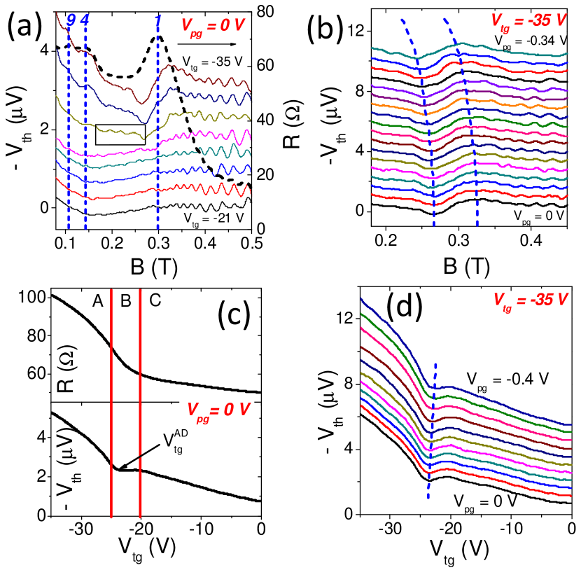
Figure 3(a) shows the variation of MTP with . We find that the signature of commensurability in TP is a sharp change in its magnitude. This can be seen clearly when compared with the peak observed in MR [dashed (black) line in Figure 3(a)]. This is a direct consequence of the Mott formula, appropriately modified for an array of scatterers Pogosov et al. (2002). The qualitative behavior of TP in our device agrees well with that expected from ref. 17 (not shown). As expected, the strength of the feature diminishes when changes from V to V. Figure 3(b) clearly shows a shift in its position when is held constant and is changed from V to V. In addition to the -periodic SdH oscillations, we observe highly reproducible oscillations in TP at low ( T), which are periodic in [boxed region in Figure 3(a)]. Similar oscillations in MR have been reported earlier and have been associated with quantum interference phenomena in ADLs Nihey et al. (1995) or anti-dot charging effects in single antidots Kataoka et al. (1999). Budantsev et al. Budantsev et al. (2004) have observed seemingly similar oscillations in the transverse TP, and attribute them to interference due to electron orbits between four neighboring antidots. However, the observed TP oscillations in our case are associated with electron motion around a single antidot. A detailed analysis of these oscillations will be the subject of another work. We note that these B-periodic oscillations are clearly absent in MR, reinforcing the fact that TP is a more sensitive tool to probe the electronic structure of ADLs.
We now show that the sensitivity of TP can be exploited to directly investigate the interplay between and . Transport through the ADL can be divided into three regimes (A,B and C) [Figure 3(c)]. As is reduced from V to V (region C), the local number density (in the regions determined by the perforations) gradually changes, resulting in an increase in (upper pannel) and (lower pannel). Region B shows a rapid increase in and a sharp dip in . This indicates the onset of strong scattering centers in the 2DES (i.e., the formation of the ADL). In other words, in this region just pierces the Fermi surface [illustrated in Figure 2(a1)], and electrons see an array of scatterers. This picture is corroborated by the fact that commensurability features in MR (and MTP) only become visible when V. For V (region A), sidewise depletion becomes important, resulting in a further increase in TP due to an increase in [illustrated in Figure 2(a2)]. Thus, region B corresponds to a crossover from a situation when the ADL is not defined to one where . The position of the minimum in () may thus be used to identify region B. In this picture, one would expect that should be highly sensitive to . Figure 3(d) shows the variation of with for various . As decreases clearly moves to less negative values, indicating that the ADL is induced at lower values of . The non-monotonic behaviour of TP in region B is a purely electrostatic phenomenon, found to be practically independent of temperature. It may be related to inhomogeneties in resulting from fluctuations in the conduction band due to rapid variations in the impurity potential Siegert et al. (2007). However, a more detailed study is required to confirm its origin. Despite this, we can clearly see that the TP is highly sensitive to the relative magnitudes of and , and can be used to accurately determine the region in which the ADL is formed.
In conclusion, we have demonstrated an ADL device where the antidot potential and Fermi energy of the system can be controlled independently through electrostatic gating. We have characterized the device using resistance and TP measurements and show that TP is a particularly sensitive tool to study the potential landscape in ADLs.
This work was supported by the Department of Science and Technology (Govt. of India), EPSRC (U.K.), and UK-India Educational Research Initiative (UKIERI). S.G. would like to thank the Gates Cambridge Trust for financial support.
References
- Weiss et al. (1991) D. Weiss, M. L. Roukes, A. Menschig, P. Grambow, K. von Klitzing, and G. Weimann, Phys. Rev. Lett. 66, 2790 (1991).
- Schuster et al. (1994) R. Schuster, K. Ensslin, D. Wharam, S. Kühn, J. P. Kotthaus, G. Böhm, W. Klein, G. Tränkle, and G. Weimann, Phys. Rev. B 49, 8510 (1994).
- Pedersen et al. (2008a) T. G. Pedersen, C. Flindt, J. Pedersen, A.-P. Jauho, N. A. Mortensen, and K. Pedersen, Phys. Rev. B 77, 245431 (2008a).
- Fürst et al. (2009) J. A. Fürst, J. G. Pedersen, C. Flindt, N. A. Mortensen, M. Brandbyge, T. G. Pedersen, and A.-P. Jauho, New Journal of Physics 11, 095020 (2009).
- Dorn et al. (2005) A. Dorn, E. Bieri, T. Ihn, K. Ensslin, D. D. Driscoll, and A. C. Gossard, Phys. Rev. B 71, 035343 (2005).
- Lorke et al. (1991) A. Lorke, J. P. Kotthaus, and K. Ploog, Phys. Rev. B 44, 3447 (1991).
- Pedersen et al. (2008b) T. G. Pedersen, C. Flindt, J. Pedersen, N. A. Mortensen, A.-P. Jauho, and K. Pedersen, Phys. Rev. Lett. 100, 136804 (2008b).
- Flindt et al. (2005) C. Flindt, N. A. Mortensen, and A.-P. Jauho, Nano Letters 5, 2515 (2005).
- Siegert et al. (2007) C. Siegert, A. Ghosh, M. Pepper, I. Farrer, and D. A. Ritchie, Nature Phys. 3, 315 (2007).
- (10) is obtained after subtracting a linear background to enhance the clarity of the commensurability features.
- Fleischmann et al. (1992) R. Fleischmann, T. Geisel, and R. Ketzmerick, Phys. Rev. Lett. 68, 1367 (1992).
- Appleyard et al. (2000) N. J. Appleyard, J. T. Nicholls, M. Pepper, W. R. Tribe, M. Y. Simmons, and D. A. Ritchie, Phys. Rev. B 62, R16275 (2000).
- Scheibner et al. (2005) R. Scheibner, H. Buhmann, D. Reuter, M. N. Kiselev, and L. W. Molenkamp, Phys. Rev. Lett. 95, 176602 (2005).
- Goswami et al. (2009) S. Goswami, C. Siegert, M. Baenninger, M. Pepper, I. Farrer, D. A. Ritchie, and A. Ghosh, Phys. Rev. Lett. 103, 026602 (2009).
- Budantsev et al. (2004) M. V. Budantsev, R. A. Lavrov, A. G. Pogosov, A. E. Plotnikov, A. K. Bakarov, A. I. Toropov, D. K. Maude, and J. C. Portal, JETP Lett. 79, 166 (2004).
- Pogosov et al. (2005) A. G. Pogosov, M. V. Budantsev, R. A. Lavrov, A. E. Plotnikov, A. K. Bakarov, and Toropov, JETP Lett. 81, 462 (2005).
- Pogosov et al. (2002) A. G. Pogosov, M. V. Budantsev, D. Uzur, A. Nogaret, A. E. Plotnikov, A. K. Bakarov, and A. I. Toropov, Phys. Rev. B 66, 201303 (2002).
- Nihey et al. (1995) F. Nihey, S. W. Hwang, and K. Nakamura, Phys. Rev. B 51, 4649 (1995).
- Kataoka et al. (1999) M. Kataoka, C. J. B. Ford, G. Faini, D. Mailly, M. Y. Simmons, D. R. Mace, C.-T. Liang, and D. A. Ritchie, Phys. Rev. Lett. 83, 160 (1999).