Urbach tail studies by luminescence filtering in moderately doped bulk InP
Abstract
The shape of the photoluminescence line registered from a side edge of InP wafer is studied as function of the distance from the excitation spot. The observed red shift in the luminescence maximum is well described by radiation filtering and is consistent with the absorption spectra. Our method provides an independent and accurate determination of the Urbach tails in moderately doped semiconductors.
Studies of the optical absorption spectra near the interband absorption edge are widely used for characterization of semiconductor materials. EuSe ; TlGaSe ; GdH3 The spectral dependence at low-energy absorption edge is well approximated by the Urbach exponential decay. Urbach However, the interband absorption usually overlaps with residual absorption by free carriers, masking the true dependence of the absorption tail. In doped samples, the absorption tail is additionally broadened and this effect is also masked by the residual electronic absorption.
Available theoriesGauss ; Lax ; RjJohn ; Greef do not provide description of the interband absorption tailing in the entire energy range from interband to deep tails. Still, they give an insight on the nature of the bandgap fluctuations causing the tailing. Tailing with Gaussian-like asymptotics is characteristic of classical potential fluctuations,Gauss whereas exponential decrease with square-root energy dependence in the exponent is indicative of quantum effects in the band tailing.Lax ; RjJohn Temperature variations of the tailing are accounted for by the adiabatic potential of thermally excited phonons. Greef
In a limited experimental range near the fundamental edge the observed absorption spectra may not differ noticeably from the Urbach law,RjJohn but the temperature and the concentration dependence of the tailing parameters can be very informative. Therefore, accurate studies of the tailing dependence are highly desirable.
In this letter we describe an alternative experimental method for studying the semiconductor absorption edge by measuring the red shift of the peak of the luminescence line, registered from the side edge of the wafer. This shift is sensitive to the sample transparency at the peak wavelength, which is in the region where residual absorption dominates. We show that for moderately doped -InP wafers this technique provides an accurate determination of the Urbach tailing energy.

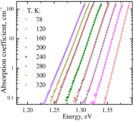
We used 350 m-thick InP wafers, doped -type (S) in the range to cm-3 and measured the reflection and the transmission spectra to evaluate the absorption coefficient .Semyon For all moderately doped samples, cm-3, in the temperature range 78 to 320 K, the absorption edge exhibits an Urbach-type energy dependence in the range to 100 cm-1. For lower doped samples, cm-3, the observed Urbach tail extends deeper into the band gap. One can recover the interband absorption in the bandgap by subtracting the residual (free-carrier) absorption which is essentially constant in this energy region. The resulting red-wing interband absorption spectra are presented in Fig. 1 for a sample with cm-3 at several temperatures. The spectra clearly conform to the Urbach law,
| (1) |
where is the Urbach tail parameter and is the bandgap energy. Matching the values of , well-knownVurgaft for undoped InP, gives cm-1; this value gives a good fit in a wide temperature range to 1000 K.JohnsTielde The physical interpretation of as the value of at (i.e. above the steep slope) suggests that it should not vary with the concentration at a moderate doping level, when the Fermi level is still below the conduction band edge. The experimentally observed temperature variations of and , are proportional to the population of thermally excited phonons and can be estimatedJohnsTielde ; Chung using Einstein’s model for the phonon spectrum. Variations of with the doping concentration reflect the effect of band-gap narrowing combined with Fermi energy shift due to filling of the impurity band,Bugaj while the increase of is attributed to the combined effect of the adiabatic random phonon potential and the random potential produced by concentration fluctuations.Greef

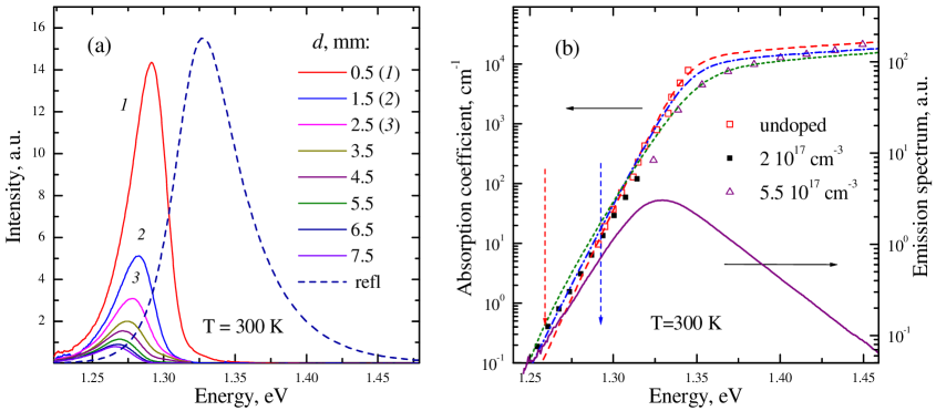
The luminescence spectra were registered from the side edge of the wafer for varying distances between the excitation spot and the edge. The laser excitation energy was chosen close to the absorption edge to ensure large enough excitation volume.Semyon Luminescence spectra for a sample with cm-3 are presented in Fig. 2 (a) for several values of . Also shown (by a dashed line) is the luminescence emission spectrum, as observed in the reflection geometry.Semyon The red shift of the emission line maximum with increasing is clearly seen.
Figure 2 (b) shows the absorption spectraSemyon for several doping levels in a broad energy range that includes the Urbach tail region. Two vertical dashed arrows indicate the range of the luminescence peak positions shown in Fig. 2 (a). Also depicted is the reflection luminescence spectrum on a logarithmic scale ( cm-3, K). It exhibits the exponential decay both in the red and the blue wings, and is well described by the van Roosbroek-Shockley quasi-equilibrium relation, VRSh viz. . Here is an effective temperature that can be estimated from the exponential slope at the blue wing of the spectrum.
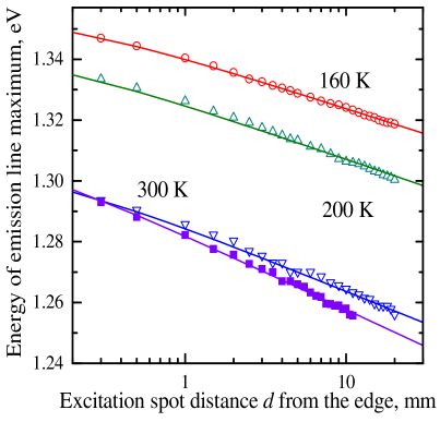
Figure 3 shows the dependence of the luminescence peak position on the distance between the excitation spot and the wafer edge. The observed dependences for several temperatures fit accurately to an expression of the form
| (2) |
where is the Urbach tail parameter and is a small fitting parameter, mm for all samples. The latter reflects details of the experimental geometry (finite width and depth of the excitation spot) and is of no importance for distances in the range of 1 to 20 mm, i.e. for . Taking the values of from the observed dependence , cf. Eq. (1), we find that the only remaining parameter is . This parameter depends on the temperature and doping. Table 1 lists the obtained values of for the sample with cm-3 at several temperatures and also for cm-3 at K.
| , eV | , meV | , meV | |||
|---|---|---|---|---|---|
| 160111 cm-3 | 1.397 | 7.4 | 13 | 0.58 | 0.57 |
| 200111 cm-3 | 1.386 | 7.9 | 14 | 0.54 | 0.56 |
| 300111 cm-3 | 1.355 | 9.4 | 15 | 0.63 | 0.63 |
| 300222 cm-3 | 1.361 | 10.6 | 16 | 0.68 | 0.67 |

Next we show that the observed , including the values of , can be reproduced in a simple model that attributes the luminescent peak shift to wavelength-dependent filtering of outgoing radiation by the sample absorption. We assume that the position of the peak observed at distance from the excitation spot is determined by the transparency of InP wafer to the luminescence spectrum . In other words, the observed spectrum near its maximum should be described by the product . The strong refraction of outgoing radiation and a relatively small observation angle ensure a small and constant range of the angles of incidence. Therefore the dependence of the transparency reflects one-dimensional attenuation of light
| (3) |
The outgoing spectra are not influenced by the surface reflection, but may be modified by multiple interband re-absorption of photons which leads to the creation of new minority carriers and new radiative emission events (photon recycling). However, if the distance is much larger than the width of the minority carrier distribution in the source (including the broadening of this distribution by photon-assisted diffusion), then the spectrum near its peak is quite insensitive to these processes. The maximum of the transmitted spectrum at varying can be found from . Using (3), this equation can be rewritten in the form
| (4) |
To evaluate the left-hand side of Eq. (4), we use the experimental exponential dependence of the luminescence spectra in the red wing. These spectra may be modulated by some factor reflecting the wavelength dependence of the radiation escape probability, but this does not affect the red-wing exponential decay. The intrinsic emission spectrum should be closely similar to the luminescence spectrum measured with high-energy excitation in the reflection geometry, where the observed spectrum is not influenced by the diffusion and filtering effects.
The decay in the red wing below the band edge is of the form
| (5) |
where is another Urbach-like tailing parameter. The experimentally observed values of are listed in Table 1. Using Eqs. (1, 5) to calculate the derivatives in Eq. (4), we find
| (6) |
Comparing Eq. (6) with the empirical dependence (2) gives a physical interpretation to parameter , viz. . As seen from the last two columns of Table 1, this interpretation has excellent agreement with experiment for both samples and all temperatures.
For all studied cases, the values of obtained from the slope of and the slope of the dependence of on are very close, the difference never exceeding 0.2 meV. Thus, the described luminescence method provides an independent way of measuring the tailing parameters. This method can be indispensable (in fact, the only available) in the case when the residual absorption is strong.
In low-doped crystals the Urbach tail is known to be due to the electron-phonon interaction, which implies a certain temperature dependenceUrbach ; JohnsTielde of the tailing parameter . The doping effects in moderately- and highly-doped crystals are more complicated. While grows with doping,Greef the absorption spectrum is at the same time blue-shifted by the Fermi energy of the majority carriers (the Moss-Burstein shift). The smearing of absorption is then modified by the temperature spread of the majority carrier energy distribution. E.g., in doped GaAs samples, the absorption edge is often described by non-Urbach exponential tails of Gaussian type or Halperin-Lax type.Gauss ; Lax These are difficult to distinguish with traditional absorption studies because of the residual absorption. Our evaluation from the luminescence experiments is more accurate in the region of small – allowing to study and identify different types of tailing.
Finally, we note that in moderately doped III-V semiconductors the high quantum radiative efficiency results in high photon recycling Semyon ; Lush2 that gives rise to a photon-enhanced minority carrier transport and can broaden the initial hole distribution over an enlarged diffusion length.Dumke ; vonRoss More accurate considerationSerge10 shows that the recycling-induced carrier transport should be viewed as anomalous diffusion – due to the extremely long photon propagation in the transparency region at the red wing of the emission spectrum. In our experiments, this phenomenon manifests itself as strongly enhanced values of in low-doped samples at K. The approach described in the present work is well suited to study these anomalous diffusion effects, as will be reported separately.
This work was supported by the Domestic Nuclear Detection Office of the Department of Homeland Security, by the Defense Threat Reduction Agency through its basic research program, and by the New York State Office of Science, Technology and Academic Research through the Center for Advanced Sensor Technology at Stony Brook.
References
- (1) R. Akimoto, M. Kobayashi, and T. Suzuki, “The Urbach tail of absorption and photoluminescence spectra in EuSe,” J. Phys.: Cond. Mat. 8, 105 (1996).
- (2) S. Duman and B. Gürbalak, “Urbach tail and optical absorption in layered semiconductor TlGaSe2(1-x)S2x single crystals,” Physica Scripta 72, 79 (2005).
- (3) E. Shalaan and H. Schmitt, “Urbach tail of gadolinium thrihydride films,” J. Matter. Sci. 42, 3255 (2007).
- (4) F. Urbach, “The Long-Wavelength Edge of Photographic Sensitivity and of the Electronic Absorption of Solids,” Phys. Rev. 92, 1324 (1953).
- (5) For a discussion see, e.g., B. I. Shklovskii and A. L. Efros, Electronic properties of doped semiconductors, (Springer, Heidleberg, 1984); further discussion can be found in A. N. Pikhtin and H. H. Hegazy, “Fundamental absorption edge of semiconductor alloys with the direct-gap energy-band structure,” Semiconductors 43, 1259 (2009).
- (6) B. Halperin and M. Lax, “Impurity-Band Tails in the High-Density Limit. I. Minimum Counting Methods,” Phys. Rev. 148, 722 (1966).
- (7) S. John, C. Soukoulis, M. H. Cohen, and E. N. Economou, ”Theory of electron band tails and the Urbach Optical-Absorption Edge,” Phys. Rev. Lett. 57, 1777 (1986).
- (8) C. W. Greeff and H. R. Glyde, “Anomalous Urbach tail in GaAs,” Phys. Rev. B 51, 1778 (1995).
- (9) O. Semyonov, A. V. Subashiev, Z. Chen, and S. Luryi, “Radiation efficiency of heavily doped bulk n-InP semiconductor,” J. Appl. Phys. 108, 013101 (2010), see also http://arxiv.org/abs/1003.6095 .
- (10) I. Vurgaftman, J. R. Meyer, and L. R. Ram-Mohan, “Band parameters for III V compound semiconductors and their alloys,” J. Appl. Phys. 89, 5815 (2001).
- (11) M. Beaudoin, A. J. G. DeVries, S. R. Johnson, H. Laman, and T. Tiedje, “Optical absorption edge of semi-insulating GaAs and InP at high temperatures,” Appl. Phys. Lett. 70, 3540 (1997).
- (12) S. Y. Chung, D. Y. Lin, Y. S. Huang, and K. K. Tiong, “Piezoreflectance study of InP near he absorption edge,” Semicond. Sci. Technol. 11, 1850 (1996).
- (13) M. Bugajski and W. Lewandowski, “Concentration-dependent absorption and photoluminescense of -InP,” J. Appl. Phys. 57, 521 (1985).
- (14) W. van Roosbroek and W. Shockley, “Photon-Radiative Recombination of Electrons and Holes in Germanium,” Phys. Rev. 94, 1558 1954; the relation is also sometimes referred to as the Kubo-Martin-Schwinger theorem, cf. R. Kubo, “Statistical-Mechanical Theory of Irreversible Processes. I. General Theory and Simple Applications to Magnetic and Conduction Problems,” J. Phys. Soc. Jpn. 12, 570 (1957); P. C. Martin and J. Schwinger,“ Theory of Many-Particle Systems,” Phys. Rev. 115, 1342 (1959).
- (15) G. B. Lush,”B-coefficient in n-typeGaAs,” Solar Energy Materials and Solar Cells 93, 1225 (2009).
- (16) P. Dumke, “Spontaneous Radiative Recombination in Semiconductors,” Phys. Rev. 105, 140 (1957).
- (17) O. von Roos, “Influence of radiative recombination on the minority carrier transport in direct band-gap semiconductors,” J. Appl. Phys. 54, 1390 (1983).
- (18) S. Luryi and A. Subashiev, “Semiconductor scintillator for 3-dimensional array of radiation detectors,” in Future Trends in Microelectronics: From Nanophotonics to Sensors to Energy, edited by S. Luryi, J. M. Xu, and A. Zaslavsky (Wiley Interscience, Hoboken, New Jersey, 2010), pp. 331-346, see also http://www.ee.sunysb.edu/~serge/236.pdf .