Present address: ]Fritz-Haber-Institut der Max-Planck-Gesellschaft, Faradayweg 4-6, 14195 Berlin, Germany Present address: ]Department of Physics, University of Illinois at Urbana-Champaign, Urbana, Illinois 61801, USA
We present a first-principles study of the migration and recombination of edge defects (carbon adatom and/or vacancy) and their influence on electrical conductance in zigzag graphene nanoribbons (ZGNRs). It is found that at room temperature, the adatom is quite mobile while the vacancy is almost immobile along the edge of ZGNRs. The recombination of an adatom-vacancy pair leads to a pentagon-heptagon ring defect structure having a lower energy than the perfect edge, implying that such an edge-defect can be formed spontaneously. This edge defect can suppresses the conductance of ZGNRs drastically, which provides some useful hints for understanding the observed semiconducting behavior of the fabricated narrow GNRs.
Spontaneous edge-defect formation and defect-induced conductance suppression in graphene nanoribbons
pacs:
73.22.-f, 61.48.De, 71.15.Mb, 73.63.-bI Introduction
Graphene, a two-dimensional honeycomb lattice of carbon atoms, has been regarded as a new promising material for fundamental studies in condensed matter physics since its successful synthesis in recent years review . Subsequently, graphene nanoribbons (GNRs), a quasi-one-dimensional structure of graphene with varying widths, were fabricated by using several methods including e-beam lithography Chen1 ; Han1 , chemical method Dai , metallic nanoparticle etching Datta1 , and microscope lithography Tapaszto ; Weng . As an electronic material, GNRs were found to have some excellent properties such as simple width-dependent band gaps, high carrier mobility at room-temperature and so on, which make them suitable for device applications in nanoelectronics Chen1 ; Han1 ; Dai ; Son ; Barone1 ; Yan1 ; Beenakker ; Zuanyi1 .
To realize practical applications of GNRs in electronics, their widths must reach true nanometer scale (10 nm), and consequently, edge effects become crucial Tapaszto ; Ritter . Whereas, current GNRs fabricated in experiments inevitably have edge roughness, and their precise atomic edge structures are still unclear and need to be further determined Dai ; Datta1 . Interestingly, recent experiments showed that all sub-10-nm GNRs are semiconducting Dai while previous theoretical works predicted that GNRs with perfect zigzag edges are metallic edge-state . This discrepancy was suggested to originate from complicated edge structures in practice. So far, a lot of theoretical efforts were focused on the electronic structure of edge disorder by using the tight-binding method disorder . In contrast, the evolution and thermodynamics of atomic-scale edge defects have been seldom studied, especially via the first-principles approach. Therefore, exploring possible stable edge defect structures and their influence on the transport properties of GNRs is highly desired and helpful to understand recent experimental observations of GNRs and make use of GNRs in future nanoelectronics.
In this paper, with the density-functional theory (DFT) calculations, we systematically investigate the migration of typical edge defects (carbon adatom and vacancy) and the recombination of the adatom-vacancy pair (AVP) in zigzag GNRs (ZGNRs). We find that an adatom can migrate along the ribbon edge at room temperature while a vacancy cannot. The migration of carbon adatom may lead to the recombination of the AVP and the resulting pentagon-heptagon ring (R57) defect structure is more stable than the perfect edge structure. This localized R57 defect is more likely to exist at the edges of experimentally fabricated ZGNRs than periodic R57 edge structure recently proposed Wassmann1 ; Koskinen1 . We also find that the presence of edge defects causes a decrease in the current through the ZGNR under bias voltage. Especially, for ZGNRs with the R57 edge defect, the current becomes very small and the conductance approaches zero near the Fermi level. This may play an important role in the observed semiconducting behavior of the fabricated narrow GNRs (especially those with zigzag crystallographic edges) Han1 ; Dai ; Tapaszto .
II method and model

Our electronic structure calculations are performed using the Vienna ab initio simulation package (vasp) (Ref. Kresse1, ) within the framework of DFT. The projector augmented wave potential Kresse2 and the generalized gradient approximation with Perdew-Burk-Ernzerhof functional Perdew1 are used to describe the core electrons and the exchange-correlation energy, respectively. The cutoff energy for the plane wave basis set is set to 400 eV. The energies are converged to below eV and the residual forces on all atoms are converged to below 0.01 eV/Å. The minimum-energy path (MEP) calculations for the migration of edge defects have been performed using climbing image nudged elastic band method Henkelman1 . The quantum transport calculations are performed using an ab initio code, atomistix toolkit 2.0 (atk 2.0) Brandbyge1 , which implements non-equilibrium Green’s-function formalism with time-independent DFT DFT-NEGF-LIM . This approach is limited to the steady-state regime and based on a self-consistency procedure. Such limitations makes the approach different from Keldysh’s non-equilibrium Green’s function (see Ref. Stefanucci, ). Since the migration of edge defects are dominated by the atoms nearby, in the calculation of the migration path, we choose ZGNRs with the defect locating at one ribbon edge and the other edge being perfect as the models. To exclude the interaction between defects, we use a supercell including eight unit cells of the ZGNR with the length along the ribbon axis of about 17.95 Å. In the transport calculations, considering that every defect has the same possibility of being located at the two edges in experiments, we choose ZGNRs with both edges having one defect as the models.
III Results and discussion
We start by investigating the stable structures of adatom and vacancy defects at the edge of ZGNRs. As a result of the hybridization in a graphene sheet, each edge atom of a perfect ZGNR has one dangling orbital. When a carbon adatom is located at the ZGNR edge, it prefers to stay at the bridge site between two adjacent edge atoms to form two bonds [the lower panel of Fig. 1(a)]. However, when a vacancy is created at the edge site of the ZGNR by removing an edge carbon atom, the two carbon atoms adjacent to the vacancy, each having one dangling bond, move away a little along opposite directions and form stronger bonds with their adjacent edge atoms [the lower panel of Fig. 1(b)]. And the bond length decreases from 1.38 to 1.25 Å. We further calculate the MEP for the migration of adatom and vacancy defects along the edge of the 7-ZGNR (with seven zigzag chains). The migration barrier () obtained for the edge adatom is 0.76 eV [the upper panel of Fig. 1(a)]. Although -bond breaking and rebonding are involved in this process, the free space in the edge area allows for an easy relaxation of neighboring atoms and substantially lowers the barrier. This barrier is only 0.30 eV higher than the diffusion barrier of a carbon adatom moving over a graphene surface Lehtinen1 . On the other band, the calculated migration barrier of the vacancy is about 2.12 eV [the upper part of Fig. 1(b)], over three times of the barrier of carbon adatom, suggesting that the edge vacancy is much less mobile than the adatom.
In a thermodynamic sense, the rate coefficient for the migration of edge defects is expressed as , where the attempt frequency = can be calculated using the van’t Hoff-Arrhenius law within the harmonic approximation Vineyard1 ; Lee1 . Herein and are, respectively, the normal-mode frequencies at the initial and transition states, and can be obtained from the phonon frequency calculation at each configuration. The calculated attempt frequency, , of the vacancy migration ( s-1) is higher than that of the carbon adatom ( s-1). This is because the bonding between the edge atom and its adjacent atoms is stronger than that between the adatom and its adjacent atoms, leading to a higher vibrational frequency (Note: the migration of the vacancy can be viewed as the migration of the carbon edge atom). The calculated rate coefficient of the adatom migration ( s-1 ) is much larger than that of the vacancy migration ( s-1) at room temperature ( K). This clearly demonstrates that the carbon adatom is quite mobile but the vacancy is almost immobile, consistent with the experimental observation that adatoms are generally much more mobile in the bulk or at the surface than vacancies Banhart1 .
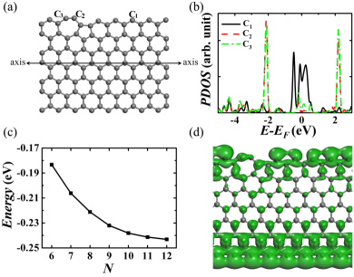
It should be noted that the edge adatoms and vacancies may recombine during their migration, which results in the formation of a stable edge structure. Without loss of generality, we consider the recombination process of the adatom-vacancy pair where an adatom and a vacancy are adjacent to each other. Figure 1(c) shows the MEP of the recombination, as well as the initial structure (AVP) and final structure (perfect edges). It can be seen that the 7-ZGNR with AVP is about 1.90 eV higher in energy than that with perfect edges. The MEP of the recombination is quite complicated, compared with those of migrations of the adatom and vacancy. Interestingly, it is found from the MEP that there exists a structure more stable (about 0.21 eV lower in energy) than the 7-ZGNR with perfect edges. Figure 2(a) shows the detailed structure corresponding to the minimum total energy in the MEP, with one R57 defect at the edge. This result is somewhat unexpected since for perfect carbon nanotubes (CNTs) or graphene, the introduction of the Stone-Wales defect (two pairs of R57) will always increase the total energy of CNTs or graphene Zhou1 ; Crespi1 . Two very recent works have predicted that graphene could have periodic R57 edge structure Wassmann1 ; Koskinen1 , which supports our result to some extent. However, the difference is that the R57 found here is not periodic and is formed from the recombination of the adatom and vacancy. Note that edge adatoms and vacancies can occur with high probability when ZGNRs are prepared in experiments. Thus, in the case of no hydrogenation of edges, local R57 structures are very likely to appear in practice as the adatoms migrate along the edge and the recombination of the adatom and vacancy proceeds.
As shown in Fig. 1(c), the energy barrier of the recombination (i.e., from the AVP to R57 edge structure) is about 0.89 eV Barrier-check1 . The calculated rate coefficient is 0.1 s-1 at room temperature, fast enough to be observed in experimental time scale. Importantly, our further calculations indicate that the barrier and the rate coefficient are insensitive to the widths of ZGNRs. It is thus highly possible to form a R57 structure from the AVP at the edges of ZGNRs. In fact, two very recent experiments have already demonstrated that the migration or vaporization of carbon edge atoms plays an important role of edge reconstruction of graphene and GNRsJia1 ; Girit1 . Especially, the pentagon-heptagon ring can be clearly identified at the zigzag edge in transmission electron microscope images of graphene [see the supporting materials of Ref. Girit1, and Fig. 1 of Ref. Koskinen, ], which supports our theoretical prediction of the stable R57 edge defect. On the other hand, we should note that although the perfect zigzag edge is less stable than the R57 edge structure in energy, the energy barrier of the transformation from the perfect zigzag edge to the R57 structure is quite high [ 1.61 eV as shown in Fig. 1(c)], and the corresponding rate coefficient is small ( s-1 at room temperature). This means that once the perfect zigzag edges are formed, they are relatively stable and will not transform to the R57 edge structure at room temperature for a long time. Such a feature is just consistent with the recent microscopy observations of the perfect zigzag edges appearing under special experimental conditions Jia1 ; Girit1 .
The high stability of the R57 edge, superior to the perfect edge, can be well understood by the formation of new bonds between edge atoms. Compared with 7-ZGNR with perfect edges, two edge atoms in the R57 structure [i.e., and in Fig. 2(a)] can form an additional bond since both of them have the dangling orbitals. This can be clearly seen from two sharp peaks (representing bonding and anti-bonding states, respectively) in the projected density of states (PDOS) of such two atoms [Fig. 2(b)]. The calculated bond length is about 1.23 Å, typical for CC triple bond, which is consistent with the result of the periodic R57 structure Wassmann1 ; Koskinen1 . Therefore, the decrease in energy of the R57 edge structure reflects a compromise between the decrease in the total energy as a result of the formation of new bonds and the increase in energy due to the structural deformation of R57. In addition, our calculations show that the R57 structure can also exist at the open end of zigzag CNTs. For example, the total energy of open-ended (10,0) zigzag CNT with one R57 edge structure is 0.15 eV lower than that with perfect edge structure. Moreover, the energy difference between the ZGNRs with one R57 edge structure and with perfect edges monotonously decreases with the ribbon width [as shown in Fig. 2(c)]: the wider the ZGNR is, the more stable the R57 edge structure is LDA . This is because the stress induced by structural deformation can be released more easily as the width of ZGNRs increases. Typically, the energy difference is about eV per R57 defect for the 12-ZGNR (about 2.4 nm wide).
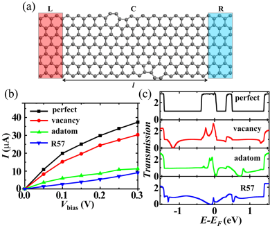
For ZGNRs with perfect edges, two partially flat bands around the Fermi level, which come from / electrons and are mostly localized at the two edges for large wave vector (i.e., edge states), are responsible for the electron transmission under low bias voltages () Zuanyi1 . The presence of edge defects will change the / state and profoundly influence the conduction mechanism Martins1 . To understand the role of edge defects in the transport behaviors of ZGNRs under bias voltages, we carry out extensive first-principle calculations of - curves by using a two-probe system [Fig. 3(a)], where left (L) and right (R) leads are semi-infinite ZGNRs, and the central region (C) is a 7-ZGNR of 14 unit cell length with two edge defects (one at each edge). As shown in Fig. 3(b), the current () of the ZGNR with perfect edges increases rapidly as bias voltage increases, because there are at least one conductance quantum (arising from the / state) around the Fermi level (extra 2 arises from dangling bond states of edge atoms) [Fig. 3(c)]. The presence of any one kind of edge defects, however, always leads to a decrease in the current. For example, for =0.1 V, the currents of 7-ZGNRs with vacancy, adatom and R57 edge defects are 15.26 A, 5.98 A and 2.69 A respectively, which are all smaller than the current of 19.93 A for the 7-ZGNR with perfect edges. More importantly, the current of the ribbon with the R57 defects drops drastically and the system even deviates from original metallic transport behavior of ZGNRs. This can be understood from the transmission spectrum (i.e., quantum conductance) of the 7-ZGNR under a certain bias voltage. As shown in Fig. 3(c), the transmission around the Fermi level for the R57 edge defect is much smaller than that for other cases. As mentioned before, the transport behavior of ZGNRs under low bias voltages is determined by the / state related to the edge states. Among three kinds of edge defects we discuss here, R57 edge defect destroys original hexagonal structure along the edges most seriously, and thus changes the original property of the / state notably [as shown in Fig. 2(d)], and causes a remarkable conductance suppression around the Fermi level.
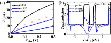
We also calculate the - curve and transmission spectrum for the 7-ZGNR containing only one R57 defect. The results are shown in comparison with those for the ribbons with two perfect edges and with two defective edges in Fig. 4. Under low bias voltages, the current of 7-ZGNR with one R57 edge defect is between those of 7-ZGNR with perfect edges and 7-ZGNR with two R57 defects at both edges, but a little less than their average value. This indicates that the R57 edge defect can significantly reduce the conductance along the defective edge, but the conduction channel along the perfect edge without R57 defect is less affected even for narrow ribbons. The conduction characteristic can be understood from the transmission spectra (i.e., quantum conductance) of the 7-ZGNRs with three kinds of edges mentioned above. Under the same bias voltage, the conductance around the Fermi level of 7-ZGNR with one R57 edge defect is smaller than that with perfect edges, but larger than that with two R57 defective edges. These results further verify the validity of our conclusion that the conductance is drastically suppressed by R57 edge defects in ZGNRs. Moreover, similar transport behaviors are also observed for 11-ZGNRs and fully H-passivated 7-ZGNRs with different defective edges (data not shown). These results confirm a drastic conductance suppression by R57 edge defects in ZGNRs.
Recent experiments showed that all narrow GNRs (from sub-10 nm to several tens nanometer) by lithographical fabrication or chemical growth are semiconductors without evident crystallographic directional dependence Han1 ; Dai ; Tapaszto , while numerous theoretical works predicted all perfect ZGNRs are metallicedge-state . This implies a crucial role of the detailed edge structure in the transport properties of GNRs. In fact, under current experimental techniques, it is still very difficult to obtain GNRs with atomically smooth edges. Thus, our transport calculations based on the used model cannot lead to a direct comparison with present experimental measurements of GNRs, where the edge disorder is generally believed to play a key role in the transport characteristic of GNRs. Considering its high stability, however, we expect that the R57 edge defect may also be an important factor to determine the practical transport behavior of fabricated GNRs. Further studies on other kinds of edge defects as well as edge defect complexes are still needed to fully understand the overall effect of edge defects on the transport properties of GNRs.
IV Conclusions
In summary, we have presented a detailed study on the migration of edge defects (adatom and vacancy) and the recombination of atom-vacancy pair in ZGNRs. The migration barriers of adatom and vacancy are 0.76 eV and 2.12 eV, respectively. The recombination process of the adatom-vacancy pair through the adatom migration, which could occur at room temperature by overcoming an activation barrier of 0.89 eV, will produce a more stable R57 edge structure. It indicates that the ideal ZGNR is less stable than the formed edge-defect structure. The current of ZGNRs with R57 edge defects drops drastically as a result of the notable suppression of conductance around the Fermi level. Our results, indicating a possible stable edge defect structure in experimentally fabricated ZGNRs, provide an explicit mechanism (in addition to the edge disorder) to understand why all narrow GNRs prepared in experiments are semiconductors.
ACKNOWLEDGMENTS
We acknowledge the support of the Ministry of Science and Technology of China (Grant No. 2006CB605105 and 2006CB0L0601), the National Natural Science Foundation of China (Grant No. 10674077), and the A3 Foresight Program of KOSEF-NSFC-JSPS. J.I. was supported by the SRC program of MEST (Center for Nanotubes and Nanostructured Composites).
References
- (1) M. I. Katsnelson, Mater. Today 10, 20 (2007); A. K. Geim and K. S. Novoselov, Nature Mater. 6, 183 (2007); A. H. Castro Neto, F. Guinea, N. M. R. Peres, K. S. Novoselov, and A. K. Geim, Rev. Mod. Phys. 81, 109 (2009); and references therein.
- (2) Z. Chen, Y. Lin, M. J. Rooks, and P. Avouris, Physica E (Amsterdam) 40, 228 (2007).
- (3) M. Y. Han, B. Ozyilmaz, Y. Zhang, and P. Kim, Phys. Rev. Lett. 98, 206805 (2007).
- (4) X. Li, X. Wang, L. Zhang, S. Lee, and H. Dai, Science 319, 1229 (2008); X. Wang, Y. Ouyang, X. Li, H. Wang, J. Guo, and H. Dai, Phys. Rev. Lett. 100, 206803 (2008).
- (5) S. S. Datta, D. R. Strachan, S. M. Khamis, and A. T. Charlie Johnson, Nano Lett. 8, 1912 (2008).
- (6) L. Tapasztó, G. Dobrik, P. Lambin, and L. P. Biró, Nat. Nanotechnol. 3, 397 (2008).
- (7) L. Weng, L. Zhang, Y. P. Chen, and L. P. Rokhinson, Appl. Phys. Lett. 93, 093107 (2008).
- (8) Y.-W. Son, M. L. Cohen, and S. G. Louie, Nature (London) 444, 347 (2006); Phys. Rev. Lett. 97, 216803 (2006).
- (9) V. Barone, O. Hod, and G. E. Scuseria, Nano Lett. 6, 2748 (2006).
- (10) Q. Yan, B. Huang, J. Yu, F. Zheng, J. Zang, J. Wu, B.-L. Gu, F. Liu, and W. H. Duan, Nano Lett. 7, 1469 (2007); B. Huang, F. Liu, J. Wu, B.-L. Gu, and W. H. Duan, Phys. Rev. B 77, 153411 (2008).
- (11) A. Rycerz, J. Tworzydło, and C. W. J. Beenakker, Nat. Phys. 3, 172 (2007).
- (12) Z. Li, H. Y. Qian, J. Wu, B.-L. Gu, and W. H. Duan, Phys. Rev. Lett. 100, 206802 (2008).
- (13) K. A. Ritter and J. W. Lyding, Nature Mater. 8, 235 (2009).
- (14) K. Nakada, M. Fujita, G. Dresselhaus, and M. S. Dresselhaus, Phys. Rev. B 54, 17954 (1996); Y. Miyamoto, K. Nakada, and M. Fujita, ibid. 59, 9858 (1999).
- (15) Y. Yoon and J. Guo, Appl. Phys. Lett. 91, 073103 (2007); D. Basu, M. J. Gilbert, L. F. Register, S. K. Banerjee, and A. H. MacDonald, ibid. 92, 042114 (2008); D. Gunlycke, D. A. Areshkin, C. T. White, ibid. 90, 142104 (2007); A. Lherbier, B. Biel, Y.-M. Niquet, and S. Roche, Phys. Rev. Lett. 100, 036803 (2008); T. C. Li, and S.-P. Lu, Phys. Rev. B 77, 085408 (2008); M. Evaldsson, I. V. Zozoulenko, H. Xu, and T. Heinzel, ibid. 78, 161407(R) (2008); B. Huang, M. Liu, N. Su, J. Wu, W. Duan, B.-L. Gu, and F. Liu, Phys. Rev. Lett. 102, 166404 (2009); E. R. Mucciolo, A. H. Castro Neto, and C. H. Lewenkopf, Phys. Rev. B 79, 075407 (2009).
- (16) T. Wassmann, A. P. Seitsonen, A. M. Saitta, M. Lazzeri, and F. Mauri, Phys. Rev. Lett. 101, 096402 (2008).
- (17) P. Koskinen, S. Malola, and H. Häkkinen, Phys. Rev. Lett. 101, 115502 (2008).
- (18) G. Kresse and J. Furthmüller, Phys. Rev. B 54, 11169 (1996).
- (19) G. Kresse and D. Joubert, Phys. Rev. B 59, 1758 (1999).
- (20) J. P. Perdew, K. Burke, and M. Ernzerhof, Phys. Rev. Lett. 77, 3865 (1996).
- (21) G. Henkelman, B. P. Uberuaga, and H. Jónsson, J. Chem. Phys. 113, 9901 (2000).
- (22) M. Brandbyge, J. L. Mozos, P. Ordejón, J. Taylor, and K. Stokbro, Phys. Rev. B 65, 165401 (2002).
- (23) It should be noted that using electronic structures calculated with density-functional theory for transport calculations might lead to unreliable results for some systems, F. Evers and K. Burke, in Nano and Molecular Electronics Handbook, edited by S. E. Lyshevski (CRC Press, Cleveland/Boca Raton, 2007), p. 24-1. For example, this mean fieldlike, one-electron approach is not able to describe pronounced many-body effects which may appear in some transport processes.
- (24) G. Stefanucci and C.-O. Almbladh, Phys. Rev. B 69, 195318 (2004); G. Stefanucci, S. Kurth, E. K. U. Gross and A. Rubio, in Molecular and Nano Electronics: Analysis, Design and Simulation, Elsevier Series on Theoretical and Computational Chemistry Vol. 17, edited by J. Seminario (Elsevier, New York, 2007), p. 247.
- (25) P. O. Lehtinen, A. S. Foster, A. Ayuela, A. Krasheninnikov, K. Nordlund, and R. M. Nieminen, Phys. Rev. Lett. 91, 017202 (2003).
- (26) G. H. Vineyard, J. Phys. Chem. Solids 3, 121 (1957).
- (27) H. Lee, J. Li, G. Zhou, W. H. Duan, G. Kim and J. Ihm, Phys. Rev. B 77, 235101 (2008).
- (28) F. Banhart, Rep. Prog. Phys. 62, 1181 (1999).
- (29) L. G. Zhou and S. Shi, Appl. Phys. Lett. 83, 1222 (2003).
- (30) V. H. Crespi, M. L. Cohen, and A. Rubio, Phys. Rev. Lett. 79, 2093 (1997).
- (31) To check the validity of our model used, we do complementary energetics calculations for 7-ZGNR with two defective edges. The obtained recombination barrier of an AVP pair is almost the same as that of the 7-ZGNR with one perfect edge and the defect being located on the other edge.
- (32) X. Jia, M. Hofmann, V. Meunier, B. G. Sumpter, J. Campos-Delgado, J. M. Romo-Herrera, H. Son, Y.-P. Hsieh, A. Reina, J. Kong, M. Terrones and M. S. Dresselhaus, Science 323, 1701 (2009).
- (33) Ç. Ö. Girit, J. C. Meyer, R. Erni, M. D. Rossell, C. Kisielowski, L. Yang, C.-H. Park, M. F. Crommie, M. L. Cohen, S. G. Louie and A. Zettl, Science 323, 1705 (2009).
- (34) P. Koskinen, S. Malola, and H. Häkkinen, Phys. Rev. B 80, 073401 (2009).
- (35) Comparative calculations using local-density approximation of the Ceperley-Alder form, D. M. Ceperley and B. J. Alder, Phys. Rev. Lett. 45, 566 (1980), show similar monotonous decrease in the energy difference with increasing ribbon width.
- (36) T. B. Martins, R. H. Miwa, A. J. R. da Silva, and A. Fazzio, Phys. Rev. Lett. 98, 196803 (2007).