Positive and negative Coulomb drag in vertically-integrated one-dimensional quantum wires
Electron interactions in and between wires become increasingly complex and important as circuits are scaled to nanometre sizes, or employ reduced-dimensional conductors Screening like carbon nanotubes cnt1 ; cnt4 ; cnt-proxy1 ; cnt-proxy2 ; cnt-proxy3 , nanowires nanowires1 ; nanowires3 ; surface_effects2 ; nanowires-proxy2 and gated high mobility 2D electron systems Debray ; Yamamoto ; Ed1 . This is because the screening of the long-range Coulomb potential of individual carriers is weakened in these systems, which can lead to phenomenon such as Coulomb drag: a current in one wire induces a voltage in a second wire through Coulomb interactions alone. Previous experiments have observed electron drag in wires separated by a soft electrostatic barrier 80 nm Yamamoto . Here, we measure both positive and negative drag between adjacent vertical quantum wires that are separated by 15 nm and have independent contacts, which allows their electron densities to be tuned independently. We map out the drag signal versus the number of electron subbands occupied in each wire, and interpret the results in terms of momentum-transfer and charge-fluctuation induced transport models. For wires of significantly different subband occupancies, the positive drag effect can be as large as .
Our report addresses the fundamental issues as to what one might expect when coupling quantum circuits in close proximity at the nanoscale. As the transport channel size is reduced towards the one-dimensional limit, charge flow across the channel becomes increasingly dominated by quantum processes. Due to the long-range nature of the Coulomb potential, coupling two quantum circuits in close proximity (separated by a hard barrier of width ) may have profound effects on the current flow and on the equilibrium charge distribution in one wire when current is driven in another wire. First, when is only a few nanometres, tunneling may occur between the two circuits and induce a current. This tunneling current is strongly suppressed with increasing . Even after tunneling becomes negligible, a non-zero potential across one circuit may appear when current flows in the second circuit as a result of Coulomb interactions. This resulting ‘drag signal’ depends critically on the inter-circuit separation, the electronic wire density, and electron-electron interactions in the wire. We have fabricated a device that allows for a large degree of electrical control and tunability between two one-dimensional (1D) quantum circuits, thereby providing us with the platform to study in detail the Coulomb drag signal emanating between two quantum wires separated by only a few tens of nanometre.
The ability to independently control the density of each component in a quantum circuit is an important asset needed to thoroughly characterize the interactions between closely spaced low-dimensional structures. Designs allowing such independent characterization have successfully been implemented in electron-electron Gramilda , hole-hole Jorger and electron-hole Seamons bilayer systems and have led to a great understanding of the interaction mechanisms in two dimensions. Several experiments have been realized in strongly coupled one-dimensional systems consisting of carbon nanotubes cnt-proxy1 ; cnt-proxy2 ; cnt-proxy3 , nanowires nanowires3 ; nanowires-proxy2 or quantum wires networks coupled vertically Auslaender2 ; Ed1 ; Pepper or laterally Debray ; Yamamoto . However, with the exception of laterally coupled quantum wires, none of these one-dimensional networks have been realized with independent electrical contacts and independently tunable density allowing for the measurement of each system component. This is in contrast to our vertically-coupled electrical design where each wire has its own ohmic contacts and capacitively coupled gates.
There are two distinct approaches that can be taken when designing quantum wires coupled by proximity. The first approach is to couple the wires laterally using an electrostatic gate to separate both circuits. Such design allows fabrication of a quantum structures with independent contacts and tunable density, as first demonstrated by Debray et al. Debray , and subsequently by Yamamoto et al.Yamamoto The depth of 2D systems in GaAs heterostructures (typically 80 nm or greater) and the fringing fields of surface defined gates impose that the effective barrier between lateral one-dimensional circuits are soft and are no less than 80 nm. Thus, in order to construct coupled circuits in the 10 nm range, one must couple the circuits vertically. In this design, a hard barrier is introduced during the material growth process, allowing coupling electrical circuits over distances of only a few nanometres. The price to pay in this approach is the complex fabrication process EBASE required for defining quantum wires with independent electrical contacts, as sketched in Fig. 1a-d.
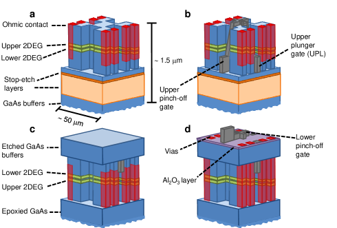
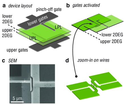
Fig. 2a shows a schematic of the interacting region of such a device. This design was modified from previous work Ed1 so as to enable the measurement of both wires individually, simultaneously and independently. Applying a suitable voltage on the gates selectively depletes the two-dimensional electron gases (2DEGs) such that two independently contacted quantum wires are created, as shown in Fig. 2b and Fig. 2d. In this regime, only 1D regions are vertically coupled and parasitic 2D coupling is minimized. A scanning electron microscope picture of the device is shown in Fig. 2c where long and wide wires are observed. It is important for the alignment between the upper and the lower gates to be lesser than, or equal to 30 nm in the direction perpendicular to the wires to ensure a sub 50 nm effective center-to-center distance between the wires. For the device presented here, this alignment error was less than 25 nm, leading to an effective center-to-center distance between the wires bounded between 33 nm and 41 nm. Finally, the accuracy of the alignment in the direction parallel to the wires is not as crucial as it only affects the 1D-1D interacting length, which is determined to be 2.8 long in this device.
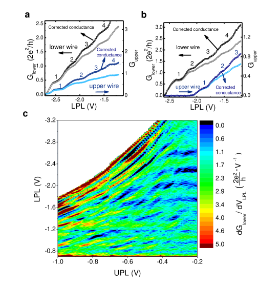
Fig. 3 shows the evolution of the conductance at a temperature of K in each quantum wire as a function of gate voltage. Fig. 3a was taken at a fixed UPL = -0.23 V where both wires have almost identical 1D subband occupancies for a given LPL voltage. For a fixed UPL = -0.34 V, the wires subband occupancies differ greatly, as depicted in Fig. 3b. These measurements demonstrate that our design allows control of the number of occupied subbands in each circuit.
In the ballistic regime, electron transmission is unhindered and in the quantum transport conductance , while an increase in scattering along the wire causes in the non-ballistic regime. The wires presented here are in the non-ballistic regime and the spacing between the conductance plateau features is less than . Correcting for the contact resistance by subtracting a series resistance to the quantum wires yields an even conductance spacing between the plateau-like features, albeit one smaller than , as shown in Fig. 3a and 3b. A 1.25 k (5.00 k) contact resistance was subtracted from the lower (upper) wire conductance. This higher value of the contact resistance is due to partial depletion of the upper 2DEG when the gates are biased for the drag measurement (see Methods). An even conductance spacing of plateau-like features at values lower than in quasi one-dimensional structures was previously observed Yacobywire2 and has been found not to affect the 1D nature of the quantum wires. We also show in Fig 3c the derivative of the conductance of the lower wire as a function of LPL voltage. Plateau-like features are observed when the derivative approaches zero, appearing as black and blue stripes in this mapping. This tracking of the plateau-like features, combined with their even conductance spacing, strongly supports the existence of well-defined one-dimensional subbands.
Coupling two independent electrical circuits by proximity may lead to signals in one circuit whose origin emanates entirely from the neighboring circuit such as Coulomb drag. To measure this drag effect, a current is set in one of the (drive) circuits. Under the condition of no current flow, a voltage develops across the second (drag) circuit, defining a drag resistance that is a direct probe of electron-electron interactions. Coulomb drag is distinct from rectification and ratchets mechanisms where a voltage develops due to a neighboring current flow whose I-V characteristics are highly non-linear (with respect to ) and non-symmetric with respect to probe inversion. In contrast, Coulomb drag is an equilibrium phenomena that is linear, invertible with respect to probe symmetry, mutual, and present in ballistic and non-ballistic circuits.
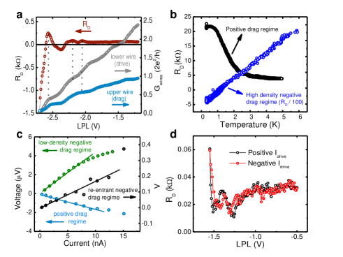
The drag resistance measured in our quantum circuit is shown in Fig. 4a, along with the conductance of each wire. Coulomb drag peaks are observed concomitant with the opening of 1D subbands in either wire (see dotted lines in Fig. 4a). Momentum matching between both wires can explain the presence of the positive drag peaks when the wires have similar subband occupancies Debray , but an enhancement of the electron-hole asymmetry as 1D channels open in the quantum wires Kamenev , appears more probable to explain the presence of positive peaks when the wires have different subband occupancies. In addition, negative Coulomb drag is observed in two clearly distinct regimes : one at low electronic density when the drag wire is close to or beyond depletion, and one at higher electronic density when . Negative Coulomb drag has been previously observed at low density (i.e. for in both wires)Yamamoto and attributed to one-dimensional Wigner crystallization. While Wigner crystallization could explain the low-density negative drag reported in this Letter, it cannot explain the high-density negative drag. Negative Coulomb drag has been predicted to occur following a charge-fluctuation induced Coulomb drag model in asymmetric mesoscopic circuits Kamenev ; Sanchez , but more work is required to assess its consistency over the whole space-phase of 1D Coulomb drag.
We show in Fig. 4b the temperature dependence between and in both the high-density negative drag and the positive drag regimes. In either case, the drag resistance shows no saturation down to the lowest temperature probed in this experiment, confirming the thermal equilibrium of the electrons in the quantum wires with the apparatus. The re-entrant negative drag signal disappears at , which is consistent with the system leaving the mesoscopic regime as the temperature length is lowered from at 0.33 K to at 1.2 K, and becomes shorter than the system size. Fig. 4c and 4d show the linearity of the drag voltage with drive current (for small enough drive voltages, i.e. empirically for ) and the probe symmetry of the drag signal, confirming that the signals observed are consistent with Coulomb drag. For wires with a similar subband occupancy presented in Fig. 4a, the drag effect is of the drive voltage value. However, in wires with significantly different subband occupancy, this effect can be as large as .
Coulomb drag between nanoelectronic circuits will become increasingly important as nano-circuitry becomes coupled by proximity. As nanostructure cross-sections become comparable to the 3D screening length, the effective 1D screening length is expected to become largeScreening . Using typical doping values for silicon nanowires Sinanowire , the bulk Thomas-Fermi screening length , where is the electron change, is the electron density, is the silicon dielectric constant and is the Fermi energy, is estimated to be 4 nm. Therefore, as nanowire diameter approaches this length scale, the previously screened Coulomb interactions will induce Coulomb drag signals in circuit elements located in close proximity. This drag effect is found to be as large as of the drive voltage value, or up to V, for the structures presented in this Letter, which is far from negligible. An understanding of one-dimensional Coulomb drag phenomenon in model systems such as quantum wires will ultimately prove to be an essential asset to understand the coupling between independently addressed conductors at the nanoscale, for example coupled nanowires for nanoprocessing nanoprocessors .
Methods
Device fabrication
The wires are patterned on a n-doped GaAs/AlGaAs electron bilayer heterostructure where two 18 nm wide quantum wells are separated by a 15 nm wide Al0.3Ga0.7As barrier. After a mesa-structure is wet-etched using phosphoric acid into the double quantum well heterostrocture, Ge-Au-Ni-Au ohmic contacts are deposited on the structure (Fig. 1a). Following an annealing at for 60 seconds, a set of two Ti-Au split-gates, consisting of a T-shaped pinch-off gate and of a plunger gate, is defined on the surface of the heterostructure. The off-mesa patterning is defined using photo-lithography while electron-beam lithography is used to pattern the gates on-mesa (Fig 1b). The thickness of the gates is 160 nm off-mesa and 60 nm on-mesa. A set of four alignment marks is also patterned simultaneously to the patterning of the e-beam lithography defined top gates. These marks are used to align the lower gates to the upper ones. Once the upper side processing is completed, bare GaAs is glued on top of the substrate and the sample is flipped, mechanically lapped and chemically etched until the lower 2DEG is only 150 nm away from the lower surface (which is now on top of the device, as show in Fig. 1c), following an EBASE technique EBASE . Two stop-etch layers are incorporated in the original heterostructure : a larger AlGaAs stop-etch layer and a thinner GaAs stop-etch layer. The AlGaAs stop-etch layer purpose is to flatten out the unevenness arising from the lapping process during the subsequent citric wet-etching. Indeed, the citric acid etch rate is greatly reduced in AlGaAs compared to GaAs, allowing to smooth the surface of the device after the mechanical lapping. After the citric etch, the remainder of the AlGaAs stop-etch layer is etched using hydrofluoric acid, leaving only the thin GaAs stop-etc layer, which is grown to prevent over-etching during the hydrofluoric etch. To ensure that no off-mesa leakage occurs between the upper and the lower gates, a thin 60 nm layer of Al2O3 is deposited on the top of the device using atomic layer deposition. Using phosphoric acid, vias are then etched through the surface to enable electrical connection to the ohmic contacts and to the upper split gates on the buried surface of the device. Finally, using a combination of photolithography and electron-beam lithography, another set of two Ti-Au spit gates is defined on the lower-side of the sample and aligned with the upper gates using the previously deposited alignment marks buried underneath the surface. It is possible to observe these marks using a SEM or an e-beam lithography tool with an accelerated voltage greater than or equal to 30 keV, and therefore precisely align the lower and the upper gates. The end result is presented in Fig. 1d.
Device operation
The pinch-off gates are first adjusted such that they principally deplete the 2DEG closest to them. While each pinch-off gate can deplete both 2DEGs for sufficiently large applied negative voltage, a 0.3 V (0.15 V) wide plateau (where the conductance across the device is roughly constant) is observed when sweeping the upper (lower) pinch-off gate. On this plateau, the 2DEG closest to the gate is fully depleted whereas the other one is only partially depleted. For the device presented in this Letter, the lower gates create a larger partial depletion than the upper gates, causing the contact resistance to the upper wire to be larger than the contact resistance of the lower wire. The positioning within the plateaus is adjusted such that the tunneling resistance between both layers is larger than 25 . In such experimental configuration, there is minimal tunneling between the upper and the lower layer contacts. Indeed, the depletion mechanism of the pinch-off gates results in a coupling of each side of the device to a single layer, allowing simultaneous and independent measurement of both layers, unlike in the device presented by Bielejec et al.Ed1 Subsequently, adjusting both the lower and the upper plunger gate voltages allows for the independent tuning of the subband occupancy in each independent wire.
Device characterization
Measurements performed on the sample post processing with the split-gates grounded yielded an electronic density of 1.1 (1.4) cm-2 for the upper (lower) 2DEG, and a combined mobility of cm2 / V s. Transport measurements on individual quantum wires were performed in a refrigerator at a temperature of 330 mK using a constant 50V excitation at 9 Hz in the lower wire and at 13 Hz in the upper wire in a two-contact configuration. The Coulomb drag measurements were performed in a constant current mode where 4.5 nA at 9 Hz was sent through the drive wire. In this configuration, the out-of-phase current was always much smaller than the in-phase current.
References
- (1)
- (2)
References
We acknowledge the outstanding technical assistance of Denise Tibbetts and James Hedberg. We thank Aashish Clerk for inspiring discussions. This work has been supported by the Division of Materials Sciences and Engineering, Office of Basic Energy Sciences, US Department of Energy. This work was performed, in part, at the Center for Integrated Nanotechnologies, a U.S. DOE, Office of Basic Energy Sciences user facility. Sandia National Laboratories is a multi-program laboratory managed and operated by Sandia Corporation, a wholly owned subsidiary of Lockheed Martin Corporation, for the U.S. Department of Energy’s National Nuclear Security Administration under contract DE-AC04-94AL85000. The authors also acknowledge the financial support from the Natural Sciences and Engineering Research Council of Canada (NSERC), CIFAR, and from the FQNRT (Québec)