Memristor Crossbar-based Hardware Implementation of IDS Method
Abstract
Ink Drop Spread (IDS) is the engine of Active Learning Method (ALM), which is the methodology of soft computing. IDS, as a pattern-based processing unit, extracts useful information from a system subjected to modeling. In spite of its excellent potential in solving problems such as classification and modeling compared to other soft computing tools, finding its simple and fast hardware implementation is still a challenge. This paper describes a new hardware implementation of IDS method based on the memristor crossbar structure. In addition of simplicity, being completely real-time, having low latency and the ability to continue working after the occurrence of power breakdown are some of the advantages of our proposed circuit.
I Introduction
Humans possess an excellent ability to process complicated information with ease while their processing by using classical mathematical approaches is very difficult if it is not impossible. In other words, using very exact mathematical techniques in the calculation of inferencing procedures seems to be in contrast with human natural abilities. Where the most prominent specifications of the mind are extracting and using pure qualitative knowledge, approaching the real brain abilities requires a real soft computing method executable on a non-exact calculating instrument with uncertainty.
By considering the way which human being looks at any phenomenon, acquires data from it and extracts knowledge about the observed events, and the decision he makes to behave properly, Shouraki et al. in [1, 2] proposed a fuzzy modeling technique called ALM.
Processing nature of ALM is similar to that of neural network while its resemblance to fuzzy logic is due to the fact that both are modeled based on information-handling processes of the human brain. ALM is mostly characterized by its intuitive pattern-based processing which is based on the hypothesis that humans interpret information in the form of pattern-like images rather than numerical or logical forms.
ALM inference system consists of several pattern processing engines called IDS which their rule is to extract useful information from the system subjected to modeling. Murakami et al. in [3] have shown that IDS method has excellent potential in solving problems such as classification and modeling compared to other soft computing tools. In addition, they have reported that IDS method possesses excellent real-time capabilities [4]. However, their proposed digital system as a hardware implementation of IDS method [4] or the one suggested by Tarkhan et al. [5] is so much complicated than the one predicted and expected by Shouraki [1]. In fact, one of the major concerns during the proposition of ALM was the simplicity of its hardware implementation. Lack of such a hardware is the main reason which causes ALM not to become popular like other modeling approaches. As a result, this paper describes memristor crossbar-based hardware implementation of basic IDS unit with the ability of extracting narrow path and spread. In addition of simplicity, being completely real-time, having low latency and the ability to continue working after the occurrence of power breakdown are some of the advantages of our proposed circuit.
The paper is organized as follows. IDS method is briefly described in Section II. Section III is devoted to the explanation of the newly found fourth circuit element called memristor. Crossbar-based hardware implementation of IDS method is presented in Section IV. Eventually, a few experimental results are presented in Section V, before conclusions in Section VI.
II Brief description of IDS method
IDS method works by breaking down a complex system into simpler parts similar to the manner in which humans behave confronting complicated subjects. For multi-input single-output (MISO) system, this can be done simply by splitting the MISO system, , into multiple single-input single-output (SISO) ones. From available input-output training data, each SISO constructs a pattern which will then be used in modeling process in IDS method.
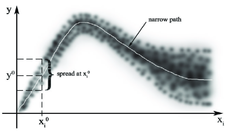
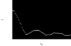
For any MISO system, IDS method considers N 2-dimensional discrete planes which N is the number of inputs in this MISO system and in the ith plane, vertical and horizontal axes are y and respectively. Then, each of the available input-output training data is spread on all of these planes such as the one shown in Fig. 1 which shows one of these planes after data spreading. This process is called “data spread” or “distilling ink drop” since it seems that at the coordinate specified by each of the input-output data, one ink drop has been distilled on each of these planes. As individual data spreads overlap each other, the overlapping regions become increasingly darker finally resulting in a pattern on each of the planes. By applying IDS method to constructed pattern image of each plane, two different types of information would be extracted. One is the narrow path and the other is the deviation of the spread data points around each narrow path (see Fig. 1). Narrow path in the ith plane shows the overall relationship between the output of the system, y, and the ith input while the spread of the data points around this path shows the importance degree of in system behavior. For example, if the spread of data points around narrow path be sufficiently small in the plane compared to other planes, it means that the importance degree of the input is higher than any other inputs. In other word, in this case MISO system can be approximately simplified to the SISO system described by the narrow path in the -y plane.
At the arrival of any new input vector , for determining the corresponding output by inference, values of narrow paths and spreads should be calculated at this point from the pattern images of the planes. These values are then transferred from IDS units to the upper layer for being used for the inferential process in the ALM. ALM uses these information and approximates output value. Here, we do not concern with how ALM performs inference, instead, we will only concentrate on hardware implementation of data spreading and extraction of narrow path and spread values.
Different schemes can be defined for extracting narrow path and spread from the pattern image in each of the planes. Hereafter, in order to have simple hardware implementation and not involving in exact mathematical techniques, narrow path and spread are computed as described below. Assume that a new input data is observed and we want to calculate values of narrow paths and spreads from the pattern images of planes at this input point. Without loss of generality, consider the pattern image after data spreading in plane (such as the one shown in Fig. 1). The number of cells in the column of this plane correspond to which have ink more than the predetermined value can be considered as a spread value at this point. Moreover, will be the value of narrow path at this point provided that the sum of the ink of the cells above be equal to the sum of the ink of the cells below it. This procedure can be repeated for each of the planes for extracting values of narrow paths and spreads at input point .
Using these definitions for narrow path and spread, in Section IV we present a new memristor crossbar-based structure as a hardware implementation of IDS method.
III Memristor
Publication of a paper [6] in Nature by Hewlett Packard labs in May 1, 2008, which announced the first experimental realization of the memristor whose existence was predicted in 1971 by Leon Chua [7] has caused an extraordinary increased interest in this passive circuit element. It has become clear that memristor can have many potential applications such as non-volatile memory construction [9], creation of analog neural network and emulation of human learning [11], building programmable analog circuits [12] and in signal processing field [13, 14, 15].
Memristor (), different from other electrical parameters namely resistance, capacitance and inductance, denotes the relationship between magnetic flux() and electric charge () as [7]:
| (1) |
By rewriting this equation, memristance can be expressed as:
| (2) |
which shows that the unit of memristance is ohm. A memristor can be thought of as a resistive device that its resistance varies in dependence of its current or magnetic flux.
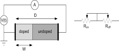
Memristor is an electrically switchable semiconductor thin film sandwiched between two metal contact with a total length of and consists of doped and un-doped regions which its physical structure with its equivalent circuit model is shown in Fig. 2 [6]. The internal state variable determines the length of doped region with low resistance against un-doped region with high resistivity. This internal state variable and consequently the total resistivity of the device can be changed by applying external voltage bias [8]. If the doped region extends to the full length , the total resistance of the device will be at its lowest level denoted as and If the un-doped region extends to the full length , the total resistance of the device will be at its highest level namely . Thus, the mathematical model for the total resistance of the memristor can be written as [6]:
| (3) |
where is the initial state for state variable , is the average ion mobility and is the amount of electric charge (integral of current) that has passed through the device. Above equations show that passing current from memristor in one direction will increase the resistance while changing the direction of the applied current will decrease its memristance. On the other hand, it is obvious that in this element, passing current in one direction for longer period of time (which means has higher absolute value) will change the resistance of the memristor more.
As a result, memristor is nothing else than the analog variable resistor which its resistance can be adjusted by changing the direction and duration of the applied voltage. Therefore, memristor can be used as a storage device in which analog values can be stored as an impedance instead of voltage.
IV Memristor crossbar-based hardware implementation of IDS method
IV-A Using memristor crossbar for data spreading
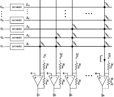
Figure 3 shows a memristor crossbar circuit that we have proposed as a hardware implementation of data diffusing process in IDS method. This memristor crossbar which is considered as one of the N discrete 2-dimensional planes for data spreading works as follows. This crossbar consists of two sets of horizontal and vertical wires which each wire in one of these sets is perpendicular to all of wires in the other set. The region where a wire in one set crosses over a wire in the other set is called a junction (or crosspoint). In this particular crossbar, memristor is formed in each junction between two passing wires. In this case, memristors in the crosspoints can be configured (their resistances can be changed) by applying suitable voltages to these two perpendicular wires. For example, memristance of the memristor located at the crossing point of the first horizontal and the first vertical wires of the crossbar correspond to coordinate (1, 1) (denoted by in Fig. 3) can be increased by applying a positive voltage to the first column of the memristor crossbar while grounding the first horizontal wire. Dropping positive voltage across the memristor will cause the current to flow through it which will increase the memristance of this passive element. On the other hand, reversing the polarity of the applied voltage will decrease the memristance of the memristor. Moreover, as (III) indicates, application of higher voltages for longer period of time will increase the memristance of the memristor more. This means that data can be stored in crosspoints through the memristances of the memristors.
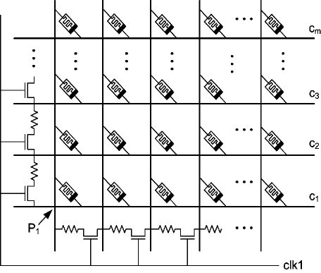
For utilizing this memristor crossbar structure for data spreading, each wire should be connected to its predecessor and successor wires by a simple resistor which can be done in Fig. 3 by setting clk1 input pin into logic 1. As it will become clear soon, resistance value of these resistors is inversely related to the effecting radius of ink drops. Higher resistances will yield to the lower effecting radius. Note that rows of the memristor crossbar shown in Fig. 3 are connected to the inputs of the circuit shown in Fig. 5.
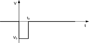
Suppose that initially all of the memristors in the crossbar have their highest possible memristance value, i.e. . Dropping ink at any arbitrary point (, ) can be accomplished by grounding the horizontal wire corresponding to and applying a finite duration negative pulse (such as the typical one shown in Fig. 4) to the vertical wire related to index . In this case, the current passing through the memristor at point (, ) will be maximum and hence, its resistance will be decreased more than any other memristors in the crossbar. Since all of rows or columns of the crossbar are connected to each others with resistors, by applying this negative pulse, current will pass through all of the memristors in the crossbar. However, by moving away from coordinate (, ) in each direction, the amount of current flowing through the memristors will be reduced (because of the resistors connected between columns or rows of the crossbar) and therefore their memristances will be decreased less than those which are nearer to the coordinate (, ). Note that in order to prevent unwanted feedback paths within the crossbar, a rectification layer may be provided or p-type and n-type doping may be performed creating diode junctions at each crosspoint. Next ink will be dropped in the same manner. Distilling of each ink drop will decrease the memristance of the memristors more (but with different amounts depending to their distances from the dropping point) and by this means, newly dropped ink will be added to the previously stored ink pattern.
Here, it is worth to mention that since dropping each ink drop alters memristance values of all of the memristors in the crossbar, changes caused in memristances by distilling two ink drops at the same coordinate (, ) but in different times will not be the same. This is because of the fact that passing current from memristors in these two cases are not the same. For relaxing this drawback, it is necessary that be much higher than the maximum amount of changes that can be made in the memristances of the memristors during ink dropping procedure. One of the particular advantages of this structure is that stored pattern image (as the memristances of memristors) will be fixed for theoretically infinite period of time without a need for being refreshed.
Note that for MISO system with N inputs, N memristor crossbars are needed as N 2-dimensional discrete planes in IDS method. After dropping all of the training input-output data onto these memristor crossbars, now they can be used in inferential process in IDS method.
IV-B Extraction of narrow path and spread values from pattern images stored in memristor crossbars
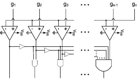
In ALM, with the incoming of any new input , inference is done only through the values of narrow path and spread functions at this point which have been computed by IDS method. As a result, totally computation and storing of narrow path and spread functions for every planes are not necessary. Instead, for any input data, computation of the values of these two functions for each of the input-output at this point planes will be sufficient for doing inference. Fig. 5 shows the circuit that we have proposed for doing these computations. The inputs of this circuit, i.e. for where m is the number of rows of the crossbar, are connected directly to the horizontal wires of the memristor crossbar. However, for having better understanding and because the overall circuit was too much large, we have split the whole circuit into two parts shown in Figs. 3 and 5. The crossbar in this figure (Fig. 5) is the same as the previously described memristor crossbar but by this difference that in those crosspoints which are specified by black dots, instead of memristor, resistive junctions with a resistance are being fabricated. In other crosspoints, there is no junction between two perpendicular wires. As can be seen in Fig. 5, each column of this resistive crossbar is connected to an opamp having resistor with resistance value as a feedback (except the last one which its feedback resistor is ). Note that the combination of resistors of the resistive crossbar and these opamps creates a opamp-based summing circuits. In this case, outputs of these opamps denoted by for can be written as:
| (4) |
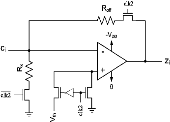
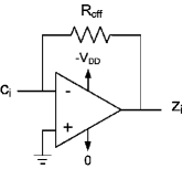
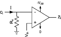
where is a constant positive value which will be defined in the next paragraph and n=m is the number of columns in resistive crossbar. Internal circuit of the connector blocks used in Fig. 5 and connecting memristor and resistive crossbars is depicted in Fig. 6. To compute narrow path, these blocks are configured as a simple current to voltage convertor (such as the one shown in Fig. 6) by setting clk2 input pin in Fig. 6 into logic 1. On the other hand, for the calculation of the spread value, connector blocks are configured as a circuit shown in Fig. 6 by setting clk2 input pin into logic 0. This circuit converts the input current I into voltage through the resistor and then compares it with the pre-specified value . Therefore, this circuit can be used for thresholding.
Now, let’s see how our proposed circuit can calculate narrow path and spread functions from the pattern image stored in memristor crossbar. For computing narrow path in this plane (memristor crossbar) at any specific point , the jth column of the memristor crossbar which corresponds to should be connected to the small positive voltage while other columns and rows are connected into high impedance. Note that in this case, clk1 input pin of the memristor crossbar should be set into logic zero. Smallness of the applied voltage is necessary for not changing the memristances of the memristors while computing a narrow path. Consequently, the output of the ith connector block configured as a current-to-voltage converter will be:
| (5) |
where is the memristance of the memristor at the crossing point of the ith row and jth column of the memristor crossbar after the ink dropping procedure. Equation (5) can be rewritten as:
| (6) |
where is the amount of change made to the memristance of the memristor located at coordinate (i, j) during the ink dropping process. As explained in previous section, since we have assumed that is much higher than (i.e. ), (7) can be simplified as:
| (7) |
| (8) |
Tarkhan et al. in [5] have proved that if be the index of the narrow path cell in the jth column of the crossbar, it will has the following interesting property:
| (9) |
By multiplying sides of this inequality by , we will get:
| (10) |
which is equal to the following inequality:
| (11) |
Therefore, the index of the narrow path cell can be simply found for instance by using the circuit depicted in Fig. 7. In this circuit, each opamp compares the input voltage with . Afterward, the combinational logic circuit specifies the first place that the input signal becomes higher than . Therefore, during the narrow path calculation phase, only one of the outputs of this combinational logic circuit will be at logic 1 which indeed indicates the location of narrow path cell.
Finding the value of the spread function at can be done from the same circuit shown in Fig. 5. If the jth column of the memristor crossbar which corresponds to is connected to the small negative voltage like (while other wires are connected to high impedance), then the voltage at the positive input terminal of the opamp in the ith connector block (which is configured as the circuit shown in Fig. 6) will be:
| (12) |
By setting (the voltage at the negative input terminal of the opamp in the ith connector block) to where is a predetermined constant value, output voltage of the ith connector block, , can be written as (see Fig. 6):
| (13) |
As we have stated at the beginning of this section, memristance of all of the memristors change during the ink dropping procedure. To calculate the spread function at , it is necessary to determine how many memristors on the jth column of the memristor crossbar are being affected considerably enough during the ink dropping process (see how the value of spread is determined in Fig. 1 at input point ). In (13), acts as a threshold. If (which represent the amount of ink dropped to the coordinate (i, j)) be higher than , the output of the ith connector block will be . Otherwise, the output will be zero. Since suitable value of does not require to be precise and in addition, it depends on so many factors such as , and the number of training data, it can be simply estimated for example by trial and error. Therefore, the value of the spread at can be approximated by the number of opamps (hereafter denoted by M) which their outputs are . This quantity can be computed through the current passing from the last vertical wire of the resistive crossbar, , which is shown in Fig. 5 and can be written as:
| (14) |
Consequently, this current is directly proportional to M and therefore can be considered as a value of the spread function at the presented input data. Hence, this proposed circuit, at any input data, can calculate the values of narrow path and spread functions in only two clock periods.
V Simulation results
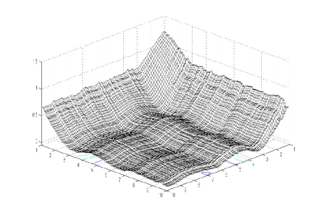
For investigating the accuracy of the proposed method, we conducted a modeling simulation. In this modeling test, the following nonlinear function is used:
| (15) |
where its graph is shown in Fig. 8. 800 randomly chosen data sets are used for this modeling test and each planes of IDS (such as the typical one shown in Fig. 3) has the resolution of 100x90. This means that each of these crossbars has 9000 memristors. Resistance of the resistors which are connecting rows or columns to each other in these memristor crossbars was set to 1000. These planes are simulated in HSPICE software by utilizing the SPICE model proposed in [16] for memristors.
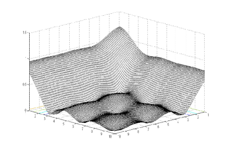
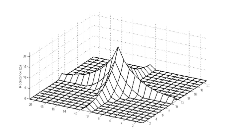
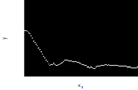
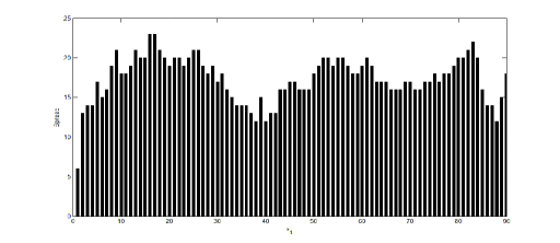
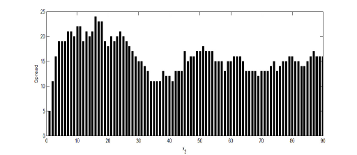
As explained in Section IV-A, distilling an ink drop at any point changes the memristance of the neighboring memristors in the crossbar. Figure 9 shows the absolute value of the amount of changes made to the memristance of the memristors near to the distillation point of one ink drop. Note that this result is obtained by setting , and into 100k, -3 volt and 10 milliseconds respectively. Results of spreading all of 800 training data sets on and planes are shown in Fig. 10 (note that these figures show for any of the memristors in the crossbar) and their corresponding computed narrow paths are depicted in Fig. 11. For the calculation of the spread at any input point from the planes shown in Fig. 10, we set into 20. Results computed by our proposed hardware for the values of spread () at any column of the planes shown in Fig. 10 are presented in Fig. 12. Finally, by passing these computed values for narrow path and spread functions to ALM, obtained modeling result for (15) is shown in Fig. 13.


VI Conclusion
In this paper a new hardware implementation of IDS method is presented based on the memristor crossbar structure. Proposed structure can compute narrow path and spread at any given input data in real-time since it is implemented in analog instead of digital. Furthermore, since input-output training data are stored in memristors at the crosspoints of the crossbar, system can continue working properly after the occurrence of power breakdown. However, since memristor can be realized in nanoscales, we confront some difficulties and technological challenges in the integration of nanoscale memristor crossbars and conventional electronics systems.
References
- [1] S.B. Shouraki, “A Novel Fuzzy Approach to Modeling and Control and its Hardware Implementation Based on Brain Functionality and Specifications,” Ph.D. dissertation, The Univ. of Electro-Communications, Chofu, Japan, March 2000.
- [2] S.B. Shouraki and N. Honda, “Recursive Fuzzy Modeling Based on Fuzzy Interpolation,” Journal of Advanced Computational Intelligence, Vol. 3, No. 2, pp. 114 125, April 1999.
- [3] M. Murakami and N. Honda, “A study on the modeling ability of the IDS method: A soft computing technique using pattern-based information processing,” International Journal of Approximate Reasoning, vol. 45, pp. 470–487, 2007.
- [4] M. Murakami, N. Honda and J. Nishino, “A High Performance IDS Processing Unit for a New Fuzzy-based Modeling,” IEEE International Conference on Fuzzy Systems, vol. 2, pp. 935–940, 2004.
- [5] M. Tarkhan, S.B. Shouraki and H. Khasteh, “A novel hardware implementation of IDS method,” IEICE Electron. Express, Vol. 6, No. 23, pp. 1626–1630, 2009.
- [6] D.B. Strukov, G.S. Snider, D.R. Stewart and R.S. Williams, “The missing memristor found,” Nature, 2008, vol. 453, pp. 80–83, 1 May 2008.
- [7] L.O. Chua, “Memristor - the missing circuit element,” IEEE Trans. on Circuit Theory, vol. CT-18, no. 5, pp. 507–519, 1971.
- [8] J.J. Yang, M.D. Pickett, X. Li, D.A. Ohlberg, D.R. Steward, and R.S. Williams, “Memristive switching mechanism for metal/oxide/metal nanodevices,” Nature Nanotechnology 3, pp. 429-433, 2008.
- [9] R. Waser, and M. Aono, “Nanoionics-based resitive switching memories,” Nature Materials 6, vol. pp. 833–840, 2007.
- [10] P. Kuekes, “Material Implication: digital logic with memristors,” Memristor and Memristive Systems Syymposium, 21 November 2008.
- [11] Y.V. Pershin, S.L. Fontaine, and M.D. Ventra, “Memristive model of amoeba’s learning,” arXive: 0810.4179v2, 24 October 2008.
- [12] S. Shin, K. Kim, and S.M. Kang, “Memristor-based fine resolution resistance and its applications,” ICCCAS 2009, July 2009.
- [13] B.L. Mouttet, “Proposal for Memristors in Signal Processing,” Nano-Net 2008, pp. 11–13, 2009.
- [14] B.L. Mouttet, “Crossbar comparator,” US Patent 7,564,262, 2009.
- [15] B.L. Mouttet, “Crossbar waveform driver circuit,” US Patent 7,576,565, 2009.
- [16] D. Biolek, Z. Biolek and V. Biolkova, “SPICE Modeling of Memristive, Memcapacitative and Meminductive Systems,” European Conference on Circuit Theory and Design (ECCTD2009), pp. 249–252, Antalya, 23–27 Augost 2009.