Gate-tunable split Kondo Effect in a Carbon Nanotube Quantum Dot
Abstract
We show a detailed investigation of the split Kondo effect in a Carbon nanotube quantum dot with multiple gate electrodes. Two conductance peaks, observed at finite bias in nonlinear transport measurements are found to approach each other for increasing magnetic field, to result in a recovered zero-bias Kondo resonance at finite magnetic field. Surprisingly, in the same charge state, but under different gate-configurations, the splitting does not disappear for any value of the magnetic field, but we observe an avoided crossing. We think that our observations can be understood in terms of a two-impurity Kondo effect with two spins coupled antiferromagnetically. The exchange coupling between the two spins can be influenced by a local gate, and the non-recovery of the Kondo resonance for certain gate configurations is explained by the existence of a small antisymmetric contribution to the exchange interaction between the two spins.
pacs:
72.15.Qm,73.63.Kv,73.21.La,73.23.Hk,73.63.FgThe Kondo effect, the screening of a localized magnetic impurity by a surrounding Fermi gas, is one of the most prominent examples of correlated electron systems Hewson93 . The observation of the Kondo effect in quantum dots has sparked renewed interest in the exploration of this correlation effect, as quantum dots are highly tunable, and a lot of different parameter regimes of a Kondo state can be realized Goldhaber98 ; Cronenwett98 . Single-wall Carbon nanotubes can be used for the production of quantum dot devices, and allow for the study of the Kondo effect, as they usually show a strong confinement potential, a fact that leads to a large Kondo energy scale Nygard00 . Carbon nanotubes can moreover be contacted by superconducting Morpurgo99 and ferromagnetic Tsukagoshi99 ; Sahoo05 electrodes, and therefore allow the production of hybrid devices incorporating non-normal metal contacts. One aspect in which Carbon nanotube quantum dots are less versatile than e. g. lateral quantum dots, that are also widely used to study the Kondo effect, is the control over the contact transparencies and their asymmetry, two key parameters for the Kondo effect. The total transparency is usually given after production of a CNT quantum dot, and can only be changed in a small range by driving the backgate over a large voltage. The contact asymmetry can vary slightly between different charge states Eichler09 , but up to now cannot be controlled systematically.
Here, we report on an experiment performed on a Carbon nanotube quantum dot with two additional, local gate electrodes. The local gates, fabricated as topgates on a thin, high- oxide layer were placed above the interface between the metal contact and the Carbon nanotube, in an attempt to localize their gating effect to the area close to the metal-nanotube interface. The coupling of the quantum dot to the leads is in the intermediate regime, where Coulomb interactions and Kondo correlations dominate the electronic transport. We observe a split Kondo resonance, with a zero field splitting of 120 eV. As we will point out below, this observation is consistent with a two-impurity Kondo effect, with two electrons coupled to each other antiferromagnetically. In this sense, our experimental situation is similar to previous experiments on lateral quantum dots Craig04 , although in our case, the two-spin configuration is more accidental.
A device schematic together with a scanning electron micrograph of a device equivalent to the one that was measured is presented in figure 1. Single-wall Carbon nanotubes are grown on thermally oxidized silicon wafers by the chemical vapor deposition method. We select individual, straight nanotubes with a scanning electron microscope and define source (S) and drain (D) electrodes by e-beam lithography. A thin (5 nm) layer of Al2O3 is then grown over the whole device by atomic layer deposition (ALD) in a Cambridge Nanotech Savannah ALD system. In a last lithography step palladium topgates are defined. A backgate voltage is applied to the highly doped silicon substrate. The sample is glued into a nonmagnetic chip carrier and wire-bonded. We cool the sample in a dilution refrigerator to a temperature of mK and measure the differential conductance through the device with a lock-in technique under a constant AC voltage bias of V. The aluminum contacts are superconducting below K, but we will in the following concentrate on electrical transport under a magnetic field , that is applied in the plane of the wafer, under an angle of about to the nanotube axis as indicated in figure 1b. The effect we discuss emerges for T, when superconductivity is suppressed and the leads behave as normal metals. is measured as a function of magnetic field , voltage , backgate and the voltage on one topgate , with the second topgate floating. The backgate is expected to affect the whole device, whereas the topgate should gate more locally, in the vicinity of the CNT-metal contact interface. Large range gate voltage sweeps revealed, that the nanotube in the device presented here was metallic.
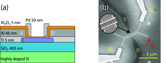
Figure 2a shows a measurement of as a function of and at zero bias voltage () and for T. We can clearly distinguish resonances in , corresponding to positions where an electronic level on the quantum dot is energetically aligned with the chemical potential of the contacts. The values of for which this occurs shift with . The slope of the resulting lines in the colorscale plot of in figure 2a is not constant, however, but we observe regions where two resonances approach and the differential conductance between them increases (dashed frames). We shall see that this can be attributed to a Kondo resonance whose energy and characteristics can be tuned by . Charge rearrangements leading to jumps in the electrostatic potential of the quantum dot can be seen as discontinuities in the colorscale plot of in figure 2a. As these jumps occur more frequently in the present device compared to devices without topgates, we assume that they are due to trapped charge in the topgate oxide. The jumps do not occur frequent enough however, to prohibit a careful study of the device.
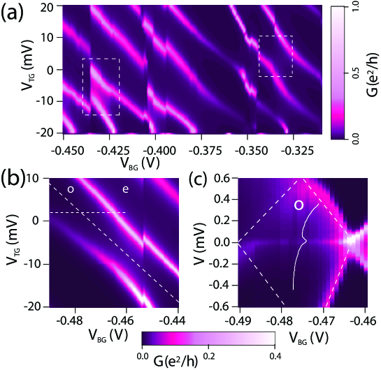
For a detailed analysis, we concentrate on the ranges of and plotted in figure 2b. We denote two charge states by o (odd) and e (even) in anticipation of a spin- Kondo effect in o. The horizontal dashed line marks the position of the measurement of versus and displayed in figure 2c. From the size of the Coulomb diamond in this plot, we extract a charging energy of about meV (white dashed lines). In addition, a ridge of high differential conductance shows up around zero bias, which we identify as signature of the spin- Kondo effect.
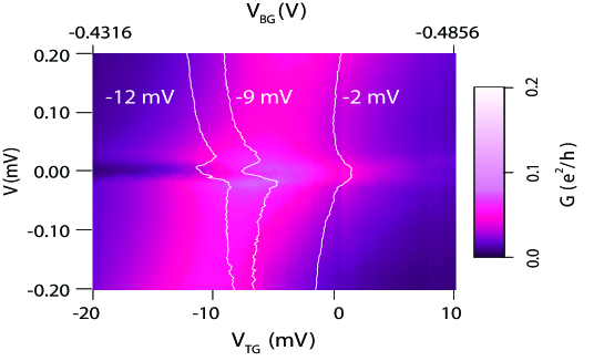
Changing both and in the right way, we can modify the electrostatic confinement potential of the dot while keeping the chemical potential and the occupation constant. In figure 3 we show a measurement of the nonlinear conductance for a range of gate voltages that are indicated by the slanted dashed line in figure 2b and that correspond to the middle of the charge state denoted as o. We can follow the development of the Kondo feature from a zero bias peak ( mV) into two peaks at finite voltage ( mV). The width of the peak at mV is of the order of V, corresponding to a Kondo temperature of about K.
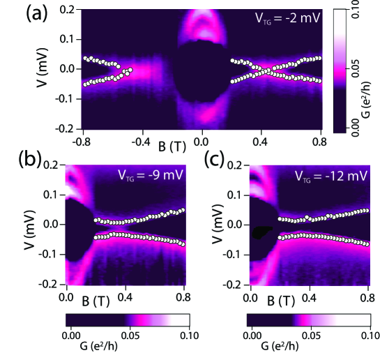
To gain more insight into the origin of the splitting observed in figure 3, we have measured the nonlinear conductance as a function of magnetic field for three fixed gate configurations, corresponding to three different points on the dashed line in figure 2b. In figure 4a, we present data for ( mV, V). At low field, superconductivity dominates electrical transport, preventing the appearance of the Kondo effect. For T, superconductivity is suppressed, and we can follow the evolution of the two spin components of the Kondo ridge in the external magnetic field. From the slope of these lines, we estimate , a value that is consistent with a free electron g-factor plus some small orbital magnetic moment contribution that could be present Minot04 , as the magnetic field was applied under an angle of to the axis of the nanotube. The Kondo resonance is recovered only at a finite magnetic field of T. Note that except for a very small shift of T, that is probably due to flux trapping in the superconducting magnet, the data for positive and negative magnetic field are equivalent. Extrapolating the high conductance lines towards , we find a zero field splitting of .
A qualitatively different picture evolves at two other positions in the -plane of figure 2b : For (-9 mV/-0.456 V) (figure 4b) and (-12 mV/-0.453 V) (figure 4c), the Kondo resonance is not recovered for any value of magnetic field, but instead the two high conductance lines only approach each other up to a minimum distance of about V, giving an anti-crossing like behavior. Note that both of these points correspond to the middle of the same charge state as the measurement in figure 4a. Extrapolating to gives roughly the same zero field splitting eV, and the slope of the two high conductance lines, taken at higher magnetic fields, is the same as for the data in figure 4a.
At first sight our data bear a striking resemblance to data obtained on a Carbon nanotube quantum dot with ferromagnetic contacts Hauptmann08 . In this experiment, a splitting of the Kondo resonance at as well as its recovery at finite magnetic field could be explained with the presence of an exchange field, that is induced by the magnetization of the ferromagnetic electrodes Martinek03 ; Martinek05 . An avoided crossing similar to the one in figures 4b/c had been observed in some samples in Hauptmann08 , and was explained with a small misalignment of the exchange field with respect to the external magnetic field, a situation which would expose the impurity spin to a finite magnetic field for all values of the external magnetic field, and therefore prevent the recovery of the Kondo resonance. This misalignment is however given by the domain structure of the ferromagnetic electrodes, and cannot be changed by gate voltages. Moreover, the existing theories for a ferromagnetic exchange field acting on a single spin in a quantum dot Martinek03 ; Martinek05 predict the induced exchangefield to always be parallel (or anti-parallel) to the magnetization of the electrodes, a misalignment of the two is not possible. Additionally, we have not deliberately introduced any ferromagnetic parts into our sample, and therefore have to discard an explanation in terms of a ferromagnetic exchange field.
There have been reports of a split Kondo effect in CNT quantum dots Nygard04 , where the coupling to a ferromagnetic catalyst particle, that is needed to synthesize the Carbon nanotube Kong98 , has been discussed as the origin of a ferromagnetic exchange field that could split the Kondo resonance at . However, as the catalyst particles normally stick to the end of the nanotube (at several m distance from the quantum dot), and are extremely small (1-2 nm, equivalent to the nanotube diameter), we do not think that they can account for an exchange field on the dot of the order of T. We believe that the nonlinear temperature dependence of the equilibrium conductance at reported in Nygard04 rather points to a two-impurity Kondo effect as the origin of the observed splitting of the Kondo resonance.
The Kondo effect in the presence of two magnetic impurities has been investigated first theoretically Jayaprakash81 ; Tolea07 ; Chang09 and later experimentally vanderWiel02 ; Craig04 . In quantum dots, a two-impurity Kondo effect can occur in a parallel double quantum dot or in a single dot with two near-degenerate levels. Two electrons (impurities) that can interact with each other via exchange interaction, and that interact independently with the Fermi sea in the leads, are considered. Depending on temperature, magnetic field, strength and sign of the inter-impurity exchange interaction, the occurrence of the Kondo effect is qualitatively different from the simple spin- Kondo effect. Here we will consider a situation where one of the impurities is fixed, and doesn’t participate in transport, e. g. an electron localized in a trap state in the gate oxide close to the nanotube. However, it will still interact with the spin of the second impurity via some exchange interaction
| (1) |
Such a situation has been realized in a serial triple quantum dot device Craig04 , where the two outer dots held the impurity spins, and the larger middle dot functioned as a small Fermi reservoir, mediating a tunable Ruderman-Kittel-Kasuya-Yoshida (RKKY) like exchange interaction. This experiment has been described theoretically in Refs. Simon05 ; Vavilov05 . Common to both ferromagnetic and antiferromagnetic exchange interaction between the two impurities is a suppression of conductance at for zero magnetic field, which results in a split Kondo resonance. To distinguish between ferro- and antiferromagnetic exchange between the two electrons, one has to look at the magnetic field dependence Simon05 ; Pustilnik01 ; Chung07 ; Aono01 , as only for antiferromagnetic exchange () the two peaks approach each other with increasing magnetic field, and the Kondo resonance can be recovered at finite B. In case of ferromagnetic exchange (), the magnetic field dependence of the two maxima in is much weaker, and a more complicated two stage Kondo effect will occur at low enough temperature. In the case of , the antiferromagnetic interaction between the two unpaired spins is competing with the Kondo screening, the two impurities are locked into a singlet, and the Kondo effect is inactive, which leads to a suppression of conductance at . Only for larger energies, when transition from the singlet into the lowest triplet state can take place, the Kondo screening will be reestablished and two maxima in at will occur Simon05 . As the two maxima in this case correspond to a singlet/triplet degeneracy point, they will change their position with magnetic field and allow for a recovery of the Kondo resonance at the magnetic field induced crossing between the singlet and lowest triplet state.
With this scenario in mind, we can explain the data shown in figure 4a. The observed zero-field splitting of eV would correspond to the exchange constant between the electron spin and an additional spin, that is fixed, either in a second dot somewhere on the nanotube, or at a defect in the gate oxide close to the nanotube. An exchange constant of the order of eV is realistic Craig04 . The approaching of the two maxima and the recovery of the Kondo resonance at T also correspond to the theoretical prediction, and are qualitatively similar to experimental results reported previously Heersche06 ; Osorio07 ; Otte09 . The effects of a fixed impurity spin have also been investigated in two recent experiments on Carbon nanotube quantum dots Bomze10 ; Chorley10 .
To explain the data of figures 4b/c in this scenario, we have to extend the inter-impurity exchange interaction by an antisymmetric, Dzyaloshinskii-Moriya (DM) type component
| (2) |
Dzyaloshinskii58 ; Moriya60 , which would prevent the complete anti-parallel alignment of the two spins, having the same effect as a misaligned exchange field in a dot with ferromagnetic contacts Hauptmann08 . As the presence of a second, fixed spin, and the exchange interaction of this fixed spin with the dot spin in our sample is not well controlled and rather accidental, such a situation is imaginable. Similar to the exchange constant , the vector is a property of the two-spin system and in the case of the DM interaction is determined by spin-orbit interaction. It is therefore possible that the direction and length of are sensitive to the electrostatic environment of the two spins, so that can be gate dependent. To our knowledge, there are no previous reports of antisymmetric exchange interactions in quantum dots, although there is some theoretical work on electronic transport through a molecular magnet that is composed of two spins with DM interaction Herzog10 . This work however examines the level spectrum of the molecular magnet as observed from excited state lines in sequential tunneling through a weakly coupled quantum dot. A two-impurity Kondo effect with spin-orbit coupled conduction electrons has been investigated in Mross09 , and the Kondo effect in a quantum dot with an even number of electrons in the presence of spin-orbit interaction has been investigated in Lucignano10 . However, we are however not aware of any theoretical work that corresponds to our experimental situation with an odd number of electrons on the dot and on-site spin-orbit interaction.
To support the explanation in terms of a two-impurity Kondo effect, a detailed determination of the temperature dependent conductance would be desirable. Unfortunately, due to the bad electrostatic stability on longer timescales, this has not been possible for the present device. We note, however, that the non-monotonic temperature dependence observed in Nygard04 corresponds to the prediction for a two-impurity Kondo effect, as given e. g. in Simon05 .
In conclusion, we have shown a split Kondo effect in a Carbon nanotube quantum dot with additional, locally acting gates. The zero-bias Kondo resonance can be recovered at a finite magnetic field, a situation consistent with a two-impurity Kondo effect of two spin 1/2 particles that are linked by an antiferromagnetic exchange interaction. A slight deformation of the dot confinement potential by one of the local gates led to a situation where the Kondo resonance could no longer be recovered, but where the two high conductance lines form an anti-crossing, with a minimum distance of about eV. We speculate that this anti-crossing might be due to the occurrence of a small antisymmetric component in the exchange interaction between the two Kondo impurities, which becomes active for certain gate voltages and prevents a complete compensation of the impurity spin by the Fermi sea in the leads. Further experimental and theoretical work will be needed to unambiguously support this picture.
Acknowledgements
Financial support from the EU-FP6 project HYSWITCH, the Swiss National Science Foundation, and the NCCR on Nanoscale Science is acknowledged. M. W. is a grantee of the Treubel Fund. We thank Pascal Simon and Mahn-Soo Choi for fruitful discussion.
References
References
- (1) A. C. Hewson, The Kondo Problem to Heavy Fermions, Cambridge University Press, (1993)
- (2) D. Goldhaber-Gordon, H. Shtrikman, D. Mahalu, D. Abusch-Magder, U. Meirav, and M. A. Kastner, Nature 391, 156 (1998)
- (3) S. M. Cronenwett, T. H. Oosterkamp, and L. P. Kouwenhoven, Science 281, 540 (1998)
- (4) J. Nygard, D. H. Cobden, and P. E. Lindelof, Nature 408, 342 (2000)
- (5) A. F. Morpurgo, J. Kong, C. M. Marcus, and H. Dai, Science 286, 263 (1999)
- (6) K. Tsukagoshi, B. W. Alphenaar, and H. Ago, Nature 401, 572 (1999)
- (7) S. Sahoo, T. Kontos, J. Furer, C. Hoffmann, M. Gräber, A. Cottet, and C. Schönenberger, Nature Physics 1, 99 (2005)
- (8) A. Eichler, R. Deblock, M. Weiss, C. Karrasch, V. Meden, C. Schönenberger, and H. Bouchiat, Phys. Rev. B 79, 161407(R) (2009)
- (9) N. J. Craig, J. M. Taylor, E. A. Lester, C. M. Marcus, M. P. Hanson, and A. C. Gossard, Science 304, 565 (2004)
- (10) E. D. Minot, Y. Yaish, V. Sazonova, and P. L. McEuen, Nature 428, 536 (2004)
- (11) J. R. Hauptmann, J. Paaske, and P. E. Lindelof, Nature Physics 4, 373 (2008)
- (12) J. Martinek, Y. Utsumi, H. Imamura, J. Barnas, S. Maekawa, J. König, and G. Schön, Phys. Rev. Lett. 91, 127203 (2003)
- (13) J. Martinek, M. Sindel, L. Borda, J. Barnas, R. Bulla, J. König, G. Schön, S. Maekawa, and J. von Delft, Phys. Rev. B 72, 121302R (2005)
- (14) J. Nygård, W. F. Koehl, N. Mason, L. DiCarlo, and C. M. Marcus, unpublished (arXiv:cond-mat/0410467v2)
- (15) J. Kong, H. T. Soh, A. M. Cassell, C. F. Quate, and H. Dai, Nature 395, 878 (1998)
- (16) C. Jayaprakash, H. R. Krishna-murty, and J. W. Wilkins, Phys. Rev. Lett. 47, 737 (1981)
- (17) M. Tolea, and B. R. Bulka, Phys. Rev. B 75, 125301 (2007)
- (18) A. M. Chang, and J. C. Chen, Rep. Prog. Phys. 72, 096501 (2009)
- (19) W. G. van der Wiel, S. De Franceschi, J. M. Elzerman, S. Tarucha, L. P. Kouwenhoven, J. Motohisa, F. Nakajima, and T. Fukui, Phys. Rev. Lett. 88, 126803 (2002)
- (20) P. Simon, R. Lopez, and Y. Oreg, Phys. Rev. Lett. 94, 086602 (2005)
- (21) M. G. Vavilov, and L. I. Glazman, Phys. Rev. Lett. 94, 086805 (2005)
- (22) M. Pustilnik, and L. I. Glazman, Phys. Rev. B 64, 045328 (2001)
- (23) C.-H. Chung, and W. Hofstetter, Phys. Rev. B 76, 045329 (2007)
- (24) T. Aono, and M. Eto, Phys. Rev. B 64, 073307 (2001)
- (25) H. B. Heersche, Z. de Groot, J. A. Folk, L. P. Kouwenhoven, H. S. J. van der Zant, A. A. Houck, J. Labaziewicz, and I. L. Chuang, Phys. Rev. Lett. 96, 017205 (2006)
- (26) E. A. Osorio, K. O’Neill, M. Wegewijs, N. Stuhr-Hansen, J. Paaske, T. Bjornholm, and H. S. J. van der Zant, NanoLetters 7, 3336 (2007)
- (27) A. F. Otte, M. Ternes, S. Loth, C. P. Lutz, C. F. Hirjibehedin, and H. J. Heinrich, Phys. Rev. Lett. 103, 107203 (2009)
- (28) Y. Bomze, I. Borzenets, H. Mebrahtu, A. Makarovski, H. U. Baranger, and G. Finkelstein, Phys. Rev. B 82, 161411R (2010)
- (29) S. J. Chorley, G. Giavaras, J. Wabnig, G. A. C. Jones, C. G. Smith, G. A. D. Briggs, and M. R. Buitelaar, unpublished (arXiv:1004.4377v1)
- (30) I. Dzyaloshinskii, J. Phys. Chem. Solids 4, 241 (1958)
- (31) T. Moriya, Phys. Rev. 120, 91 (1960)
- (32) S. Herzog, and M. R. Wegewijs, Nanotechnology 21, 274010 (2010)
- (33) D. M. Mross, and H. Johannesson, Phys. Rev. B 80, 155302 (2009)
- (34) P. Lucignano, M. fabrizio, and A. Tagliacozzo, Phys. Rev. B 82, 161303R (2010)