Valley-dependent Brewster angles and Goos-Hänchen effect in strained graphene
Abstract
We demonstrate theoretically how local strains in graphene can be tailored to generate a valley polarized current. By suitable engineering of local strain profiles, we find that electrons in opposite valleys ( or ) show different Brewster-like angles and Goos-Hänchen shifts, exhibiting a close analogy with light propagating behavior. In a strain-induced waveguide, electrons in and valleys have different group velocities, which can be used to construct a valley filter in graphene without the need for any external fields.
pacs:
73.22.-f 73.23.-b 73.40.Gk 85.30.DeIntroduction. In recent years, graphene, a single layer of carbon atoms arranged in a hexagonal lattice has shown abundant new physics and potential applications in carbon-based nanoelectronic devices. Novoselov2 ; Zhang ; Neto The novel properties arise from the linear energy dispersion and the chiral nature of electrons at the and valleys of the Brillouin zone. Neto Mathematically, the Dirac equation describing the motion of massless quasiparticles is very similar to the Helmholtz equation for an electromagnetic wave, except for the negative energy spectrum. This remarkable fact could make it possible to observe optical-like electron propagating behavior and to construct Dirac electron-optical devices with graphene. Cheianov The mean-free path of electrons in graphene can approach microns at room temperature, making electrons behave ballistically in a graphene microstructure. Ozyilmaz ; Morozov In such a ballistic regime, the scattering of electrons by potential barriers can be understood by comparing with the reflection, refraction and transmission of electromagnetic waves in inhomogeneous media. Therefore, graphene is a testbed to examine optical-like phenomena of Dirac fermions. Several studies have been devoted to such optical-like electron behaviors using external electric bias. Cheianov ; Park ; Darancet ; Goos ; Chen ; Beenakker ; Ghosh ; Zhao ; Concha ; Williams These proposals require to deposit a metallic gate above graphene, which is an additional complication.
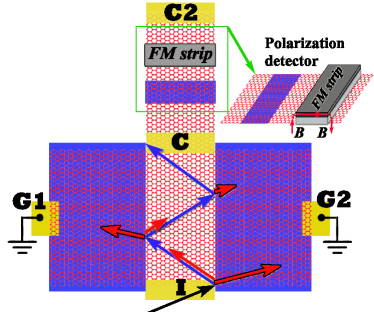
The strain effect in graphene provides a new way to manipulate electron transport without external fields. The two valleys in graphene are related by time reversal symmetry and act in much the same way as electron spin in spintronics. The valley degree of freedom in graphene might be used to control the characteristics of graphene-based devices, referred to as valleytronics. Xiao ; Pereira ; Rycerz Realization of such valleytronics requires an effective and robust scheme to produce valley polarized currents, although several schemes about valley filters were proposed utilizing, e.g., the edge profile of graphene nanoribbons, the trigonal warping effect in the energy spectrum, and intense irradiation on a bilayer graphene. Rycerz ; ZZZhang ; JMPJ ; Abergel In this letter, we propose a simple and effective way to realize some optical-like behaviors of electrons and valley filters by using the strain effect alone. We find that electrons in opposite valleys can be perfectly transmitted or totally reflected in the presence of strain. A quantum waveguide formed between two strained regions (see Fig. 1) can confine electrons in it and the reflected beam is shifted laterally along the interface by a distance with respect to the incident beam, as the Goos-Hänchen (GH) effect Goos in optics. We demonstrate that the valley-dependent GH effect in graphene results in different group velocities for electrons in and valleys.
Model. Mechanical strain in graphene can be described by a gauge vector potential. To illustrate the operating principle of the proposed device, we take a simplified gauge field which is equivalent to a delta-function-like antiparallel magnetic double barrier perpendicular to the graphene monolayer, but with opposite direction at and valleys. Bao ; Guinea The Landau gauge is adopted in our calculation. The length scale of the spatial variation of the pseudo gauge vector potential is much larger than the lattice spacing of graphene, which implies that intervalley scattering is weak at low-energy regions. The low-energy electrons can be well described by the effective Hamiltonian , Pereira where the superscript indicates the different regions (see Fig. 2), is the Fermi velocity, are the pseudospin Pauli matrices, is the electron momentum, is the electrostatic potential in the region , and labels and valleys. In the calculation, we introduce the dimensionless length and energy units: , (which are nm and meV for a typical pseudomagnetic field T).
Brewster-like Angle. We start by investigating electron transmission through a region of uniform uniaxial strain with width as shown in the inset of Fig. 2. Here, we set for simplicity since the key physical mechanism to introduce the valley-dependent Brewster angle is the gauge vector . The translational invariance along the y direction gives rise to conservation of transverse wave vector , and thus the solutions can be written as . In the strained region, the longitudinal wave vector has a different dependence on the vector potential for the two valleys denoted by , since the strain-induced pseudomagnetic fields have different signs for the two valleys. The reflected amplitude reads
| (1) |
where the incident and refractive angles are defined as and . These expressions are valid for incident angle . is the critical angle for total reflection in optics and gives Snell’s law for transmitted electrons. Note that when , the refractive index of the strained graphene is negative just like for a metamaterial with a negative refractive index. Importantly, one can tune the refractive index mechanically in quite a large range, which is not so for the metamaterials. When , electron beams can be totally reflected at such a strained barrier, since the longitudinal wave vector becomes imaginary accounting for the occurrence of evanescent modes in the barrier.
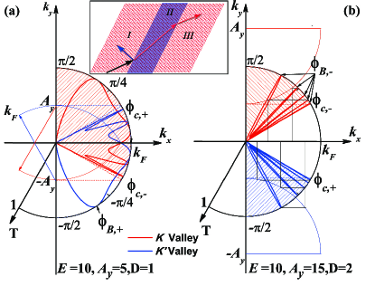
Figure 2 shows the angular dependence of the transmission probability , which exhibits a remarkable valley-dependence. It is obvious that , where , i.e., the transmission of electrons in and valleys shows a mirror symmetry about . This feature is guaranteed by the time reversal symmetry in strained graphene. In the presence of uniform uniaxial strains, the wave vectors of electrons in valley satisfy the relationship as indicated by the red arc curve. When , (equivalent to ), the wave vector in the strained region becomes imaginary, indicating the appearance of evanescent modes, thus transmission is totally blocked. The critical angle for total reflection is given by Snell’s law, . Thus the transmission window of electrons in valley is restricted to the red shadowed region (), as shown in Fig. 2(a). In contrast, the transmission of electrons in valley shows mirror symmetry behavior with respect to that in valley. Similarly, the critical angle for electrons in valley is given by . As a consequence, there exist mirror symmetric transmission windows for and electrons that can be completely separated by increasing the strain gauge fields [Fig. 2(b)]. One can see in Fig. 2 that for some specific incident angles , resonant peaks that reach perfect transmission exist in different windows for electrons in or valley. This can be readily checked by analyzing the zeros of the reflected amplitude corresponding to . The perfect tunneling peaks are fully coincident for [see Fig. 2(b)]. The number of resonant peaks increases with the incident energy and the width of the strained region. Note that if such resonant peaks for one valley are located in the transmission gap for the other valley , we can obtain valley- polarized transmitted electron beams and valley- polarized reflected beams. These characteristic angles are analogous to the so-called Brewster angle in optics, at which s- and p-polarized light are produced. We can propose a valley polarization device that is straightforward and analogous to the Glan-Thompson optical polarizers. The strained stripe leads to perfect transmission of one valley component and total reflection of the other valley components when electron beams are incident at the Brewster-like angles .
Valley-dependent Goos-Hänchen Effect. In analogy with total reflection of light at the interface between two materials with different refractive indexes, the electronic GH effect describes the shift of the reflected electron beam for total internal reflection at an interface, along the transverse direction. The GH shift could be positive or negative which is determined by external electric Beenakker and/or inhomogeneous magnetic fields Chen , an analogue with the optical GH effect in normal materials or metamaterials. A uniform uniaxial strain in graphene can lead to a valley-dependent GH shift , where is the modulus of the imaginary wave vector in the strained region in the case of total internal reflection. For a waveguide formed in between two strained stripes as shown in Fig. 1, the transmission gap at each interface can lead to the confinement of electrons in the channel associated with multiple total internal reflections. The difference between the tunneling forbidden regions for electrons in different valleys gives rise to valley-dependent electron propagation along the channel. In the channel, the electronic GH shifts at each interface are accumulated during multiple reflection processes.
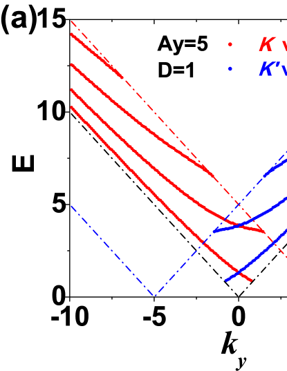
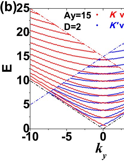
The GH effect is found when there is total internal reflection, and thus there are bound states localized in the channel between the two interfaces as shown in Figs. 3(a) and 3(b). The bound states exist only in the region between the curves given by the equations and , i.e., the transmission gap as we discussed above. The spectrum of each valley ( or ) alone is asymmetric, but for both valleys ( and ), the total spectra are mirror symmetric with respect to the transverse wave vector , as required by time reversal symmetry. That is very different from bound states in a pure electric waveguide in graphene, where the bound states are valley-independent and always mirror symmetric with respect to . Beenakker The number of bound states increases with the strain-induced gauge filed . Three typical regions in the energy spectrum are found: i) , i.e., , the incident electrons from both valleys are always totally reflected at the interfaces. The bound states for - or -valley electrons coexist for all incident angles. The electrons in different valleys have different group velocities determined by the slope of the energy dispersion relation. Thus such a waveguide may be used to separate the electrons in different valleys after passing a sufficient long channel. Notice that there are several local minima in the dispersion relation indicating a vanishing group velocity. Thus electrons in or valley will be trapped in the waveguide, which can be used to construct a valley memory device. ii) , i.e., , the incident electrons from both valleys are confined in the channel for incident angles . The transmission in such an angular window is similar to that in situation i). For (or ), only the bound states for valley (or valley) electrons appear, while electrons in valley (or valley) are able to penetrate into the strained region and eventually disappear from the channel region. So we can produce a valley-polarized current in such a strain-induced waveguide. iii) , i.e., . In this case, there is no coexistence of bound states for or valley. The transmission properties are similar as that in case ii) for and . Note that this valley-dependent transport property can not be realized in normal electric/magnetic waveguides proposed in previous works (see Refs. Chen ; Beenakker ).
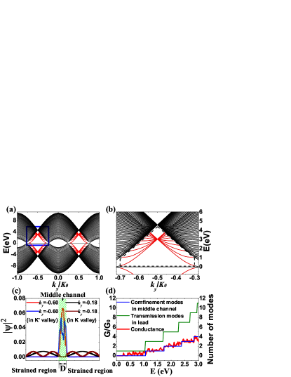
Finally, we focus on how the valley-polarized transmission features shown above are reflected in the conductance . Recently, Williams et al. Williams reported fiber-optic guiding of electrons in graphene. Differential resistance can be measured using a standard lock-in technique and thus guiding efficiency can be extracted. Our proposal depicted in Fig. 1 is a valley-related version of their setup. Here the guiding modes serve as valley-filtered modes while the bulk modes are unpolarized. To distinguish these valley-filtered modes from bulk modes, a higher guiding efficiency is desired. High guiding efficiency can be achieved by applying a uniform magnetic field as reported in Ref. Williams . But in this letter we propose a different scheme, where an applied mechanical strain behaves like a delta-function-like pseudomagnetic field, with opposite direction at the and valleys. We performed numerical simulations of electrical conduction in a tight-binding model ZZZhang of a strained graphene stripe. The dispersion relation is plotted in Figs. 4(a) and 4(b). The guiding modes are formed in the interval of the bulk states as shown in the dashed pentagon in Fig. 4(b). Note that when eV, all the forward-going guiding modes are located in valley, while the forwarding-going modes in valley are solely bulk modes. The density distributions of electrons in the lowest two forward-going modes in and valleys are shown in Fig. 4(c). Electron guiding modes (in valley) and bulk modes (in valley) are separated spatially in the channel and the strained region, respectively. The conductance shows good correspondence with the number of guiding modes rather than the much larger number of transmission modes in the leads [see Fig. 4(d)]. This is because electrons in bulk modes in the lead leak out of the channel and eventually disappear together with those in bulk modes in the strained region via the electric grounds G1 and G2. The reason for the oscillation of the conductance is that the stripe has a finite width and some bulk modes in the strained region still affect the conductance. One would expect that the conductance will approach the guiding mode steps very well when the strained region are electrical grounded. The guiding modes can effectively carry current from the injector I to the collector C and thus dominate the channel conductance. As we demonstrated that the guiding modes are valley-filtered, the desired valley polarized current can be measured in collector C. A valley detector as proposed in Ref. Zhai can be connected to the contact C to identify the polarization. The detector shows a large valley-resistance ratio, in analogy to the giant magnetoresistance effect. Thus valley polarized current could be identified by measuring the conductance at terminal C2.
In summary, We demonstrated theoretically how a strain-induced gauge field can be tailored to generate valley-polarized transport in a single layer of graphene. Our results show that the propagating behavior of electrons in graphene exhibits deep analogies with light as a consequence of the massless linear Dirac dispersion and the chirality of electron states. Most importantly, the gauge fields induced by strain can lead to valley-dependent transport phenomena, e.g., the Brewster angles and the Goos-Hänchen effect. Electrons in a waveguide structure formed by two strained stripes propagate along the channel with different velocities at different valleys. This feature shed new light on constructing graphene-based valleytronic device by using only strain, without the need for any external fields.
This work was supported by the NSF of China, the Swedish International Development Cooperation Agency (SIDA), and the Belgian Science Policy (IAP).
References
- (1) K. S. Novoselov, et al., Science 306, 666 (2004).
- (2) Y. Zhang, et al., Nature 438, 201 (2005).
- (3) A. H. Castro Neto, et al., Rev. Mod. Phys. 81, 109 (2009), and the references there in.
- (4) V. V. Cheianov, V. Fal’ko, and B. L. Altshuler, Science 315, 1252 (2007).
- (5) B. Özyilmaz, et al., Phys. Rev. Lett. 99, 166804 (2007).
- (6) S. V. Morozov, et al., Phys. Rev. Lett. 100, 016602 (2008).
- (7) C. H. Park, et al., Nano Lett. 8, 2920 (2008).
- (8) P. Darancet, V. Olevano, and D. Mayou, Phys. Rev. Lett. 102, 136803 (2009).
- (9) F. Goos and H. Hänchen, Ann. Phys. 436, 333 (1947).
- (10) C. W. J. Beenakker, et al., Phys. Rev. Lett. 102, 146804 (2009).
- (11) X. Chen, C. F. Li, and Y. Ban, Phys. Rev. B 77, 073307 (2008).
- (12) A. Concha and Z. Teanovi, Phys. Rev. B 82, 033413 (2010).
- (13) S. Ghosh and M. Sharma, J. Phys.: Condens. Matter 21, 292204 (2009).
- (14) L. Zhao, and S. F. Yelin, Phys. Rev. B 81, 115441 (2010).
- (15) J. R. Williams, et al., Nature Nanotech. advance online publication (13 February 2011).
- (16) D. Xiao, W. Yao, and Q. Niu, Phys. Rev. Lett. 99, 236809 (2007).
- (17) V. M. Pereira and A. H. Castro Neto, Phys. Rev. Lett. 103, 046801 (2009).
- (18) A. Rycerz, J. Tworzydo, and C. W. J. Beenakker, Nature Phys. 3, 172 (2007).
- (19) Z. Z. Zhang, K. Chang, and K. S. Chan Appl. Phys. Lett. 93, 062106 (2008).
- (20) J. M. Pereira, et al., J. Phys.: Condens. Matter 21, 045301 (2009).
- (21) D. S. L. Abergel and T. Chakraborty, Appl. Phys. Lett. 95, 062107 (2009).
- (22) F. Zhai, et al., Phys. Rev. B 82, 115442 (2010).
- (23) W. Z. Bao, et al., Nature Nanotech. 4, 562 (2010)
- (24) F. Guinea, M. I. Katsnelson, and A. K. Geim, Natue Phys. 6, 30 (2010)