A Biasing and Demodulation System
for Kilopixel TES Bolometer Arrays
Abstract
We describe the signal-processing logic, firmware, and software for a frequency-domain multiplexed (FDM) biasing and demodulation system that reads out Transition Edge Sensor (TES) bolometer arrays for mm-wavelength cosmology telescopes. This system replaces a mixed-signal readout backend with a much smaller, more power-efficient system relying on Field-Programmable Gate Arrays (FPGAs) for control, computation and signal processing. The new system is sufficiently robust, automated, and power efficient to be flown on stratospheric balloon-borne telescopes and is being further developed for satellite applications.
Index Terms:
Field-Programmable Gate Arrays (FPGAs), Digital Up/Down Converters, Digital Signal Processing (DSP)I Introduction
Large arrays of Transition Edge Sensor (TES) bolometers have recently seen widespread application to dark matter detection experiments and astronomical telescopes in the millimeter, sub-millimeter, far-infrared, soft x-ray, and gamma-ray bands (see, for example, [1, 2, 3, 4, 5, 6, 7, 8]). This is due to their exquisite sensitivity for incoherent detection, ease for fabrication of large monolithic arrays using photolithographic techniques, and relative insensitivity to microphonics due to their low impedance. The detector arrays typically operate at sub-Kelvin temperatures, so the thermal load presented by the wires connecting cryogenic hardware to room-temperature electronics is a significant design constraint. In such situations, it is desirable to multiplex many signals onto a reduced number of wires, using, for example, time-domain multiplexing [9] (TDM) or frequency-domain multiplexing (FDM) [10, 11].
In this paper, we describe the logic and firmware design of the Digital Frequency-domain Multiplexer (DFMUX), a power- and space-efficient FDM system that multiplexes up to 16 TES bolometers on a single readout module consisting of one set of wires entering the cryostat. Each module uses a single series array Superconducting Quantum Interference Device (SQUID) [12] operating at as a transimpedance pre-amplifier. This readout system is being used for several mm-wavelength telescopes including the EBEX Balloon-borne polarimeter [3] and POLARBEAR experiment [13].
The FDM modulator and demodulator logic for each readout module is implemented on a Xilinx Virtex-4 FPGA [14]. In addition to a high channel density on each set of wires, this system achieves a high overall density, supporting 4 multiplexed readout modules on a single 6U VME circuit board with one FPGA; up to 20 such cards have been operated in a single VME subrack. Where multiple subracks are used, clock and timing signals are daisy-chained between them.
The DFMUX is intended to supersede a mixed-signal system described in [10, 15, 4] with a system that is sufficiently small and power-efficient for balloon-borne experiments. An overview may be found in [11], with a description of an early system design. The high-level software control of the system, along with its use to tune the cryogenic electronics, is documented in [16]. In this paper, we focus on a system-level description and analysis of the DFMUX signal path, and highlight recent changes that extend the design, improve channel density, and increase performance in the noise environment exhibited in the field. We begin by describing the system’s basic operation in Section II. We focus on the digital signal path in Section III. We then examine the firmware and on-board software in Section IV. We explore the system performance in Section V and conclude with Section VI.
II System Description
Figure 1 shows a simplified diagram of a FDM bolometer readout system. The goal of such a system is to minimize the number of wires crossing into the cryostat by multiplexing several bolometer signals on a single set of wires, without degrading each bolometer’s noise performance. Multiplexing is desirable since the thermal load presented by wires entering the cryostat is substantial. Cryogenic refrigeration consumes a significant fraction of an experiment’s power budget, and cryogenic fridge cycling is time-consuming enough to impact the experiment’s uptime.
This system synthesizes a set of carrier combs, which enter the cryostat on a single wire. Each of these combs is selected by a corresponding bandpass filter and passes through a bolometer, which imposes a gain proportional to its incoming photon flux. This time-varying gain modulates each carrier frequency, producing sidebands. Each bolometer’s band-limited output is summed together to form the modulated sky signal.
The modulated sky signal is of very low power, and must be amplified before being passed to room-temperature electronics. To do so, we use a Semiconductor Quantum Interference Device (SQUID). SQUIDs may be used as extremely sensitive transimpedance amplifiers, but are only approximately linear in a limited dynamic range. To minimize harmonic distortion, we operate the SQUID in a negative feedback loop. In addition, we remove the residual carrier signals via destructive interference using a nuller comb.
Finally, the nulled sky signal is passed back to room-temperature electronics for demodulation. Each channel is demodulated to baseband, low-pass filtered, and archived for analysis.
Our design has much in common with the digital up- and down-converters (DUC and DDC, respectively) used in GSM and other multichannel base-station applications [17, 18]. However, the DFMUX differs from traditional DUC and DDC implementations in several crucial ways:
-
•
Our bandwidth for each channel is relatively small (10s of Hz). Since the modulator sinusoid is used to both electrically bias the TES and carry the ultra-low noise signals, the dynamic range requirement of is extreme. We require no degradation of noise performance down to several 10s of mHz.
-
•
The modulator generates only combs of carrier sinusoids. The modulation process itself takes place inside the cryogenic vessel.
-
•
Both the modulator and demodulator for each channel reside on the same FPGA. This means, for example, that each channel’s modulator and demodulator need only be synchronized once since their clocks cannot drift with respect to each other. Clock jitter cancels and is not a significant source of low-frequency noise.
-
•
In addition to its readout and tuning roles, the DFMUX is also used as a real-time bench instrument. Thus, it is desirable to have flexible control and a readily understandable signal path. This motivates features that are used occasionally, such as input re-routing and debugging facilities.
-
•
The system must be robust against crashes causing interruptions in the detector biases since this can necessitate thermal cycling of the sensors, requiring re-initialization of cryogenic systems. This can take about an hour per comb, adversely affecting the observing efficiency of the telescope applications.
III Signal Path
In this section, we describe the signal path for each detector channel during ordinary operation. Fig. 2 shows a schematic including a single readout module.111 Fig. 2 has been simplified. It neglects, for example, details of the differential signaling scheme and a separate board containing additional amplifiers (the “SQUID controller” board.) For details of the warm and cold electronics beyond the DFMUX, readers are referred to [19, 20]. At a channel’s resonant frequency, its LC filter has negligible impedance, permitting current to flow through the associated bolometer (modeled here as a resistance that varies with incoming optical power.) Although crosstalk from adjacent channels is nonzero, it may be controlled by selecting a set of resonant frequencies with adequate spacing.
Each DFMUX consists of a motherboard, shown on the left side of Fig. 2, and up to two mezzanines. Each mezzanine contains the analog electronics for two of the DFMUX’s four modules, including 16-bit Digital-to-Analog Converters (DACs) and 14-bit Analog-to-Digital Converters (ADCs) operating at 25 MSPS. Each mezzanine also houses analog anti-aliasing filters at both DAC outputs and ADC inputs, as well as a sequence of amplifiers with programmable gains. The room-temperature backend electronics presently supports up to 16 multiplexed TESes per module. Instruments that are presently operating have just 8 TESes wired together per module; upgrades to a larger channel count are in progress.
The conversion between ADC and DAC units and physical quantities are summarized in Table I. Voltages are measured at the mezzanine connectors (i.e. , , and shown in Fig. 2), and assuming matched load resistances. The post-ADC signal chain in the DMFD involves other conversion factors that are examined below; these factors are not present in Table I.
DMFS DMFD Setting PGA DAC Scale PGA ADC Scale Gain () Gain () Low 0.48 0.99 Med. Low 1.09 4.76 Med. High 3.33 33.3 High 10 100
The carrier DAC generates a weighted sum of sinusoids. Each sinusoidal component is tuned to match the resonant frequency of an LC filter in the cryostat associated with a single bolometer, with an amplitude chosen to provide the necessary voltage bias for the TES. The tuning procedures used to optimize the bias voltages and currents for the detectors and SQUIDs are described in [16]. The resistance of each bolometer (and thus the current through it) varies in response to sky signals, amplitude modulating the sinusoidal carrier. As a result, each bolometer adds sidebands around its carrier frequency with a typical signal bandwidth of .
Currents from all bolometers are summed at the input inductor of the SQUID. A second (nuller) DAC generates a second weighted sum of sinusoids that is injected at the SQUID input. The phase and amplitude of these sinusoids are adjusted to cancel the carrier signals in order to reduce the dynamic range requirements of the SQUID. Were nulling perfect, the current through the SQUID-coupled input inductor would consist only of the sidebands from each bolometer. In reality, some amount of carrier power remains. The SQUID is operated in a flux-locked loop with shunt feedback [21]. It converts current through its input inductor to a voltage signal at its output. This signal is amplified, filtered to limit aliasing during sampling, digitized by the ADC, and sent to the FPGA for demodulation.
In the following sections, we describe the structures within the FPGA that perform each of the biasing and readout functions. We refer to the signal path performing carrier synthesis as the Digital Multi-Frequency Synthesizer (DMFS) and the demodulation signal path as the Digital Multi-Frequency Demodulator (DMFD).
III-A Digital Multi-Frequency Synthesizer (DMFS)
III-A1 Structure
Each of the four modules in a DFMUX is associated with two identical DMFS blocks. One generates the carrier signals that bias bolometers. The other DMFS generates the nuller signals that cancel out these carriers at the SQUID input. These blocks synthesize waveforms for one wire at 25 MSPS. DMFSes operate independently and are not synchronized (meaning that the fixed phase between any two DMFS channels set to the same frequency cannot be determined without measurement.) The schematic for a single DMFS block is shown in Fig. 3.
Each of the 16 sinusoids in an individual DMFS block are generated using vendor-supplied [22], 12-bit, 2’s-complement Direct Digital Synthesizers (DDSes) as shown in Fig. 3. To maximize design density, each DDS generates sinusoids for 8 channels and operates at an internal clock rate of 200 MHz. Each DDS uses a 32-bit phase accumulator to track the waveform’s phase. Each clock cycle this accumulator is incremented, truncated to 14 bits, then used to reference the address of the waveform’s amplitude in a look-up table. A separate 32 bit register provides a programmable phase offset. When operating at 25 MHz, the frequency can be specified to 0.006 Hz. The spurious free dynamic range (SFDR) is 96 dB. This algorithm does not use substantial logic resources, but does use a significant number of the FPGA’s block RAM (BRAM) structures. Since each DDS block synthesizes 8 sinusoids, two such DDSes are required for each 16-channel module.
After synthesis by a DDS, each channel’s sinusoid is then weighted by a 20-bit 2’s-complement amplitude. This weighting is used to allow Joule heating provided by the voltage bias to be individually controlled. This allows each bolometer, which can have significantly different device parameters due to fabrication process variability, to be tuned to its optimum bias point. Each weighted sinusoid is then summed with the other 15 channels in its DMFS, and truncated to form a 16-bit signal for the associated DAC. The signal from each DMFS is finally converted from 2’s-complement to a positive binary number and passed to the 25 MHz clock domain for digital-to-analog conversion.
The slight DC bias resulting from truncation in the DMFS is unimportant since carrier and nuller outputs are AC-coupled.
III-B Digital Multi-Frequency Demodulator (DMFD)
Signal processing within the DMFD is illustrated in Fig. 4.
III-B1 Routing
The DMFD simultaneously demodulates input signals from four readout modules, each sampled at 25 MSPS. These inputs generally correspond to each of the DFMUX’s four 14-bit ADCs. For debugging and biasing duties, it also is possible to reroute the four inputs directly to the DMFS signals, bypassing A/D and D/A conversion entirely. (This routing capability has been used, for example, to use the DFMUX as a network-analysis tool, comparing the phase shift and attenuation caused by an analog circuit to a reference sinusoid that has been rerouted from the DMFS directly into a separate DMFD.)
III-B2 Downconversion
Once each signal has been routed for demodulation, it is mixed with 17 real reference waveforms to produce baseband signals. The frequency and phase of the reference waveforms can be programmed independently. The number of demodulators is one greater than the number of multiplexed detector channels. The 17th channel is identical to the other 16, but is not otherwise committed to a bolometer and is thus free to be placed in quadrature with another channel’s demodulator to form a complex (IQ) demodulator. A complex demodulator is helpful during tuning and testing, but is not necessary during ordinary readout.
Waveforms generated within the DMFD are equivalent to coarsely quantized sinusoids. These waveforms are synthesized with a custom DDS that uses samples of a length-16 sequence addressed with a phase accumulator at the desired frequency. The frequency spectra of references generated in this manner are tractable but complicated [23, 24], and are suitably approximated by that of ideal sinusoids for our purposes. The sequence is symmetric; a positive half-cycle is . The RMS amplitude of waveforms synthesized using this sequence is approximately , or about 4% lower than the ideal sinusoid’s RMS of . The synthesizer’s SNR is frequency-dependent. Vendor-supplied DDSes are not used for downconversion in the DMFD due to limited FPGA resources, and because the available DDSes do not permit phase synchronization between channels.
In order to permit quadrature demodulation, waveforms synthesized in the DMFD may be phase locked. Each synthesizer’s instantaneous phase may be placed on a bus, and other synthesizers may load it if instructed. This process allows any two channels in the DMFD to be phase-locked with a fixed, programmable phase offset between them. It is typically used to construct quadrature demodulators using the 17th DMFD channel mentioned above. While this implementation does require that all channels share a phase bus, it does so at modest cost in terms of FPGA resources, and uses vastly fewer resources than producing quadrature outputs for each channel.
III-B3 Decimation
After mixing, each channel within the DMFD contains a demodulated signal at baseband, sampled at 25 MSPS. Since the bandwidth of interest is a tiny fraction of the full Nyquist bandwidth, and since this sampling rate presents practical difficulties for streaming and storage, it is desirable to decimate these signals by a large factor (). The remainder of the DMFD is largely devoted to performing this decimation efficiently.
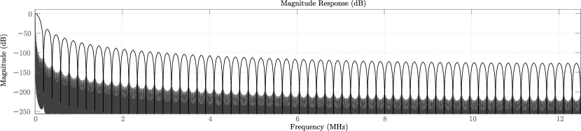
Each channel is first processed by its own Cascaded Integrator-Comb (CIC) decimation filter [25], labelled CIC1 in Fig. 4. CIC decimators are constructed using only accumulators and adders, which map very naturally to the resources available on an FPGA. However, since CICs exhibit significant passband nonlinarity and have broad transition regions, they are generally followed by compensating FIRs to restore uniform gain and perform additional decimation. The first-stage CIC reduces the overall sampling rate by a factor of 128, has 3 stages, and uses 35 bits internally. CIC1 output is then truncated to 17 bits.
After the CIC1 filter, all 68 channels are multiplexed onto a shared data bus. Hereafter, all filters are time-multiplexed and operate on each channel in sequence for a substantial savings in FPGA resources.
Following this multiplexer, a second CIC filter (CIC2) decimates by a further factor of 16. CIC2 uses four stages using 33-bit internal signals. After CIC2, each channel has a data rate of and is truncated to 17 bits.
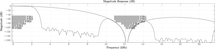
Filter Decimation Taps Output Signal Factor Rate Bandwidth CIC1 128 - 195.3 k Hz CIC2 16 - 12.21 k Hz FIR1 2 43 6103 Hz FIR2 2 108 3051 Hz FIR3 2 108 1526 Hz FIR4 2 108 762.9 Hz FIR5 2 108 381.5 Hz FIR6 2 108 190.7 Hz
The signals are then processed by a sequence of Finite Impulse Response (FIR) filters [26]. The first FIR includes correction for amplitude distortion introduced by the CIC filtering stages, and is 43 taps in length. The second through sixth FIRs are identical, unit-gain, 108-tap filters with unit passband gain. Although it would be computationally more efficient to optimize each FIR individually, using the same FIR prototype for each of the DMFD’s possible outputs provides a consistent and predictable output scale at a variety of sampling rates. This consistency is particularly desirable since switching between FIRs is only typically used during debugging, when it is sometimes necessary to view the baseband signal with greater bandwidth than is provided by normal readout (which typically occurs at FIR5 or FIR6.) The DMFD’s decimation stages are summarized in Table II. Each filter’s accumulator width is large enough to avoid overflow. Output is truncated to 17 bits.
The system’s baseband spectral response is shown after CIC1, CIC2, and FIR1 in Figures 5-6. The spectral response for filters FIR2 through FIR6, which are identical, is shown in Fig. 7.
III-B4 Buffering and MicroBlaze Interface
The user may instruct the DFMD to send data directly from any of the FIR stages to the output FIFO through a software-controlled multiplexer, such that the data rate and signal bandwidth can be varied. This makes the system immediately amenable to different detector bandwidths and to debugging and measuring detector properties. Each sample emerging from the selected FIR stage is truncated to a 24-bit 2’s-complement number and tagged with an 8-bit channel identifier. The resulting 32-bit data is timestamped and written into the data FIFO for retrieval by software.
We note that it is slightly redundant to store channel identifiers alongside channel data. We used this approach since the data FIFO will overflow and lose samples unless software is able to consume samples faster than they are produced. While this is not the case under ordinary operation, the FIFO does fill up during system boot or when data is not being streamed from the board; thus, software must be able to detect and recover from disordered data. This is easy to accomplish with channel identifiers, and the additional FIFO requirements are not onerous. (In future revisions, this problem may be avoided by delivering samples via either DMA or a so-called packet FIFO.)
In the next section, we describe a timestamping process occurring in tandem with the filtering described above. After decimation and timestamping, the aggregate data throughput is relatively low, and slight variations in signal delay are no longer problematic. Thus, we drain the FIFO under software control as described in Section IV-B.
III-B5 Timekeeping
The DFMUX system is used in several experiments, each of which uses different timekeeping standards and hardware. To integrate seamlessly with these experiments, a timestamp multiplexer system accepts timestamps from different timestamp units, including IRIG-B [27] (derived from an external GPS receiver) and an EBEX-specific [28] timing system generated by a separate timekeeping board.
Along with the format-specific timestamp decoders, we maintain local “ticks” counters. These counters are clocked by the DFMUX’s oscillator and reset whenever a new timestamp is decoded. They are used to increase the resolution of timestamps available to the DFMUX within each interval between external timestamps. They also permit the system to assign its own timestamps when no external timestamps are provided to the board.
In both cases, decoded timestamps are less than 96 bits in size. These timestamps fit into four 32-bit entries in the data FIFO, after reserving space for 8-bit channel identifiers as described above for channel data. Each timestamp format is assigned four distinct channel identifiers.
Timestamps are added after multiplexing as follows: when the first channel is emitted from the selected readout stage, the DMFD captures a timestamp of user-specified format from the timestamp multiplexer. After the last data channel has been stored in the FIFO, this captured timestamp is broken into four 24-bit numbers, tagged with the selected format’s four assigned channel identifiers, and placed into the FIFO.
Since timestamps are captured and associated with data after the decimation process, the processing delays introduced by CICs and FIRs must be subtracted from the timestamps to refer data back to the instant it were sampled. This correction occurs in analysis software, since the timestamp format is opaque to the DFMUX itself.
IV Firmware and Software
From a user’s perspective, the high-level control of the DFMUX is described in [16]. In this section, we describe how the system is designed to present a straightforward, flexible interface for real-time use and automated control algorithms.
IV-A Control
Control instructions and queries are encoded as HTTP requests and received via the board’s Ethernet interface. They are decoded by a MicroBlaze processor running the linux kernel. Providing the HTTP interface are two webservers: a fully-featured, third-party webserver that serves a browser-accessible interface, and a fastpath used only for rapid interaction with hardware.
Although the HTTP interface allows all aspects of the DFMUX to be controlled, it is a low-level interface that does not provide a method of interacting with data from the signal path. To perform higher-level, possibly data-dependent interactions (such as tuning the board), we provide a port of the Python scripting environment, with a hardware-interface library that permits scripts to control device registers directly. A Python library, pyWTL, supplies higher-level interactions and allows board-level control to be performed in a consistent, network-transparent manner, regardless of whether it runs on a DFMUX or a PC.
Developing the higher-level code in an user-friendly environment like Python, and allowing this code to run on either the DFMUX or a PC, permits physicists as well as engineers to contribute to the development process.
IV-B Data Streaming
In Sections III and IV, we described the signal path and its control. In the following section, we discuss how data is removed from the FIFO, packaged, and streamed across the network for storage.
Depending on which FIR stage has been selected, data from each channel is streamed into the FIFO at a rate between and , for an aggregate throughput of between and including timestamps. Data are removed from the FIFO in frames (sets containing one sample from each user-selected channel and a single timestamp), and wrapped into packets containing several frames. The number of frames per packet is chosen to maximize network throughput, i.e. to maximize the size of each packet without causing fragmentation at the network layer.
Once a packet is constructed, it is sent via unicast or multicast UDP to a network address controlled by the Python or web interfaces. Since UDP does not guarantee data transmission, network topology and hardware have been carefully tested to ensure minimal packet loss. (Although TCP would permit retransmission of dropped packets, a TCP-based transport would not permit multicasting. It is also not clear, at expected data rates, that the MicroBlaze and network hardware have the capacity to recover without further packet losses.)
Packets are received by a companion utility (the “parser”) and a Python interface. The parser streams data to disk for both real-time monitoring using KST [29] and off-line analysis. Using SWIG [30], the Python interface integrates seamlessly with the pyWTL module described above and is used for on-line tuning, control, and analysis tasks.
V System Performance
V-A DMFS Noise
There are three general classifications of noise in the DMFS: digital noise, DAC noise, and analog noise. In this section, we quantify each of these noise sources and determine the dominant source.
There are two sources of digital noise: that intrinsic to the DDS algorithm, and quantization noise from the system’s finite bit length. We model both of these noises as additive uniform white noise, independent from other noise sources. The noises thus add incoherently, and we may determine an overall noise figure for the digital portion of the DMFS. Digital noise is summarized in Table III. The overall RMS noise is approximately 1.16 LSBs at the DAC. This corresponds to a PSD of at the DAC.
Noise Source RMS Noise (DAC LSBs) Per Channel Total DDS Truncation Total
The vendor documentation for the DAC suggests approximately SFDR in our operating regime. If we model this as a white-noise floor, the corresponding RMS noise is 1.65 DAC LSBs, slightly dominating the digital noise. In terms of volts at the DAC, this corresponds to .
Noise in the DMFS’s analog circuitry is dominated by its first-stage amplifier, which has an input-referred noise of .
Thus, the dominant source of noise in the modulator is the DAC itself, followed by quantization noise in the digital portion of the system. The overall noise is approximately at the DAC. Referred to an equivalent voltage at the DMFS’ output (assuming an load), the modulator’s noise performance is summarized in Table IV.
DMFS Gain Noise Setting Gain () Low 0.48 Med. Low 1.09 Med. High 3.33 High 10.0
V-B DMFD Noise
In the DMFD, as in the DMFS, there are three general sources of noise: noise in the analog circuitry, noise in the analog-to-digital converter (ADC), and noise in the digital signal chain. In this section, we examine these noise sources and determine the overall performance of the demodulator.
Neglecting the source signal, noise in the analog signal chain is dominated by the first amplification stage. These amplifiers have an input-referred noise of .
The ADC exhibits a SNDR (signal to noise-plus-distortion ratio) of , or at the ADC () at a sampling rate of 25 MSPS, assuming a full-scale sinusoidal input signal.
Noise in the digital chain is dominated by mixer effects and truncation. Each of these noise sources are evaluated in this section. (We neglect noise from aliasing in the decimation filter chain, as it is subdominant.)
Because it is a nonlinear device, the mixer alters properties of noise in its input. The mixer also contains a truncation stage, injecting noise of its own after mixing. As noted above, the mixer’s performance depends on the particular carrier frequency chosen, but its response to a Gaussian white noise input with RMS amplitude is readily approximated as a white-noise output with RMS amplitude . (The factor is the RMS of the mixer’s coefficients; an ideal sinusoidal mixer would amplify noise by a factor of ) The distortion added by the mixer’s truncation stage may be modeled as additive uniform white noise of RMS amplitude post-mixer LSBs/ following the mixer, or streamer LSBs/.
To determine the overall noise level in the DMFD, we refer each source of noise both back to the DMFD input (so it may be compared to physical signal levels) and to the DMFD’s streamed output (so it may be compared to measurements.) These noise levels are summarized in Table V.
Noise Source Intrinsic DMFD Noise LSBs/ Low Gain (0.99) Analog ADC Digital Total Med. Low Gain (4.76) Analog ADC Digital Total Med. High Gain (33.3) Analog ADC Digital Total High Gain (100) Analog ADC Digital Total
Once again, the use of truncation instead of convergent rounding throughout the DMFD presents itself as a slight DC offset. For our applications, the detectors are capable only of measuring the difference signal between sky pointings, so no information is present at DC. Since any offset is discarded during analysis, we make no attempt to correct for additional bias introduced by truncation.
V-C Power Consumption
Because its intended uses include balloon-based experiments such as EBEX, the DFMUX’s power consumption is a crucial performance measure. In EBEX, the DFMUX is powered using (heavy) batteries. In addition, any heat generated by the electronics must be removed from the gondola. This is a non-trivial challenge task at high altitudes where the atmosphere is thin.
The DFMUX’s power profile is shown in Table VI. The first row shows consumption for the DFMUX’s digital circuitry only; the second includes two analog mezzanines, which include the DACs, analog signal path, and ADCs. Neglected in this power profile is the SQUID controllers, which are separate boards that sit between the DFMUXes and the cryostat. (SQUID controllers consume approximately each. One SQUID controller is required for every 2 DFMUXes.)
Scenario Voltage Current Power Motherboard Only With Mezzanines
Because FPGAs are not ordinarily considered power-efficient, we contrast the DFMUX’s power dissipation per bolometer channel relative to the analog fMUX, the mixed-signal implementation it supersedes. The analog fMUX [10, 15, 4] is currently deployed at the South Pole Telescope, and supports 840 electrically active bolometers with 60 boards. Each board includes 2 modules, each of which can support 7 bolometers. Overall, SPT’s analog fMUX crates draw , for a power consumption per bolometer of . In a digital fMUX system using a multiplexing factor of 16, power consumption per bolometer is , for an overall power savings in excess of 90%.
V-D FPGA Usage
The FPGA resources used by the design are summarized in Table VII. The capacities listed are for the Virtex-4 LX160 FPGA, which is used on all but a handful of our boards. Resource utilization is summarized for the signal path only, and for the entire design. The signal path figures comprise the DMFS and DMFD, but neither the timestamp decoders nor the FIFO connecting the DMFD to the processor bus. (The timestamp decoders are relatively small; the FIFO consumes approximately 30 additional RAMB16s.) The entire design includes the signal path, timestamp decoders, FIFOs, MicroBlaze, network and memory interfaces, plus interfaces for the on- and off-board peripherals and interfaces (voltage and temperature monitors, serial ports, etc.) supported by the DFMUX.
Resource Number Device Percent Type Used Capacity Used Signal Path Only DSP48 33 96 34% RAMB16s 85 288 29% Slices 31,459 67,584 46% Entire Design DSP48 56 96 58% RAMB16s 273 288 94% Slices 48,023 67,584 71%
VI Discussion and Future Work
We have described the signal path, control logic, and firmware of a highly-integrated FDM system for TES bolometers. This system is physically much smaller and less power-hungry than the mixed-signal system it replaces.
Because the bulk of the DFMUX’s signal processing is performed on a FPGA which may be easily reconfigured, the system has also found use in unexpected ways. With only trivial hardware modifications, a DFMUX was used to measure the surface accuracy of the South Pole Telescope’s secondary mirror [31]. A similarly modified DFMUX is used to measure the angular position of a rotating optical element (half-wave plate) in the EBEX telescope.
We are currently focusing on three improvements to the DFMUX. The first is an attempt to reduce its power requirements (per bolometer channel) by improving the design of its signal path. The second goal is to increase the number of bolometers multiplexed via each FDM module. We anticipate doubling or quadrupling the total number of bolometers per DFMUX by simply scaling the current design. Even greater channel densities may be achieved using polyphase filter banks [32] or similar techniques. Finally, we are investigating alternative biasing and feedback strategies that permit greater increases in channel density.
VII Acknowledgements
This work was supported by the Natural Sciences and Engineering Research Council of Canada (NSERC), the Canadian Institute for Advance Research and the Canada Research Chairs program. We also gratefully acknowledge hardware and software contributions from the Xilinx University Program. MD acknowledges Sloan Fellowship funding.
References
- [1] B. Cabrera, R. Clarke, A. Miller, S. W. Nam, R. Romani, T. Saab, and B. Young, “Cryogenic detectors based on superconducting transition-edge sensors for time-energy-resolved single-photon counters and for dark matter searches,” Physica B Condensed Matter, vol. 280, pp. 509–514, May 2000.
- [2] D. Schwan et. al. (The APEX-SZ Collaboration), “The APEX-SZ Instrument,” Review of Scientific Instruments, 2010.
- [3] W. Grainger, A. M. Aboobaker, P. Ade, F. Aubin, C. Baccigalupi, É. Bissonnette, J. Borrill, M. Dobbs, S. Hanany, C. Hogen-Chin, J. Hubmayr, A. Jaffe, B. Johnson, T. Jones, J. Klein, A. Korotkov, S. Leach, A. Lee, L. Levinson, M. Limon, J. Macaluso, K. MacDermid, T. Matsumura, X. Meng, A. Miller, M. Milligan, E. Pascale, D. Polsgrove, N. Ponthieu, B. Reichborn-Kjennerud, T. Renbarger, I. Sagiv, F. Stivoli, R. Stompor, H. Tran, G. Tucker, J. Vinokurov, M. Zaldarriaga, and K. Zilic, “EBEX: the E and B Experiment,” in Society of Photo-Optical Instrumentation Engineers (SPIE) Conference Series, vol. 7020, Aug. 2008.
- [4] J. E. Carlstrom, P. A. R. Ade, K. A. Aird, B. A. Benson, L. E. Bleem, S. Busetti, C. L. Chang, E. Chauvin, H. Cho, T. M. Crawford, A. T. Crites, M. A. Dobbs, N. W. Halverson, S. Heimsath, W. L. Holzapfel, J. D. Hrubes, M. Joy, R. Keisler, T. M. Lanting, A. T. Lee, E. M. Leitch, J. Leong, W. Lu, M. Lueker, J. J. McMahon, J. Mehl, S. S. Meyer, J. J. Mohr, T. E. Montroy, S. Padin, T. Plagge, C. Pryke, J. E. Ruhl, K. K. Schaffer, D. Schwan, E. Shirokoff, H. G. Spieler, Z. Staniszewski, A. A. Stark, and K. V. J. D. Vieira, “The 10 Meter South Pole Telescope,” ArXiv e-prints, Jul. 2009.
- [5] W. Holland, M. MacIntosh, A. Fairley, D. Kelly, D. Montgomery, D. Gostick, E. Atad-Ettedgui, M. Ellis, I. Robson, M. Hollister, A. Woodcraft, P. Ade, I. Walker, K. Irwin, G. Hilton, W. Duncan, C. Reintsema, A. Walton, W. Parkes, C. Dunare, M. Fich, J. Kycia, M. Halpern, D. Scott, A. Gibb, J. Molnar, E. Chapin, D. Bintley, S. Craig, T. Chylek, T. Jenness, F. Economou, and G. Davis, “SCUBA-2: a 10,000-pixel submillimeter camera for the James Clerk Maxwell Telescope,” in Society of Photo-Optical Instrumentation Engineers (SPIE) Conference Series, vol. 6275, Jul. 2006.
- [6] P. De Korte, J. Anquita, X. Barcons, P. Bastia, J. Beyer, F. Briones, C. Blatt, M. Bruijin, J. Bussons, A. Camon, M. Ceballos, D. Drung, C. Enns, L. Fabrega, G. Fraser, F. Gatti, L. Gottardi, W. Hajdas, P. Helisto, I. Hepburn, J. Willem den Herder, H. Hoevers, Y. Ishisaki, M. Kiviranta, J. Van der Kuur, A. Mchedlishvili, K. Mitsuda, L. Piro, J. Sese, N. Yamasaki, and C. Whitford, “EURECA: European-Japanese Microcalorimeter Array,” J. Low Temp. Phys., vol. 151, no. 3–4, pp. 733–739, 2008.
- [7] P. Mauskopf, D. Morozov, D. Glowacka, D. Goldie, S. Withington, M. Bruijn, P. DeKorte, H. Hoevers, M. Ridder, J. Van Der Kuur, and J. Gao, “Development of transition edge superconducting bolometers for the SAFARI far-infrared spectrometer on the SPICA space-borne telescope,” in Society of Photo-Optical Instrumentation Engineers (SPIE) Conference Series, ser. Presented at the Society of Photo-Optical Instrumentation Engineers (SPIE) Conference, vol. 7020, Aug. 2008.
- [8] W. B. Doriese, J. N. Ullom, J. A. Beall, W. D. Duncan, L. Ferreira, G. C. Hilton, R. D. Horansky, K. D. Irwin, J. A. B. Mates, C. D. Reintsema, L. R. Vale, Y. Xu, B. L. Zink, M. W. Rabin, A. S. Hoover, C. R. Rudy, and D. T. Vo, “14-pixel, multiplexed array of gamma-ray microcalorimeters with 47 eV energy resolution at 103 keV,” Applied Physics Letters, vol. 90, no. 19, p. 193508, May 2007.
- [9] K. D. Irwin, “SQUID multiplexers for transition-edge sensors,” Physica C, vol. 368, pp. 203–210, Mar. 2002.
- [10] T. M. Lanting, H.-M. Cho, J. Clarke, W. L. Holzapfel, A. T. Lee, M. Lueker, P. L. Richards, M. A. Dobbs, H. Spieler, and A. Smith, “Frequency-domain multiplexed readout of transition-edge sensor arrays with a superconducting quantum interference device,” Applied Physics Letters, vol. 86, no. 11, p. 112511, Mar. 2005.
- [11] M. Dobbs, E. Bissonnette, and H. Spieler, “Digital frequency domain multiplexer for millimeter-wavelength telescopes,” IEEE Trans. Nucl. Sci., vol. 55, no. 1, pp. 21–26, Feb. 2008.
- [12] M. E. Huber, P. A. Neil, R. G. Benson, D. A. Burns, A. F. Corey, C. S. Flynn, Y. Kitaygorodskaya, O. Massihzadeh, J. M. Martinis, and G. C. Hilton, “DC SQUID Series Array Amplifiers with 120 MHz Bandwidth (Corrected),” IEEE Transactions on Applied Superconductivity, vol. 11(2), pp. 4048–4053, 2001.
- [13] A. T. Lee, H. Tran, P. Ade, K. Arnold, J. Borrill, M. A. Dobbs, J. Errard, N. Halverson, W. L. Holzapfel, J. Howard, A. Jaffe, B. Keating, Z. Kermish, E. Linder, N. Miller, M. Myers, A. Niarchou, H. Paar, C. Reichardt, H. Spieler, B. Steinbach, R. Stompor, C. Tucker, E. Quealy, P. L. Richards, and O. Zahn, “POLARBEAR: Ultra-high Energy Physics with Measurements of CMB Polarization,” in American Institute of Physics Conference Series, ser. American Institute of Physics Conference Series, vol. 1040, Aug. 2008, pp. 66–77.
- [14] Virtex-4 FPGA User Guide.
- [15] M. Dobbs, N. W. Halverston, P. A. R. Ade, K. Basu, A. Beelen, F. Bertoldi, C. Cohalan, H. M. Cho, R. Güsten, W. L. Holzapfel, Z. Kermish, R. Kneissl, A. Kovács, E. Kreysa, T. M. Lanting, A. T. Lee, M. Leuker, J. Mehl, K. M. Menten, D. Muders, M. Nord, T. Plagge, P. L. Richards, P. Schilke, D. Schwan, H. Spieler, A. Weiss, and M. White, “APEX-SZ first light and instrument status,” New Astronomy Reviews, vol. 50, pp. 960–968, 2006.
- [16] K. Macdermid, P. Hyland, F. Aubin, E. Bissonnette, M. Dobbs, J. Hubmayr, G. Smecher, and S. Warraich, “Tuning of kilopixel transition edge sensor bolometer arrays with a digital frequency multiplexed readout system,” in AIP Conf. Proc., vol. 1185, 2009, pp. 253–256.
- [17] R. Andraka, “High performance digital down-converters for FPGAs,” Xilinx Xcell, vol. 38, pp. 48–51, 2000.
- [18] B. Ogilvie and P. Pacheco, “Designing digital downconverters,” RF Design, pp. 38–46, May 2006.
- [19] F. Aubin, A. Aboobaker, P. Ade, C. Baccigalupi, C. Bao, J. Borrill, C. Cantalupo, D. Chapman, J. Didier, M. Dobbs, W. Grainger, S. Hanany, J. Hubmayr, P. Hyland, S. Hillbrand, A. Jaffe, B. Johnson, T. Jones, T. Kisner, J. Klein, A. Korotkov, S. Leach, A. lee, M. Limon, K. MacDermid, T. Matsumura, X. Meng, A. Miller, M. Milligan, D. Polsgrove, N. Ponthieu, K. Raach, B. Reichborn-Kjennerud, I. Sagiv, G. Smecher, H. Tran, G. Tucker, Y. Vinokurov, A. Yadav, M. Zaldarriaga, and K. Zilic, “First implementation of TES bolometer arrays with SQUID-based multiplexed readout on a balloon-borne platform,” in Society of Photo-Optical Instrumentation Engineers (SPIE) Conference Series, ser. Presented at the Society of Photo-Optical Instrumentation Engineers (SPIE) Conference, vol. 7741, Jul. 2010.
- [20] B. Reichborn-Kjennerud, A. M. Aboobaker, P. Ade, F. Aubin, C. Baccigalupi, C. Bao, J. Borrill, C. Cantalupo, D. Chapman, J. Didier, M. Dobbs, J. Grain, W. Grainger, S. Hanany, S. Hillbrand, J. Hubmayr, A. Jaffe, B. Johnson, T. Jones, T. Kisner, J. Klein, A. Korotkov, S. Leach, A. Lee, L. Levinson, M. Limon, K. MacDermid, T. Matsumura, X. Meng, A. Miller, M. Milligan, E. Pascale, D. Polsgrove, N. Ponthieu, K. Raach, I. Sagiv, G. Smecher, F. Stivoli, R. Stompor, H. Tran, M. Tristram, G. S. Tucker, Y. Vinokurov, A. Yadav, M. Zaldarriaga, and K. Zilic, “EBEX: A balloon-borne CMB polatization experiment,” in Society of Photo-Optical Instrumentation Engineers (SPIE) Conference Series, ser. Presented at the Society of Photo-Optical Instrumentation Engineers (SPIE) Conference, vol. 7741, Jul. 2010.
- [21] H. Spieler, “Frequency domain multiplexing for large scale bolometer arrays,” in Monterey Far-IR, Sub-mm and mm Detector Technology Workshop proceedings, J. Wolf, J. Farhoomand, and C. McCreight, Eds., 2002, pp. 243–249.
- [22] DDS Compiler v2.0, Xilinx, Inc., 2007.
- [23] Y.-C. Jenq, “Digital spectra of nonuniformly sampled signals: fundamentals and high-speed waveform digitizers,” IEEE Trans. Instrum. Meas., vol. 37, no. 2, pp. 245–251, Jun. 1988.
- [24] Y. C. Jenq, “Digital spectra of nonuniformly sampled signals. II. digital look-up tunable sinusoidal oscillators,” IEEE Trans. Instrum. Meas., vol. 37, no. 3, pp. 358–362, Sep. 1988.
- [25] E. Hogenauer, “An economical class of digital filters for decimation and interpolation,” IEEE Trans. Acoust., Speech, Signal Process., vol. 29, no. 2, pp. 155–162, Apr. 1981.
- [26] FIR Compiler v3.0, Xilinx, Inc., 2007.
- [27] IRIG Serial Time Code Formats, Telecommunications and Timing Group, Range Commanders Council Std., May 1998.
- [28] P. Oxley, P. Ade, C. Baccigalupi, P. deBernardis, H.-M. Cho, M. J. Devlin, S. Hanany, B. R. Johnson, T. Jones, A. T. Lee, T. Matsumura, A. D. Miller, M. Milligan, T. Renbarger, H. G. Spieler, R. Stompor, G. S. Tucker, and M. Zaldarriaga, “The EBEX experiment,” Proc. SPIE, vol. 5543, pp. 320–331, 2004.
- [29] D. Hanson, R. Chern, P. Rodrigues, B. Nettterfield, Y. Mao, and Z. Zhang, The KST Handbook, The University of British Columbia, The University of Toronto, 2009.
- [30] D. M. Beazley, SWIG User’s Manual, Dept. of CS, University of Utah, 1997.
- [31] S. Padin, Z. Staniszewski, R. Keisler, M. Joy, A. A. Stark, P. A. R. Ade, K. A. Aird, B. A. Benson, L. E. Bleem, J. E. Carlstrom, C. L. Chang, T. M. Crawford, A. T. Crites, M. A. Dobbs, N. W. Halverson, S. Heimsath, R. E. Hills, W. L. Holzapfel, C. Lawrie, A. T. Lee, E. M. Leitch, J. Leong, W. Lu, M. Lueker, J. J. McMahon, S. S. Meyer, J. J. Mohr, T. E. Montroy, T. Plagge, C. Pryke, J. E. Ruhl, K. K. Schaffer, E. Shirokoff, H. G. Spieler, , and J. D. Vieira, “South pole telescope optics,” Applied Optics, vol. 47, pp. 4418–4428, 2008.
- [32] F. J. Harris, Multirate Signal Processing for Communication Systems. Prentice Hall, 2004.