Critical comparison of electrode models in density functional theory based quantum transport calculations
Abstract
We study the performance of two different electrode models in quantum transport calculations based on density functional theory: Parametrized Bethe lattices and quasi-one dimensional wires or nanowires. A detailed account of implementation details in both cases is given. From the systematic study of nanocontacts made of representative metallic elements, we can conclude that parametrized electrode models represent an excellent compromise between computational cost and electronic structure definition as long as the aim is to compare with experiments where the precise atomic structure of the electrodes is not relevant or defined with precision. The results obtained using parametrized Bethe lattices are essentially similar to the ones obtained with quasi one dimensional electrodes for large enough sections of these, adding a natural smearing to the transmission curves that mimics the true nature of polycrystalline electrodes. The latter are more demanding from the computational point of view, but present the advantage of expanding the range of applicability of transport calculations to situations where the electrodes have a well-defined atomic structure, as is case for carbon nanotubes, graphene nanoribbons or semiconducting nanowires. All the analysis is done with the help of codes developed by the authors which can be found in the quantum transport toolbox Alacant and are publicly available.
I Introduction
One of the most active research fields in Nanoscience is the one focusing on understanding and controlling the charge transport between bulk electrodes when these are connected by an atomic- or a molecular-size region and a bias voltage is applied between themAgraït et al. (2003), in other words, understanding and controlling the formation and concomittant resistance of nanoscopic bridges. More than 10 years of experimental along with theoretical work is finally taking us to an unprecedented level of control and comprehension of these systems. On the theoretical side, we have witnessed the marriage of theoretical quantum transport basics and density functional theory, giving birth to one of the most active and fructiferous fields in theoretical nanoscience Lang (1995); Di Ventra et al. (2000); Taylor et al. (2001); Palacios et al. (2001); Xue et al. (2001); Palacios et al. (2002); Brandbyge et al. (2002); Heurich et al. (2002); Ventra and Lang (2002); Palacios et al. (2003); Fujimoto and Hirose (2003); Louis et al. (2003); Xue and Ratner (2003a, b); Basch and Ratner (2003); Jelínek et al. (2003); Ke et al. (2004); Hirose et al. (2004); Xue and Ratner (2004); Liang et al. (2004); Rocha and Sanvito (2004); Frederiksen et al. (2004); Thygesen and Jacobsen (2005); Evers et al. (2004); Tada et al. (2004); Nara et al. (2004); Ferretti et al. (2005); Toher et al. (2005); Fujimoto et al. (2005); Asari et al. (2005); Wu et al. (2005); Choi et al. (2005); Ke et al. (2005a, b); Bagrets et al. (2006); Smogunov et al. (2006); Jiang et al. (2006); Havu et al. (2006); Hod et al. (2006); Rocha et al. (2006); Nakamura and Yamashita (2006); Prociuk et al. (2006); Mera et al. (2007); Mizuseki et al. (2007); Nakamura (2007); Qian et al. (2007); Thygesen and Rubio (2007); Pauly et al. (2008); Liu et al. (2008); Bernholc et al. (2008); Li et al. (2008a); Oetzel et al. (2008); Jelinek et al. (2008); Bredow et al. (2008); Hyldgaard (2008); Kondo et al. (2008); Li et al. (2008b); Mowbray et al. (2008); Smeu et al. (2008); Thygesen (2008); Yoshizawa et al. (2008); Zhao and Dunietz (2008); Garcia-Lekue and Wang (2009); Gutierrez et al. (2009); Lopez-Bezanilla et al. (2009); Wang and Guo (2009); Jacob et al. (2009).
For nanoscopic conductors every atom counts and the transport properties are strongly dependent on the detailed atomic arrangement. Thus, in order to make theoretical predictions that can be compared with experimental results, it is important, to have a reliable description of, first, the atomic structure of the conductor and, second, the accompanying electronic structure. This can be achieved most conveniently with the aid of ab initio electronic structure methods based on atomic orbitals such as, e.g., GaussianFrisch et al. (2003), CrystalDovesi et al. (2006) or SiestaOrdejón et al. (1996). These codes implement density functional theory (DFT) to obtain an effective mean-field description of the electronic structure of, in our case, the nanoscopic bridge. This is typically done through the effective Kohn-Sham one-body Hamiltonian that takes into account the electron-electron interactions at a static mean-field level.
A central challenge in the theoretical description of these systems is that the electronic structure of the atomic- or molecular-size conductor is altered by the coupling to the bulk electrodes. Thus, in calculating the electronic structure the coupling to the (semi-infinite) electrodes has to be taken into account. This poses the difficult problem of dealing with an infinite system without translation invariance. In addition, one should strictly carry out the electronic and atomic structure calculation out of equilibirum, as imposed by the applied voltage. This is usually done by making use of the one-body Green’s functions (GFs) and the so-called partitioning technique, as will be explained in the following sections.
Clearly, while the detailed atomic and electronic structure of the nanoscopic bridge plays a crucial role, farther away from the bridge these become less important. Besides, the exact atomic structure of the bulk electrodes, as encountered in real experiments, is not known and cannot be controlled with precision beyond a few contact atomsTrouwborst et al. (2008). This lack of control lies behind the statistical deviations observed in measurable quantitites such as the conductance. This brings us to the important question of how to model the bulk electrodes, mantaining a compromise between realism and computational effort. Several possibilities of how to model the electrodes have been presented in the literature, with every model having advantages and disadvantagesLang (1995); Palacios et al. (2001); Brandbyge et al. (2002); Heurich et al. (2002). Here we explore the use of two types of electrode models: (i) parametrized tight-binding (TB) Bethe latticesPalacios et al. (2001, 2002) and (ii) perfect nanowires of finite section, stressing their weaknesses and strengths as models to represent the reality. Another related question which we partially address in this paper is to what extent the particular shape or atomic arrangement of the electrodes near the bridge introduces variations in the conductance and how these depend on the chemical nature of the atoms. The results presented below are all obtained with codes developed by the authors over the years which can be found in the publicly available quantum transport toolbox ALACANTPalacios et al. .
II Non-equilibrium Green’s functions and Landauer formalisms
In the following, and for completeness’ sake, we give a summary of the central aspects to the non-equilibrium Green’s function (NEGF) and Landauer formalisms formulated for a non-orthogonal localized atomic basis set. Although most of the details can be found in the early literature Taylor et al. (2001); Palacios et al. (2001); Xue et al. (2001); Palacios et al. (2002); Brandbyge et al. (2002); Heurich et al. (2002); Louis et al. (2003); Xue and Ratner (2003a, b); Ke et al. (2004); Rocha and Sanvito (2004); Thygesen and Jacobsen (2005); Ferretti et al. (2005), here we discuss in depth some of those that are not usually addressed and become essential for a correct implementation of the above mentioned formalisms.
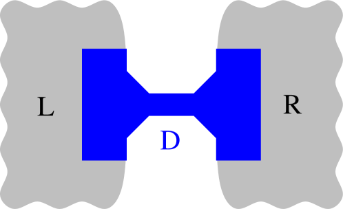
We divide the system into three parts, as shown in Fig. 1: The semi-infinite left (L) and right (R) electrodes or, hereon, leads, and the intermediate region between the two leads hereon called device (D) which contains the a central, narrow region where most of the scattering takes place (e.g., a nanoscopic constriction of the same material as the leads or a trapped molecule). We assume that the leads are only coupled to the scattering region but not to each other. In a localized atomic basis set the Hamiltonian of the system is given by:
| (1) |
Since atomic basis sets are usually non-orthogonal we also have to take into account the overlap between the atomic orbitals given by the matrix :
| (2) |
In order to deal with the problem of an infinite system without translation invariance, it is convenient to make use of the one-body Green’s functions as explained, e.g., in the book by EconomouEconomou (1970). The one-body Green’s function (GF) is defined as the resolvent operator of the one-body Schrödinger equation:
| (3) |
where is, in general, a complex number and is the identity.
If does not coincide with an eigenvalue of the Hamiltonian the GF operator has the following simple solution: .
Obviously, for the GF operator has a pole and is thus not well defined. In this case one can define two GFs by a limiting procedure: The retarded GF is defined as , and the advanced GF is defined as where is a real number (the energy). The retarded (advanced) GF can be analytically continued into the upper (lower) complex plane. Moreover, away from the poles of , i.e., for both definitions coincide with : .
Because of the non-orthogonality of the basis set it is convenient to define the following Green’s function matrix
| (4) |
Note that this Green’s function matrix is not the standard one which is simply defined by the matrix elements of the GF operator . However, the latter GF matrix is inconvenient to handle in the case of non-orthogonal basis sets (see Appendix A for a complete discussion).
Using the technique explained in App. B it can be shown that the GF of the device region is given by the following matrix:
| (5) |
where and are the so-called lead self-energies which describe the coupling of the device to the semi-infinite L and R leads. These self-energies can be calculated from the Green’s functions of the (isolated) leads, :
| (6) |
where the index denotes the electrode L or R, and we have exploited the hermiticity of the Hamiltonian and the overlap matrix, i.e., and .
All quantities of interest such as the density of states (DOS), charge density, current , and zero-bias as well as differential conductance can be calculated from the GF matrix of the device region and the lead self-energies and . For instance, in the case of an effective Kohn-Sham one-body Hamiltonian, as considered here, the current through the nanoscopic conductor is given by the famous Landauer formulaLandauer (1970):
| (7) |
where represents the Fermi distribution function, the left and right chemical potentials, and the transmission function, , can be calculated from the retarded and advanced GFs by the Caroli expressionCaroli et al. (1971):
| (8) |
Here and are the so-called coupling matrices which are defined as
| (9) | |||||
| (10) |
Note that, since the self-energy matrices are usually symmetric, the coupling matrices are just (twice) the imaginary parts of the self-energies.
At zero temperature the zero-bias conductance is now just given by the transmission function at the Fermi level (i.e. the electrochemical potential at zero temperature):
| (11) |
Hence, the transmission function is the central quantity for calculating the electronic transport properties of nanoscopic conductors. It is worth noting at this point that there is a controversy on the use of (Kohn-Sham) DFT to calculate the transmission function. In addition to the obvious fact that there is no mathematical support to the use of DFT out of equilibrium, it has been recently argued that a DFT description of the device region can never yield the right value of the zero-bias conductance, not even using the exact exchange-correlation potential in case this was known. In fact, the corrections to the DFT zero-bias transmission calculated using standard functionals can be important in high resistance cases. We refer the interested reader to Ref. Burke et al. (2006) for a full discussion of these issues which are beyond the scope of this work.
III Electrode models
In the ALACANT toolbox two different codes can be found, differing in the way the bulk electrodes are implemented. In the first the electrodes can be described by a parametrized TB Bethe lattice (BL) model with the coordination and parameters appropriate for the chosen electrode material. In the second the electrodes are approximated by finite section wires described with a Kohn-Sham Hamiltonian, usually computed at the same level as that of the scattering region or device.
III.1 Bethe Lattice electrodes
A Bethe lattice, sometimes also called Caley tree, is generated by connecting a site with nearest-neighbors in directions that can be those of a particular crystalline lattice. The new sites are each one of them connected to different sites and so on and so forth. The generated lattice has the local topology of an actual lattice (number of neighbors and crystal directions) but has no rings, and thus does not describe the long range order characteristic of real crystals. The left hand side of Fig. 2 shows the first three layers of a BL with coordination 6.
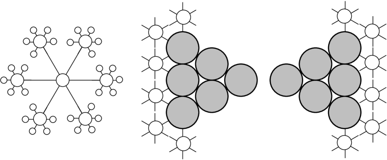
The advantage of choosing a BL over other models resides on the one hand in the lack of long-range order which mimics the poly-crystallinity of real electrodes. On the other hand the BL captures the short-range order since the local coordination of an atom is that of an atom in the bulk crystal of the corresponding material.
 |
 |
 |
The right hand side of Figure 2 illustrates schematically how the device (represented here by a single-element nanocontact) is connected to the BL electrodes: For a given chosen atom, typically in the outer planes of the device, a branch of the BL is added in the direction of any missing bulk atom (including those missing in the same plane). The directions in which tree branches are added are indicated by white small circles which represent the first atoms of the branch in that direction. This corresponds to adding a BL self-energy to the atom in that direction (see App. C for a derivation of this formula):
| (12) |
where is the sum over all self-energies in all directions and the bar in indicates the opposite direction of , i.e. . The electrode self-energies and are thus obtained by summing up the directional BL self-energies in all directions missing on that particular atom for all the atoms connected to that electrode:
| (13) |
Assuming that the most important structural details of the electrode are already included in the central cluster, the BLs should have no other relevance than that of introducing a generic bulk electrode for a given metal.
In order to compare the results of the BL model with the actual electronic structure of the corresponding real crystal lattice, we calculate the bulk DOS of the BL from the imaginary part of the local GF:
| (14) |
where the local Green’s function of the Bethe lattice is given by
| (15) |
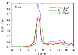
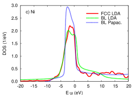
In Fig. 3 we compare the bulk DOS of BL models using different parametrizations with electronic structure calculations in the local density approximation (LDA) for the three different electrode materials considered here (Cu, Al and Ni). The BLs have coordination 12, corresponding to the FCC crystalline structure of the bulk materials. On the one hand we have taken the TB parameters directly from the nearest-neighbor hoppings and on-site energies of the LDA Kohn-Sham Hamiltonian of the FCC crystal (ignoring the overlap). where the calculations have been carried out with the help of the CRYSTAL code. On the other hand we have taken the TB parameters established by Papaconstantopoulus and coworkersMehl and Papaconstantopoulos . As can also be seen from Fig. 3, the BL construction results in all cases in a smooth DOS which reproduces the basic features of the one corresponding to a mono-crystalline solid. As can be seen in Fig. 3, depending on the type of material, the use of one set of parameters or another can result in a more accurate description. However, the choice of parameters should not be determinant in the final conductance results as long as the device is sufficiently large.
As usual we have assumed an orthonormal basis set for the Bethe lattice. On the other hand, the basis set of the device region is typically non-orthogonal. Hence, the question arises of how to match the two different levels of modeling. A straightforward approach is to orthogonalize the device basis set, for example with the Löwdin orthogonalization scheme through the transformation . Equivalently, one can de-orthogonalize the self-energies and : .
Alternatively, one can obtain the TB parameters in a non-orthogonal basis set, and take into account the overlap between orbitals on neighbouring atoms in the calculation of the BL self-energies. In this case the Dyson equation for the calculation of the BL self-energy is trivially modified as follows:
where is the overlap matrix between orbitals on neighboring atoms in the direction .
In case of a non-orthogonal basis set one has to take into account the non-diagonal part of the GF between different sites of the BL when computing the BL DOS:
This is most easily done by extending the unit cell Hamiltonian of the BL with all nearest neighbour sites, computing the GF of the extended unit cell (X0), and then taking the partial trace for the central site of the matrix product .
| (17) |
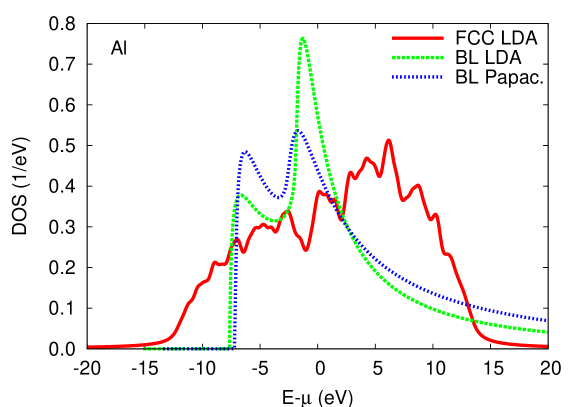
In Fig. 4 we compare the bulk DOS of BL models with different parametrizations (taking into account the overlap between orbitals on neighbouring atoms) with LDA electronic structure calculations for the case of Al. As before we have taken the TB parameters either directly from the nearest-neighbor hoppings and on-site energies of the LDA Kohn-Sham Hamiltonian of the FCC crystal (this time taking into account the overlap) or we have taken the TB parameters established by Papaconstantopoulus and coworkers (this time with overlap). Now the BL DOS does not resemble the DOS of a real crystal lattice anymore: The band width now becomes semi-infinite extending infinitely to positive energies. This artifact can only be healed by scaling down the overlap considerably. We therefore conclude that the introduction of non-orthogonal basis sets in the description of the BL does not seem to be very useful for mimicking the DOS of real materials, being preferable the self-energy deorthogonalization procedure described above.
III.2 Nanowire electrodes

The second type of model for the leads consists of finite-section wires where the electronic structure is described at the same computational level as that of the device. As indicated in Fig. 5, we subdivide the one-dimensional leads into unit cells which must be chosen sufficiently large so that the coupling between non-neighboring unit cells can be neglected. In general a unit cell consists of several primitive unit cells of the crystal. The Hamiltonian matrix of the left lead can be subdivided into sub-matrices in the following manner:
| (22) |
Analogously the Hamiltonian of the right lead is given by the following matrix:
| (23) |
In a similar way, the overlap inside the leads is given by the matrices
| (24) |
and
| (25) |
Furthermore, the unit cell of each lead that is immediately connected to the scattering region (unit cell “” for the left and unit cell “” for the right lead) is included into the device part of the system. So the Hamiltonian of the device region reads
| (26) |
and the overlap matrix is given by:
| (27) |
Since only the - and -parts of the device region are immediately connected to the two semi-infinite nanowire electrodes the self-energy matrices and that describe the coupling of the device region to the electrodes L and R are given by matrices that are different from zero only in the - and -parts, respectively:
| (31) |
and
| (35) |
As shown in App. D, the non-zero submatrices and can be calculated from the Hamiltonian and overlap sub-matrices of the two leads by the following Dyson equations:
| (36) | |||||
| (37) | |||||
IV Self-consistent electronic structure of the device
In the context of standard DFT electronic structure calculations of finite or periodic systems the self-consistent mean-field electronic potential and the density matrix (or Kohn-Sham wave functions) are determined by the sole input of the atomic structure of the cluster or cell, through the chosen exchange-correlation functional. In the context of quantum transport, where the systems are infinite, but present no translational invariance, the “boundary conditions” imposed by the electrodes play an additional and important role. The electronic structure of the device region also depends on the model chosen to represent the electrodes and the details of how to carry out the self-consistency may vary, particularly when out of equilibrium. We discuss now two different alternatives: The embedded cluster approach, associated to the use of BLs (see Sec. III.1), and the supercell approach, where the electrodes are described by nanowires (see Sec. III.2).
IV.1 Embedded cluster approach
In the embedded cluster approach the electronic structure of the infinite system is calculated self-consistently only within a finite-size region –the scattering or device region containing the nanoconstriction or molecule– while the electronic structure of the rest of the system (i.e., the two bulk electrodes) is fixed from the very beginning to that of a simplified parametrized BL model (see Sec. III.1). The basic premise here is to set up a device region sufficiently large. In other words, a sufficiently wide section of the bulk electrodes must be included in the device region so that the interface resistance between the BL and the device, the former being described at a lowest level of approximation than the latter, does not contribute significantly to the overall resistance which is essentially determined by the intrinsic resistance of the device.
In equilibrium the two leads or electrodes must have the same electrochemical potential. If the leads are made of different materials with different work functions, an overall charge transfer must occur somewhere. This gives rise to an electric field, shifting the band structures of the two leads relative to each other, and subsequently aligning the electrochemical potentials of the two leads. The net effect of the charge transfer on the electronic structure of the bulk electrode material outside the device can be taken into account by simply shifting the electrochemical potentials (and of course the band structure) of the two materials to a common electrochemical potential. Leads of the same material but presenting different crystallographic orientations might also present different work functions, but the BL model cannot account for this difference. Notice that we have refrained from being too specific about where the charge transfer takes place. A localized charge transfer in the device region, typically a one- or quasi-one-dimensional system, cannot be entirely responsible for the electrochemical alignment far away from the device for obvious electrostatic reasons. One must be cautious with the extent of the region necessary for this transfer to take place. Only for infinite two-dimensional interfaces between different materials the charge accumulates strictly at the interface. In the opposite limit of one-dimensional systems in point contact, the charge transfer must extend logarithmically into the bulkLeonard and Tersoff (1999). Regardless of where the charge transfer takes place, anyway, thermodynamical equilibrium must be reached.
Taking a common electrochemical potential , the rigid electrostatic shifts are and where and are the electrochemical potentials (or work functions) of the materials of the left and right electrode, respectively. The lead Hamiltonians corrected by the electrostatic shift are thus given by and . Now the Kohn-Sham Hamiltonian of the entire system (leads+device) is given by
| (42) | |||||
where we have included the electrochemical potential of the entire system. The corresponding overlap matrix that takes into account the non-orthogonality of the atomic orbitals has of course the same form as in eq. 2.
The Kohn-Sham Hamiltonian of the entire system depends only on the electron density of the device region since the electronic structure of the rest of the system is kept fixed (apart from the electrostatic shifts and which depend on the electrochemical potential ): . The electron density can be obtained from the density matrix of the device region:foo
| (43) |
which in turn is found by integrating (most conveniently done by analytic continuation to the complex plane) the device part of the Green’s function:
| (44) |
where the device Green’s function is given by
| (45) |
Now in order to obtain the electrochemical potential of the entire system, one has to impose charge neutrality in the entire system. Since the metallic leads outside the device region are charge neutral themselves, it suffices to impose charge neutrality within the device region:
| (46) | |||||
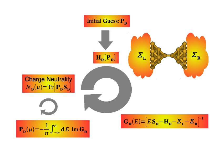
Since via is a functional of the electron density , the electronic structure of the device region can now be determined self-consistently, already having taken into consideration the effect of the leads through the selfenergies in Eq. 45. For a practical implementation of this procedure we have created an interface to the quantum chemistry code Gaussian03, taking thus advantage of the various DFT implementations that can be found in such a code. Figure 6 shows a schematic picture of the self-consistent calculation of the electronic structure of the device region as described above.
Out of equilibrium, i.e., for a finite bias one has to use the NEGF technique. In this case there is an additional contribution to the density matrix which can be calculated by integrating the so-called lesser GF within the bias window:
| (47) |
where we have assumed a positive difference between L and R electrochemical potentials, . As for the equilibrium case, charge neutrality must be imposed, e.g., by setting to the appropriate value. The lesser GF can be easily calculated from the retarded and advanced GFs:
| (48) | |||||
For a full discussion of the actual implementation of these expressions see Ref. Louis et al. (2003). We stress here we are taking into account the electron-electron interactions in the device region by an effective mean-field description at the level of DFT. Thus the device Hamiltonian is an effective Kohn-Sham one-body Hamiltonian. In this approximation to the true many-body problem Eqs. 7 and 8 remain valid even out of equilibrium and at finite temperature.
IV.2 Supercell approach
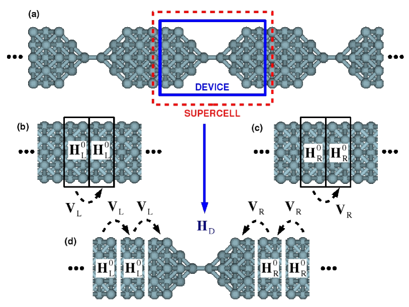
In the supercell approach we calculate the electronic structure of the device region and the electrodes with ab initio electronic structure programs for periodic systems that use localized basis sets such as Crsytal or Siesta. We first define a one-dimensional periodic system consisting of the device region as the unit cell, as shown in Fig. 7(a). It is crucial that the device part D contains a sufficiently large portion of the nanowire electrodes so as to guarantee that the electronic structure of the device region and thus the Hamiltonian is the same as the electronic structure of the device between two semi-infinite nanowires. In other words, we seek to connect the two leads L and R far enough away from the scattering region where the electronic structure has relaxed to that of a bulk (i.e., infinite) nanowire.
In a similar way, the unit cell Hamiltonian matrix and hopping matrices between unit cells for left and right leads are extracted from periodic calculations of infinite nanowires of finite width [see Fig. 7(b,c)]. The lead self-energies , which describe the coupling of the device region D to the semi-infinite nanowires L and R in the situation depicted in Fig. 7(d) can now be calculated by the Dyson equations (36) and (37).
Since the electronic structure of the electrodes has been calculated for perfect nanowires, the effect of an eventual charge transfer within the device region has not been taken into account yet. As pointed out before, the net effect of the charge transfer, mostly within the device region, on the electronic structure of the bulk electrode material outside the device can be taken into account by simply shifting the electrochemical potentials (and of course the band structure) of the two materials to a common electrochemical potential. Hence, the Kohn-Sham Hamiltonian of the entire system is also given by Eq. (42) where now the common electrochemical potential is the one obtained from the supercell calculation of the device region, and and are the electrochemical potentials obtained from the electronic structure calculations of the infinite nanowires. The Green’s function of the device region is given by eq. (45) where the self-energies and are now obtained from the Dyson equations (36) and (37) but with the energies shifted by the electrostatic shifts and :
By this procedure we have connected the device region D with two semi-infinite nanowires that have the electronic structure of bulk, i.e. infinite, nanowires far from the device.
V Comparison of electrode models
| Sequence I | Sequence II | Sequence III |
|---|---|---|
 |
 |
 |
We now compare results obtained with the two electrode models, i.e., the Bethe lattice and the nanowire electrodes and accompanying different implementations of the self-consistent procedure. We have chosen for this study an archetypal metallic nanocontact model formed by two pyramidal tips joined by the apex atoms. For the ab initio calculation of the device region and the nanowire electrodes we use LDA and the minimal valence basis set by Christian and coworkers Hurley et al. (1986). Should one be interested in a more quantitative study of the conductance of these systems it would be convenient to increase the size of the basis set, but this is not the main aim of this work. For the Bethe lattice we take the tight-binding parametrization by PapaconstantopoulosMehl and Papaconstantopoulos , obtained by fitting tight-binding parametrizations to DFT calculations. Differences between the different parametrizations discussed above are essentially irrelevant.
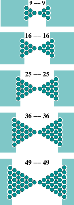
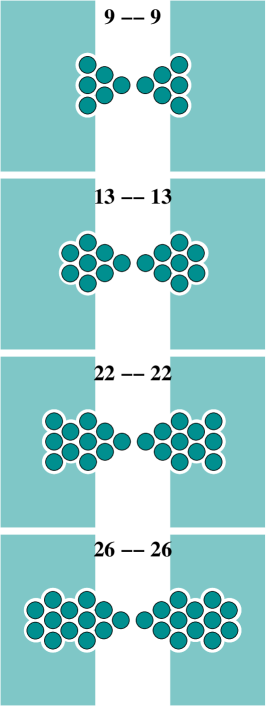
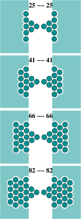
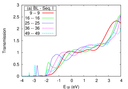
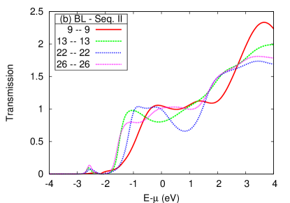
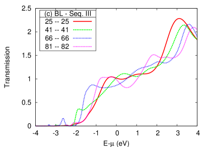
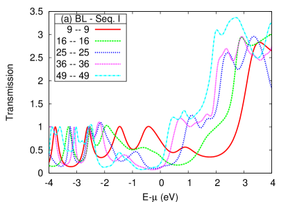
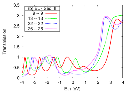
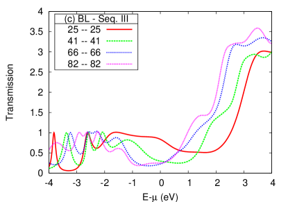
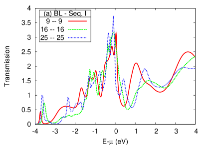
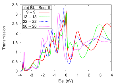
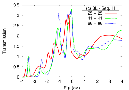
In Fig. 8 we show three different sequences of increasing size for the embedded cluster calculations with Bethe lattice electrodes. The narrowest section or contact atomic structure is maintained throughout the sequence. In sequence I, the pyramidal form is maintained for the entire device while it is increased in size. In this case the Bethe lattices are only connected to the base layers of the pyramids. In sequence II and III, only the tips maintain the pyramidal form. The rest of the device region are finite sections of 001 surfaces of the fcc crystal lattice. In each step of a sequence an atomic layer is added. The difference between sequences II and III is the width of the finite sections of bulk electrode included in the device region.
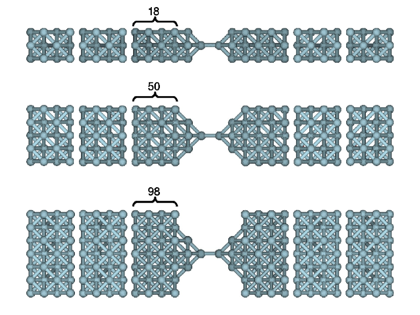
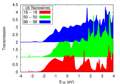
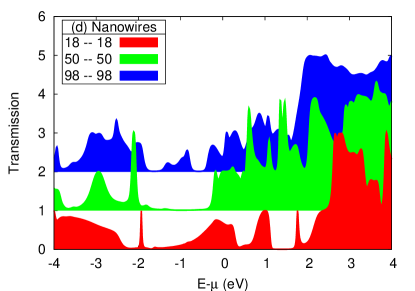
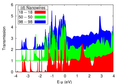
In Fig. 9 the sequence of model geometries for the case of nanowire electrodes is shown. The device region is also composed of two pyramidal tips and also contains the unit cells used for the computation of the semi infinite nanowire self-energies. In each step the section of the nanowire is increased.
V.1 An s-type conductor: Cu
 |
 |
 |
 |
First we have studied the relatively simple situation of an -type material, i.e., only -type electrons are contributing to the DOS near the Fermi level and hence to the zero-bias conductance. Here we consider Cu which is a low-resistivity metal frequently used in nano-electronics and STM experiments. Figs. 10(a)-(c) show the transmission functions (near the Fermi level) calculated with Bethe lattice electrodes. The nanocontacts share the same basic contact geometry but have different amounts of bulk electrode material included in the device region according to the different geometry sequences explained above and illustrated in Fig. 8. As can be seen the individual transmission functions vary for different geometries within each sequence and also between sequences. However, the overall shapes of the individual transmission functions are very similar. Near the Fermi level all transmission functions feature a plateau around one implying a zero-bias conductance of approximately 1 . The origin of this “quantized” conductance lies in the single open channel composed of Cu -orbitals which is almost perfectly conducting. The number and orbital composition of the conducting channels can be done as explained in Ref. Jacob and Palacios, 2006.
Fig. 10(d) shows the transmission functions for Cu nanocontacts with the same basic contact geometry as before but now with Cu nanowires of finite section serving as bulk electrodes instead of the Bethe lattices. Now the transmission functions are much spikier than before, especially at higher energies. This is somewhat reduced by increasing the width of the nanowire electrodes since the density of peaks increases and begin to merge. The origin of this fine structure in the transmission function lies in the well-defined conducting channels in the electrodesKe et al. (2005a). Interestingly, the plateau of transmission one near the Fermi level is clearly visible. Also the overall transmission curves are roughly similar to the ones obtained before with the Bethe lattice electrodes, at least for the bigger nanowires. The computational effort is, however, greatly increased in the latter case.
The relative stability of the plateau near the Fermi level with respect to changes in the size and specific form of the device region or with respect to the electrode model is of course due to the low sensitivity to elastic scattering of the very delocalized -type conduction electrons. The variations of the transmission curves for the different electrode models and device regions can still be attributed to the different interference patterns of the conduction electrons. These results are consistent with experimental evidence which shows a sharp but nevertheless finite-width peak in the conductance histogram of Cu nanocontacts at 1 .
V.2 An sp-type conductor: Al
We now turn to a slightly more complicated situation of nanocontacts made from Al which is an -type conductor. In this case we expect that changes in the geometry of the nanoconctact should have a bigger effect on the transmission than in the case of a simple -type conductor since -orbitals contributing now to the conductance are more susceptible to elastic scattering than -orbitals due to their directionality. In fact, this can be appreciated in the different sequences (see Fig. 11). Now, as the device region increases, the transmission curves present larger variability. Furthermore, the conductance at the Fermi level changes noticeably, approaching a definite value only for large systems where we consistently obtain zero-bias conductances below 0.5 . This result does not seem to be in agreement with experimental evidence showing, typically, zero-bias conductances between 0.5 and 1 for the last conductance plateau before breakingYanson and Ruitenbeek (1995). We remind the reader, however, that a much more complete statistical analysis is needed to draw conclusions in this regard. This analysis was carried out in the pastHasmy et al. (2005) and a good agreement was found between theory and the experimental results. A common feature to most transmission curves is a pronounced increase above the Fermi level. This shoulder or peak originates from the doubly-degenerate ,-channel while the transmission through the - and -channels is suppressedCuevas et al. (1998). Again the transmission functions obtained with the finite-section nanowire electrodes present more structure [see Fig. 11(d)], eventually converging to the overall shape obtained with the Bethe lattice electrodes for large enough section electrodes.
 |
 |
 |
 |
V.3 An sd-type conductor: Ni
As a last example we consider the case of a nanocontact made out of Ni, an material. This case is the more complex from the point of view of the electronic structure since, in principle, 6 orbitals are expected to contribute to the conductance at the Fermi level. For simplicity’s sake, we consider paramagnetic Ni, where the two spin channels contribute equally to the current. A realistic theoretical treatment aiming at understanding the available experimental results of truely magnetic Ni has been presented in the pastJacob et al. (2005); Calvo et al. (2008) and will not be repeated here. Contrary to what one might expect, the transmission at the Fermi level does not depend too much on the chosen size of the central region or device when using Bethe lattice electrodes, keeping a fairly constant value around 3 even for the smallest systems. It is, again, in the case of using nanowire electrodes that becomes apparent that one needs to increase the section of the wires before converging to a similar number, at the concommitant computational cost. The orbital analysis indicates that the -channel and two -channels are mainly the ones responsible for this number. Away from the Fermi level the variations among curves are similar to the ones in the previous cases, hardly exceeding in magnitude the transmission unity.
 |
 |
 |
 |
VI Discussion and Conclusions
We have presented a detailed account of the theoretical and computational treatment of quantum transport in nanostructures. While similar analysis have been reported in the past, ours mainly focuses on implementation details usually skipped in the literature, but crucial for those interested in developing codes as the two presented here. In addition to the well-known pitfalls in the use of DFT in transport problems, the way this implementation is carried out determines, to a good extent, the results or the difficulty in obtaining reliable results that can be compared with experiments. We have thus made a critical comparison between to archetypal types of electrodes, which is a source of discrepancy and controversy: parametrized vs. ab initio. Without pretending our two codes to be representative of all the other developed by many groups, we can conclude that the use of parametrized electrodes presents two advantages with respect to a more faithful description of the electronic structure of the electrodes. First, the variability between transmission curves is greatly reduced even for small devices or central regions when compared to the use of nanowire electrodes. Second, the computational cost in the calculation of the self-energy in the former case can be orders of magnitude smaller than in the latter, particularly for large section wires. The use of semiinfinite wires as electrodes is, nevertheless, essential to properly understand scattering in a variety of systems such as true semiconducting nanowires, atomic chainsJacob et al. (2008), carbon nanotubes, or graphene nanoribbonsMunoz-Rojas et al. (2006).
Acknowledgements
This work has been partially funded by Spanish MICINN under Grants Nos. FIS2010-21883-C02-02 and CONSOLIDER CSD2007-00010.
Appendix A Representation of operators in non-orthogonal basis sets
The natural definition for the matrix of a one-body operator in a non-orthogonal basis set (NOBS) is simply by its matrix elements:
| (51) |
However, the representation of an operator in a NOBS is not that simple:
| (52) |
where is the overlap matrix. It is easy to see that this definition leads results in the matrix elements defined above. Then the identity operator in the NOBS representation is given by
| (53) |
which is also easy to proof.
Now we define a second matrix
| (54) |
which is the matrix that appears above in the representation of the operator in a NOBS.
One should take care when using the representation of an operator in a NOBS. For example, the matrix element of an operator between two non-orthogonal orbitals can be zero, , but the corresponding matrix element of the matrix does not necessarily vanish due to the multiplication with the inverse of the overlap matrix on both sides. Thus there is actually a non-zero contribution of the two orbitals to the operator although the corresponding matrix element of the operator is zero
Orthogonalizing the basis set by the Löwdin orthogonalization scheme Szabo and Ostlund (1989), the matrices and are transformed to the matrix defined in the new orthogonal basis set according to:
| (55) |
Though there are also other orthogonalization schemes, the Löwdin scheme is particularly useful in the context of quantum chemistry methods based on atomic orbitals as the center of the orthogonalized orbital remains centered on the same atom as the original non-orthogonal orbital.
Appendix B Partitioning method
As explained in Sec. II we model the transport problem by dividing the system in three parts. Two semi-infinite leads (L) and (R) with bulk electronic structure are connected to a finite region called device (D). In a local basis set the Hamiltonian and the overlap matrix of the system are given by (1) and (2). Dividing the F matrix into sub-matrices in a similar manner we obtain the following matrix equation:
This yields 9 equations for the 9 sub-matrices of the GF . We can resolve this matrix equation columnwise. Multiplying all rows of with the first column of yields three equations for , and which yield:
Similarly we obtain from multiplication with the second column:
And finally from multiplication with the third column, we obtain:
We have introduced the Green’s functions of the isolated left and right lead and and the corresponding self-energies and :
Furthermore, we have defined the Green’s function of the device plus the left lead only, , of the device plus the right lead only, , and the corresponding self-energies and each one representing the coupling of one of the leads to the device and the other lead:
Appendix C Bethe lattices
In this appendix we discuss how self-energies for Bethe lattices (BL) used to describe the leads are calculated. A BL is generated by connecting a site with nearest-neighbors in directions that could be those of a particular crystalline lattice. The new sites are each one connected to different sites and so on and so forth. The generated lattice has the actual local topology (number of neighbors and crystal directions) but has no rings, and thus does not describe the long range order characteristic of real crystals. Let be a generic site connected to one preceding neighbor and neighbors of the following shell ( with ). For simplicity’s sake, we carry out the derivation for an orthogonal basis. Following App. D. the generalization to the case of a non-orthogonal basis is straigthforward.
Dyson’s equation for an arbitrary non-diagonal Green’s function is
| (58) |
where is an arbitrary site, the energy, and is a matrix that incorporates interactions between orbitals at sites and (bold capital characters are used to denote matrices). is a diagonal matrix containing the orbital levels and is the identity matrix. Then, we define a transfer matrix as
| (59) |
Multiplying Eq. (58) by the inverse of we obtain,
| (60) |
Due to the absence of rings the above equation is valid for any set of lattice sites, and, thus, solving the BL is reduced to a calculation of a few transfer matrices. Note that a transfer matrix such as that of Eq. (59) could also be defined in a crystalline lattice but, in that case it would be useless.
Eq. (60) can be solved iteratively,
| (61) |
If the orbital basis set and the lattice have full symmetry (including inversion symmetry) the different transfer matrices can be obtained from just a single one through appropriate rotations. However this is not always the case (see below).
Before proceeding any further we define self-energies that can be (and commonly are) used in place of transfer matrices,
| (62) |
Eq. (61) is then rewritten as,
| (63) |
where we have made use of the general property .
As discussed hereafter, in a general case of no symmetry this would be a set of coupled equations ( if there is no inversion symmetry). Symmetry can be broken due to either the spatial atomic arrangement, the orbitals on the atoms that occupy each lattice site, or both. When no symmetry exists, the following procedure has to be followed to obtain the self-energy in an arbitrary direction. The method is valid for any basis set or lattice. Let be the nearest-neighbor directions of the lattice we are interested in and the interatomic interaction matrix in these directions. To make connection with the notation used above note that the vector that joins site to site , namely, would necessarily be one of the lattice directions of the set . The self-energies associated to each direction have to be obtained from the following set of coupled self-consistent equations,
| (64) |
| (65) |
where and . is the interatomic interaction in the direction, and and are the sums of the self-energy matrices entering through all the Cayley tree branches attached to an atom and their inverses, respectively, i.e.
| (66) |
This set of matrix equations has to be solved iteratively. It is straightforward to check that, in cases of full symmetry, it reduces to the single equation. The local density of states can be obtained from the diagonal Green’s function matrix,
| (67) |
Appendix D Self-energy of a one-dimensional lead
Here we will derive the Dyson equation (37) for the calculation of the self-energy of the semi-infinite right lead. The derivation of the Dyson equation for the left lead (36) goes in a completely analogous way.
The Hamiltonian matrix of the (isolated) semi-infinite right electrode is defined in eq. (23) as:
| (68) |
and the overlap matrix is given in eq. (25) as:
| (69) |
To obtain the self-energy of the lead we have to calculate the GF of the lead from its defining equation:
| (70) |
In the same way as the Hamiltonian and the overlap matrix we subdivide the GF matrix into sub-matrices corresponding to the unit cells of the lead. Now the above equation for the right lead’s GF reads:
| (80) |
As explained in Sec.III.2 it suffices to calculate the “surface” GF, i.e. . From multiplication of the 1st, the 2nd and so on until the -th line of with the 1st column of we get the following chain of equations:
| (82) | |||||
| (84) |
For the equations for determining all have the same structure:
| (85) |
We define a transfer matrix for by:
| (86) |
The transfer matrix thus transfers information from site to site of the lead, i.e. from the left to the right. Multiplying Eq. (85) by we obtain:
Reordering we obtain the following iterative equation for the transfer matrices:
Since the electrode is semi-infinite it looks the same from each unit cell when looking to the right. Thus a given , results always in the same independent of . Thus the transfer matrix must be independent of : , and Eq. (D) allows to determine the self-consistently.
We define the self-energy as , and obtain the Dyson equation for the self-energy:
We will now see that this self-energy is indeed identical to the one defined for the right lead in eq. (37), i.e. . By plugging in the definition of the transfer matrix, eq. (86), into eq. (82) for determining the surface GF, we find:
Plugging in the definition of the self-energy we obtain:
| (90) |
Thus we obtain for the surface GF of the right lead:
| (91) |
And vice-versa the self-energy can be expressed in terms of the surface GF:
| (92) |
This proofs that the self-energy defined above in terms of the transfer matrix is identical to the self-energy defined earlier in Sec.III.2 so that the self-energy can be calculated iteratively by the Dyson equation (37).
The proof for the left lead runs completely analogously. The surface GF of the left lead is now:
| (93) |
References
- Agraït et al. (2003) N. Agraït, A. L. Yeyati, and J. M. v. Ruitenbeek, Physics Reports 377, 81 (2003), and references therein.
- Lang (1995) N. D. Lang, Phys. Rev. B 52, 5335 (1995).
- Di Ventra et al. (2000) M. Di Ventra, S. T. Pantelides, and N. D. Lang, Phys. Rev. Lett. 84, 979 (2000).
- Taylor et al. (2001) J. Taylor, H. Guo, and J. Wang, Phys. Rev. B 63, 121104 (2001).
- Palacios et al. (2001) J. J. Palacios, A. J. Pérez-Jiménez, E. Louis, and J. A. Vergés, Phys. Rev. B 64, 115411 (2001).
- Xue et al. (2001) Y. Xue, S. Datta, and M. A. Ratner, J. Chem. Phys. 115, 4292 (2001).
- Palacios et al. (2002) J. J. Palacios, A. J. Pérez-Jiménez, E. Louis, E. SanFabián, and J. A. Vergés, Phys. Rev. B 66, 035322 (2002).
- Brandbyge et al. (2002) M. Brandbyge, J. L. Mozos, P. Ordejón, J. Taylor, and K. Stokbro, Phys. Rev. B 65, 165401 (2002).
- Heurich et al. (2002) J. Heurich, J. C. Cuevas, W. Wenzel, and G. Schön, Phys. Rev. Lett. 88, 256803 (2002).
- Ventra and Lang (2002) M. D. Ventra and N. D. Lang, Phys. Rev. B 65, 045402 (2002).
- Palacios et al. (2003) J. J. Palacios, A. J. Pérez-Jiménez, E. Louis, E. SanFabián, and J. A. Vergés, Phys. Rev. Lett. 90, 106801 (2003).
- Fujimoto and Hirose (2003) Y. Fujimoto and K. Hirose, Phys. Rev. B 67, 195315 (2003).
- Louis et al. (2003) E. Louis, J. A. Vergés, J. J. Palacios, A. J. Pérez-Jiménez, and E. SanFabián, Phys. Rev. B 67, 155321 (2003).
- Xue and Ratner (2003a) Y. Xue and M. A. Ratner, Phys. Rev. B 68, 115406 (2003a).
- Xue and Ratner (2003b) Y. Xue and M. A. Ratner, Phys. Rev. B 68, 115407 (2003b).
- Basch and Ratner (2003) H. Basch and M. A. Ratner, J. Chem. Phys. 119, 11926 (2003).
- Jelínek et al. (2003) P. Jelínek, R. Pérez, J. Ortega, and F. Flores, Phys. Rev. B 68, 085403 (2003).
- Ke et al. (2004) S.-H. Ke, H. U. Baranger, and W. Yang, Phys. Rev. B 70, 085410 (2004).
- Hirose et al. (2004) K. Hirose, N. Kobayashi, and M. Tsukada, Phys. Rev. B 69, 245412 (2004).
- Xue and Ratner (2004) Y. Xue and M. A. Ratner, Phys. Rev. B 70, 081404 (2004).
- Liang et al. (2004) G. C. Liang, A. W. Ghosh, M. Paulsson, and S. Datta, Phys. Rev. B 69, 115302 (2004).
- Rocha and Sanvito (2004) A. R. Rocha and S. Sanvito, Phys. Rev. B 70, 094406 (2004).
- Frederiksen et al. (2004) T. Frederiksen, M. Brandbyge, N. Lorente, and A. P. Jauho, Phys. Rev. Lett. 93, 256601 (2004).
- Thygesen and Jacobsen (2005) K. S. Thygesen and K. W. Jacobsen, Phys. Rev. B 72, 033401 (2005).
- Evers et al. (2004) F. Evers, F. Weigend, and M. Koentopp, Phys. Rev. B 69, 235411 (2004).
- Tada et al. (2004) T. Tada, M. Kondo, and K. Yoshizawa, J. Chem. Phys. 121, 8050 (2004).
- Nara et al. (2004) J. Nara, W. T. Geng, H. Kino, N. Kobayashi, and T. Ohno, J. Chem. Phys. 121, 6485 (2004).
- Ferretti et al. (2005) A. Ferretti, A. Calzolari, R. D. Felice, F. Manghi, M. J. Caldas, M. B. Nardelli, and E. Molinari, Phys. Rev. Lett. 94, 116802 (2005).
- Toher et al. (2005) C. Toher, A. Filippetti, S. Sanvito, and K. Burke, Phys. Rev. Lett. 95, 146402 (2005).
- Fujimoto et al. (2005) Y. Fujimoto, Y. Asari, H. Kondo, J. Nara, and T. Ohno, Phys. Rev. B 72, 113407 (2005).
- Asari et al. (2005) Y. Asari, J. Nara, N. Kobayashi, and T. Ohno, Phys. Rev. B 72, 035459 (2005).
- Wu et al. (2005) X. Wu, Q. Li, J. Huang, and J. Yang, J. Chem. Phys. 123, 184712 (2005).
- Choi et al. (2005) Y. C. Choi, W. Y. Kim, K. S. Park, P. Tarakeshwar, K. S. Kim, T. S. Kim, and J. Y. Lee, J. Chem. Phys. 122, 094706 (2005).
- Ke et al. (2005a) S. H. Ke, H. U. Baranger, and W. T. Yang, J. Chem. Phys. 123, 114701 (2005a).
- Ke et al. (2005b) S. H. Ke, H. U. Baranger, and W. T. Yang, J. Chem. Phys. 122, 074704 (2005b).
- Bagrets et al. (2006) A. Bagrets, N. Papanikolaou, and I. Mertig, Phys. Rev. B 73, 045428 (2006).
- Smogunov et al. (2006) A. Smogunov, A. DalCorso, and E. Tosatti, Phys. Rev. B 73, 075418 (2006).
- Jiang et al. (2006) J. Jiang, M. Kula, and Y. Luo, J. Chem. Phys. 124, 034708 (2006).
- Havu et al. (2006) P. Havu, V. Havu, M. J. Puska, M. H. Hakala, A. S. Foster, and R. M. Nieminen, J. Chem. Phys. 124, 054707 (2006).
- Hod et al. (2006) O. Hod, J. E. Peralta, and G. E. Scuseria, J. Chem. Phys. 125, 114704 (2006).
- Rocha et al. (2006) A. R. Rocha, V. M. Garcia-Suarez, S. Bailey, C. Lambert, J. Ferrer, and S. Sanvito, Phys. Rev. B 73, 085414 (2006).
- Nakamura and Yamashita (2006) H. Nakamura and K. Yamashita, J. Chem. Phys. 125, 194106 (2006).
- Prociuk et al. (2006) A. Prociuk, B. Van Kuiken, and B. D. Dunietz, J. Chem. Phys. 125, 204717 (2006).
- Mera et al. (2007) H. Mera, P. Bokes, and R. W. Godby, Phys. Rev. B 76, 125319 (2007).
- Mizuseki et al. (2007) H. Mizuseki, R. V. Belosludov, T. Uehara, S. U. Lee, and Y. Kawazoe, in 4th Conference of the Asian-Consortium-on-Computational-Materials-Science (Seoul, South Korea, 2007), pp. 1197–1201.
- Nakamura (2007) H. Nakamura, in 12th International Conference on Vibrations at Surfaces (Erice, Italy, 2007).
- Qian et al. (2007) Z. Qian, R. Li, S. Hou, Z. Xue, and S. Sanvito, J. Chem. Phys. 127, 194710 (2007).
- Thygesen and Rubio (2007) K. S. Thygesen and A. Rubio, J. Chem. Phys. 126, 091101 (2007).
- Pauly et al. (2008) F. Pauly, J. K. Viljas, U. Huniar, M. Hafner, S. Wohlthat, M. Burkle, J. C. Cuevas, and G. Schon, New J. Phys. 10, 125019 (2008).
- Liu et al. (2008) H. Liu, N. Wang, J. Zhao, Y. Guo, X. Yin, F. Y. C. Boey, and H. Zhang, Chem. Phys. Chem. 9, 1416 (2008).
- Bernholc et al. (2008) J. Bernholc, M. Hodak, and W. Lu, J. Phys.: Condens. Matter 20, 294205 (2008).
- Li et al. (2008a) Y. Li, G. Yin, J. Yao, and J. Zhao, Comput. Mater. Sci. 42, 638 (2008a).
- Oetzel et al. (2008) B. Oetzel, M. Preuss, F. Ortmann, K. Hannewald, and F. Bechstedt, Phys. Stat. Sol. B 245, 854 (2008).
- Jelinek et al. (2008) P. Jelinek, R. Perez, J. Ortega, and F. Flores, Phys. Rev. B 77, 115447 (2008).
- Bredow et al. (2008) T. Bredow, C. Tegenkamp, H. Pfnur, J. Meyer, V. V. Maslyuk, and I. Mertig, J. Chem. Phys. 128, 064704 (2008).
- Hyldgaard (2008) P. Hyldgaard, Phys. Rev. B 78, 165109 (2008).
- Kondo et al. (2008) H. Kondo, J. Nara, H. Kin, and T. Ohno, Jap. J. Appl. Phys. 47, 4792 (2008).
- Li et al. (2008b) Y. W. Li, G. P. Yin, J. H. Yao, and J. W. Zhao, Comput. Mater. Sci. 42, 638 (2008b).
- Mowbray et al. (2008) D. J. Mowbray, G. Jones, and K. S. Thygesen, J. Chem. Phys. 128, 111103 (2008).
- Smeu et al. (2008) M. Smeu, R. A. Wolkow, and G. A. DiLabio, J. Chem. Phys. 129, 034707 (2008).
- Thygesen (2008) K. S. Thygesen, Phys. Rev. Lett. 100 (2008).
- Yoshizawa et al. (2008) K. Yoshizawa, T. Tada, and A. Staykov, Journal of the American Chemical Society 130, 9406 (2008).
- Zhao and Dunietz (2008) Z. Zhao and B. D. Dunietz, J. Chem. Phys. 129, 024702 (2008).
- Garcia-Lekue and Wang (2009) A. Garcia-Lekue and L. W. Wang, Comput. Mater. Sci. 45, 1016 (2009).
- Gutierrez et al. (2009) R. Gutierrez, R. A. Caetano, B. P. Woiczikowski, T. Kubar, M. Elstner, and G. Cuniberti, Phys. Rev. Lett. 102 (2009).
- Lopez-Bezanilla et al. (2009) A. Lopez-Bezanilla, F. Triozon, S. Latil, X. Blase, and S. Roche, Nano Letters 9, 940 (2009).
- Wang and Guo (2009) J. Wang and H. Guo, Phys. Rev. B 79, 045119 (2009).
- Jacob et al. (2009) D. Jacob, K. Haule, and G. Kotliar, Phys. Rev. Lett. 103, 016803 (2009).
- Frisch et al. (2003) M. J. Frisch, G. W. Trucks, H. B. Schlegel, G. E. Scuseria, M. A. Robb, J. R. Cheeseman, J. A. Montgomery, J. , T. Vreven, K. N. Kudin, et al., GAUSSIAN03, Revision B.01, Gaussian, Inc., Pittsburgh PA, 2003 (2003).
- Dovesi et al. (2006) R. Dovesi, V. R. Saunders, C. Roetti, R. Orlando, C. M. Zicovich-Wilson, F. Pascale, B. Civalleri, K. Doll, N. M. Harrison, I. J. Bush, et al., CRYSTAL06, Release 1.0.2, Theoretical Chemistry Group - Universita’ Di Torino - Torino (Italy) (2006).
- Ordejón et al. (1996) P. Ordejón, E. Artacho, and J. M. Soler, Phys. Rev. B 53, 10441 (1996).
- Trouwborst et al. (2008) M. L. Trouwborst, E. H. Huisman, F. L. Bakker, S. J. van der Molen, and B. J. van Wees, Phys. Rev. Lett. 100, 175502 (2008).
- (73) J. J. Palacios, D. Jacob, A. J. Pérez-Jiménez, E. S. Fabián, E. Louis, and J. A. Vergés, ALACANT ab-initio quantum transport package, URL http://alacant.dfa.ua.es.
- Economou (1970) E. N. Economou, Green’s functions in Quantum Physics, no. 7 in Springer Series in Solid State Physics (Springer, Berlin-Heidelberg-New York-Tokyo, 1970).
- Landauer (1970) R. Landauer, Philos. Mag. 21, 863 (1970).
- Caroli et al. (1971) C. Caroli, R. Combescot, and P. Dederichs, J. Phys. C: Sol. State Phys. 4, 916 (1971).
- Burke et al. (2006) K. Burke, M. Koentopp, and F. Evers, Phys. Rev. B 73, 121403 (2006).
- (78) M. J. Mehl and D. A. Papaconstantopoulos, URL http://cst-www.nrl.navy.mil/bind/.
- Leonard and Tersoff (1999) F. Leonard and J. Tersoff, Phys. Rev. Lett. 83, 5174 (1999).
- (80) In the case of a non-orthogonal basis set there is actually an ambiguity in the exact definition of the electronic charge of a subspace and hence also in the definition of the corresponding electron density.
- Hurley et al. (1986) M. M. Hurley, L. F. Pacios, P. A. Christiansen, R. B. Ross, and W. C. Ermler, J. Chem. Phys 84, 6840 (1986).
- Jacob and Palacios (2006) D. Jacob and J. J. Palacios, Phys. Rev. B 73, 075429 (2006).
- Yanson and Ruitenbeek (1995) A. I. Yanson and J. M. Ruitenbeek, Phys. Rev. Lett. 79, 2157 (1995).
- Hasmy et al. (2005) A. Hasmy, A. J. Pérez-Jiménez, J. J. Palacios, P. García-Mochales, J. L. Costa-Krämer, M. Díaz, E. Medina, and P. A. Serena, Phys. Rev. B 72, 245405 (2005).
- Cuevas et al. (1998) J. C. Cuevas, A. Levy Yeyati, A. Martín-Rodero, G. Rubio Bollinger, C. Untiedt, and N. Agraït, Phys. Rev. Lett. 81, 2990 (1998).
- Jacob et al. (2005) D. Jacob, J. Fernández-Rossier, and J. J. Palacios, Phys. Rev. B 71, 220403 (2005).
- Calvo et al. (2008) M. R. Calvo, M. J. Caturla, D. Jacob, C. Untiedt, and J. J. Palacios, IEEE Transactions in Nanotechnology 7, 165 (2008).
- Jacob et al. (2008) D. Jacob, J. Fernandez-Rossier, and J. J. Palacios, Phys. Rev. B 77, 165412 (2008).
- Munoz-Rojas et al. (2006) F. Munoz-Rojas, D. Jacob, J. Fernandez-Rossier, and J. J. Palacios, Phys. Rev. B 74, 195417 (2006).
- Szabo and Ostlund (1989) A. Szabo and N. S. Ostlund, Modern Quantum Chemistry (McGraw-Hill, New York, 1989).