Deterministic nano-assembly of a coupled quantum emitter - photonic crystal cavity system
Abstract
Controlling the interaction of a single quantum emitter with its environment is a key challenge in quantum optics. Here, we demonstrate deterministic coupling of single Nitrogen-vacancy (NV) centers to high-quality photonic crystal cavities. We pre-select single NV centers and position their 50 nm-sized host nanocrystals into the mode maximum of photonic crystal S1 cavities with few-nanometer accuracy. The coupling results in a strong enhancement of NV center emission at the cavity wavelength.
Spontaneous light emission can be controlled by enhancing or suppressing the vacuum fluctuations of the electromagnetic field at the location of the light source Mandel . When placed into highly confined optical fields, such as those created in optical cavities or plasmonic structures, the optical properties of single quantum emitters can change drastically Novotny ; Noda ; Kuhn ; Schietinger . In particular, photonic crystal (PC) cavities show high quality factors combined with an extremely small mode volume Akahane . It is challenging however to efficiently couple single photon sources to a PC cavity because the emitter has to be positioned in the localized optical mode, which is confined to an extremely small volume with a size of about a wavelength Hennessy ; Rivoire ; Thon .
Nitrogen-vacancy (NV) centers in diamond are promising candidates for application as solid state quantum bits Hanson ; Neumann ; Togan . Long distance entanglement between NV centers enabling quantum repeater protocols may be achieved by two-photon quantum interference Barrett ; Childress , but is hindered by the NV centers’ weak coherent photon emission rate. Being able to control and reshape the emission spectrum of a single NV center is therefore not only of fundamental interest, but could also have potential applications in solid state quantum information processing Jiang .
Fabrication of high-quality PC cavities in diamond would be a natural way to control the emission properties of embedded NV centers, but this is challenging because of the difficulties in growing and etching diamond single-crystal thin films Greentree ; Wang . An alternative, hybrid approach is to position a diamond nanocrystal with a single NV center near a PC cavity of a different material Barth ; Englund ; Wolters ; Stewart . Because of the small size of such a crystal, the NV center can be placed in the highly confined optical mode where coupling can be efficient.
Here, we demonstrate the deterministic nano-assembly of coupled single NV center - PC cavity systems by positioning 50 nm sized diamond nanocrystals into gallium phosphide S1 cavities located on a different chip. The S1 cavity offers unique advantages over the well-studied L3 cavity Englund ; Wolters . Whereas in the L3 cavity the mode maximum is confined within the dielectric material, the mode maximum of the S1 cavity is localized in the air holes surrounding the cavity, making it accessible for coupling to external emitters. We are able to pick up and place a pre-selected diamond nanocrystal exactly into the mode maximum of a PC cavity, due to the versatility of our nanopositioning method. The coupling of a single NV center to a PC cavity is evidenced by a Purcell-enhanced spontaneous emission rate at the cavity resonance frequency.
Our samples were grown by molecular beam epitaxy on a (100) gallium phosphide (GaP) wafer, with a 1 m sacrificial layer of Al0.75Ga0.25P, and a 120 nm GaP membrane layer. Photonic crystal cavities were defined by e-beam lithography, followed by inductively coupled plasma etching to transfer the resist pattern into the substrate. An HF chemical wet etch selectively undercuts the sacrificial layer, leaving a free-standing membrane. Structure parameters were optimized using Finite-Difference-Time-Domain (FDTD) simulations. The lowest energy mode of these cavities generally has the highest quality factor, up to 3,800 for S1 cavities, to our knowledge the highest reported value for a S1 photonic crystal cavity at these wavelengths.
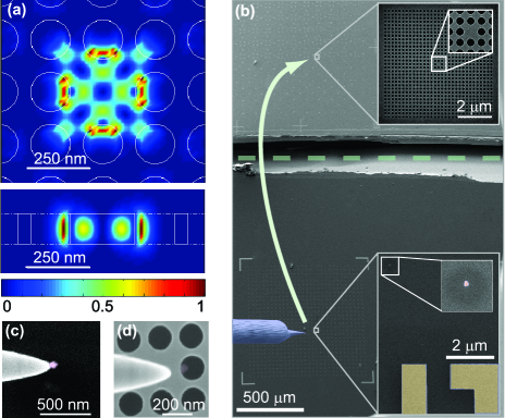
We assemble a coupled single NV center - PC cavity system by nanopositioning a diamond nanocrystal into an air hole surrounding the cavity vanderSar , where the S1 cavity has its maximum field intensity (Fig. 1a). First, a home-built confocal microscope is used to locate and identify single NV centers on a chip that contains a sparse dispersion of diamond nanocrystals. We then select NV centers that do not show switching from the negatively charged state to the neutral state Bradac . By accurately measuring the position of a candidate NV center with respect to a gold marker (fabricated using electron beam lithography), we can identify the host nanocrystal inside a scanning electron microscope (SEM) (Fig. 1b). This SEM contains a home-built nanomanipulator with a sharp tungsten tip that is mounted on a piezoelectric stage with sub-nanometer positioning accuracy Heeres . With this tip we can pick up a nanocrystal (Fig. 1c), and position it in an arbitrary new location on a different chip. Here, we position a nanocrystal that contains a single NV center into the hole of an S1 cavity (Fig. 1d) Movies .
When an NV center is successfully coupled to the cavity, it will show an enhanced spontaneous emission rate at the cavity wavelength by means of the Purcell effect Mandel . Compared to the spectrum of the NV center before positioning, the spectrum of the coupled system shows a sharp Fano-shaped resonance at the cavity frequency (Fig. 2a) Barclay ; Galli ; ZPL1 .
To verify that the spectrum originates from a single NV center we perform a second-order auto-correlation measurement on photon detection times. After correcting for background luminescence caused by substrate photoluminescence (PL), we find an antibunching dip below 0.5 (Fig. 2b) Kurtsiefer ; ZPL . The presence of a single NV center is also confirmed by the level of the observed PL. This in agreement with our previous studies vanderSar where we found that single NV centers are not affected by the nanopositioning.
To verify that the NV center is coupled to the cavity, we measure the spectrum of the NV center in the cavity (middle panel Fig. 2a) as a function of optical excitation power. By fitting this data, (inset middle panel Fig. 2a), we obtain the amplitude of the cavity resonance and the zero-phonon line (ZPL) as a function of optical excitation power (Fig. 2c). In addition to a linear component caused by background luminescence coupling to the cavity, we observe the same saturation behavior for the cavity resonance as for the NV center’s zero-phonon line. This in contrast to the purely linear increase of background luminescence measured in cavities without NV centers (data not shown). We conclude that the cavity is being fed by single photons from the NV center, as the finite optical lifetime of the NV center puts an upper limit on the photon emission rate AdditionalData .
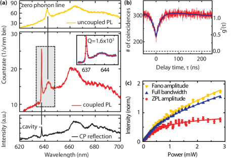
The Purcell-enhancement of the emission at the cavity wavelength can be estimated from the spectrum and the relative detection efficiencies of cavity emission and NV center emission. After subtracting the linear background contribution from the spectrum in Fig. 2a (middle panel), we find that coupling to the cavity has increased the relative intensity of detected NV emission at the cavity wavelength by a factor 4. This underestimates the actual Purcell enhancement because far-field detection of light emitted by an S1 cavity is relatively inefficient due to a large mode mismatch between the cavity and detection channel Badolato . By comparing the detection efficiency of S1 cavity emission (obtained by calculating its far-field emission profile following the method described in Vuckovic2002 ) to the detection efficiency of directly detected NV center emission, we estimate the actual Purcell enhancement to be 25. For comparison, the calculated Purcell enhancement for an optimally oriented NV center is 100. By adding efficient on-chip PC outcoupling structures or by optimizing the far-field emission profile of the cavity Tran ; Portalupi , the detection efficiency can be increased, allowing the full cavity-enhanced emission to be exploited.
In conclusion, we have demonstrated the coupling of single NV centers to S1 PC cavities by positioning 50 nm-sized diamond nanocrystals exactly into the cavity mode maximum. By pre-selecting nanocrystals with single NV centers that have rare but highly desirable optical properties such as a lifetime limited linewidth Shen , our method could be applied to reshape the NV center spectrum for a more efficient emission of coherent photons. We envision that nano-assembled, coupled NV center-cavity systems could serve as building blocks for quantum optical engineering, potentially leading to the first observation of entanglement between distant NV centers.
This work is supported by stichting voor Fundamenteel Onderzoek der Materie (FOM) and the Nederlandse Organisatie voor Wetenschappelijk Onderzoek (NWO). T.H.O. acknowledges support from Technologiestichting STW and from an ERC Starting Grant. D. B. acknowledges support from NSF grant 0901886 and Marie Curie EXT-CT-2006-042580. J. H. acknowledges support from a U. S. Department of Education GAANN grant.
References
- (1) L. Mandel, and E. Wolf, Cambridge Univ. Press, Cambridge (1995).
- (2) L. Novotny, and B. Hecht, Cambridge Univ. Press, Cambridge (2006).
- (3) S. Noda, M. Fujita, and T. Asano, Nature Photonics 1, 449-458 (2007).
- (4) S. Kühn, U. Håkanson, L. Rogobete, and V. Sandoghdar, Physical Review Letters 97, 1-4 (2006).
- (5) S. Schietinger, T. Schröder, and O. Benson, Nano Letters 8, 3911-5 (2008).
- (6) Y. Akahane, T. Asano, B.S. Song, and S. Noda, Nature 425, 944-947 (2003).
- (7) K. Hennessy, A. Badolato, M. Winger, D. Gerace, M. Atatüre, S. Gulde, S. Fält, E.L. Hu, and A. Imamoğlu, Nature 445, 896-9 (2007).
- (8) K. Rivoire, A. Kinkhabwala, F. Hatami, W. Ted Masselink, Y. Avlasevich, K. Müllen, W.E. Moerner, and J. Vučković, Applied Physics Letters 95, 123113 (2009).
- (9) S.M. Thon, M.T. Rakher, H. Kim, J. Gudat, W.T.M. Irvine, P.M. Petroff, and D. Bouwmeester, Applied Physics Letters 94, 111115 (2009).
- (10) R. Hanson, and D.D. Awschalom, Coherent manipulation of single spins in semiconductors, Nature 453, 1043-9(2008).
- (11) P. Neumann, N. Mizuochi, F. Rempp, P. Hemmer, H. Watanabe, S. Yamasaki, V. Jacques, T. Gaebel, F. Jelezko, and J. Wrachtrup, Science 320, 1326-9 (2008).
- (12) E. Togan, Y. Chu, a. S. Trifonov, L. Jiang, J. Maze, L. Childress, M. V. G. Dutt, a. S. Sörensen, P. R. Hemmer, a. S. Zibrov, and M.D. Lukin, Nature 466, 730-734 (2010).
- (13) S. Barrett, and P. Kok, Physical Review A 71, 2-5 (2005).
- (14) L. Childress, J. Taylor, A. Sørensen, and M.D. Lukin, Physical Review A 72, 1-16 (2005).
- (15) L. Jiang, J. Taylor, A. Sørensen, and M.D. Lukin, Physical Review A 76, 1-22 (2007).
- (16) A.D. Greentree, B.A. Fairchild, F.M. Hossain, and S. Prawer, Materials Today 11, 22 31 (2008).
- (17) C. F. Wang, R. Hanson, D. D. Awschalom, E. L. Hu, T. Feygelson, J. Yang, and J. E. Butler, Applied Physics Letters, 91, 201112-3, (2010)
- (18) Michael Barth, N. Nüsse, B. Löchel, and O. Benson, Optics Letters 34, 1108 1110 (2009).
- (19) D. Englund, B. Shields, K. Rivoire, F. Hatami, J. Vučković, H. Park, and M.D. Lukin, Nano letters 10, 3922-3926 (2010).
- (20) J. Wolters, A.W. Schell, G. Kewes, N. Nüsse, M Schoengen, H. Döscher, T. Hannappel, B. Löchel, M. Barth, and O. Benson, Applied Physics Letters 97, 141108 (2010).
- (21) L. A. Stewart, Y. Zhai, J. M. Dawes, M. J. Steel, J. R. Rabeau, and M. J. Withford, Optics Express 17, 18044-18053 (2009).
- (22) T. van der Sar, E. C. Heeres, G. M. Dmochowski, G. de Lange, L. Robledo, T. H. Oosterkamp, and R. Hanson, Applied Physics Letters 94, 173104 (2009).
- (23) C. Bradac, T. Gaebel, N. Naidoo, M.J. Sellars, J. Twamley, L.J. Brown, A.S. Barnard, T. Plakhotnik, A.V. Zvyagin, and J.R. Rabeau, Nature Nanotechnology 5, 345-349 (2010).
- (24) E.C. Heeres, A.J. Katan, M.H. van Es, A.F. Beker, M. Hesselberth, D.J. van der Zalm, and T.H. Oosterkamp, The Review Of Scientific Instruments 81, 023704 (2010).
- (25) See EPAPS supplementary material at [URL] for movies of the nanopositioning process.
- (26) P.E. Barclay, C. Santori, K.M. Fu, R.G. Beausoleil, and O. Painter, Optics Express 17, 8081-8097 (2009).
- (27) The zero-phonon line is at 642 nm, a larger wavelength than the 637 nm usually found for NV centers in bulk diamond. This is due to high strain commonly present in diamond nanocrystals.
- (28) M. Galli, S. L. Portalupi, M. Belotti, L. C. Andreani, L. O Faolain, and T. F. Krauss, Applied Physics Letters 94, 071101 (2009).
- (29) C. Kurtsiefer, S. Mayer, P. Zarda, and H. Weinfurter, Physical Review Letters 85, 290 293 (2000).
- (30) Background contribution was measured on the photonic crystal and not on the cavity. However, background is less on the photonic crystal because there is less substrate material (due to the holes). We therefore underestimate the background contribution.
- (31) See EPAPS supplementary material at [URL] for data of another coupled single NV center - PC cavity system.
- (32) A. Badolato, K. Hennessy, M. Atatüre, J. Dreiser, E. Hu, P.M. Petroff, and A. Imamoğlu, Science 308, 1158-61 (2005).
- (33) J. Vuckovic, M. Loncar, H. Mabuchi, A. Scherer. J. Quant. Electr. 38, 850(2002).
- (34) N. Tran, S. Combrié, and A. De Rossi, Physical Review B 79, 1-4 (2009).
- (35) S.L. Portalupi, M. Galli, C. Reardon, T. Krauss, L. O’Faolein, L.C. Andreani, and D. Gerace, Optics 18, 2678-2687 (2010).
- (36) Y. Shen, T.M. Sweeney, and H. Wang, Physical Review B 77, 33201 (2008).