Inductance measurement of YBCO strip-lines made by ion irradiation
Abstract
We have investigated the electrodynamic properties of High-Tc strip-lines made by ion irradiation, in order to evaluate the potentialities of such a technology for RSFQ superconductor digital electronic. SQUID loops of different length and width have been fabricated by ion bombardment of 70 nm thick films through e-beam lithographied shadow masks, and measured at different temperatures. The voltage modulations have been recorded by direct injection of a control current in the SQUIDs arms. The corresponding line inductances have been measured and compared with 3D simulations. A quantitative agreement has been obtained leading to typical values of 0.4 pH/μm without ground plane.
Superconductor digital electronics and its implementation of the Rapid Single Flux Quantum (RSFQ) logic are currently the subject of intensive research due to its exciting properties. It is assessed to be the most advanced alternative technology to silicon-based systems in order to reach the 100+ GHz operating frequency Bedard et al. (2005); it has an extremely small energy consumption and its viability has been proven through the successful development of highly complex low-Tc electronics (for a review see Silver et al. (2003); Fujimaki et al. (2008)). For specific applications like ADCs (Analog-to-Digital Converters), there is a need to develop High-Temperature RSFQ devices, which would operate beyond 400 GHz in the 30-80 K temperature range ter Brake et al. (2008); Tanabe et al. (2008). While several competing technologies are currently been developped for this goal, there has been recent interest in the ion-irradiated Josephson Junction technologyBergeal et al. (2005, 2006, 2007) which allows to design rather complex structures suitable for high speed electronics Cybart et al. (2009). In that context, mastering the loop and line inductances in the circuits appears to be a key point. In this paper, we present measurements of the inductance of superconducting lines patterned using our all-planar ion-irradiation processBergeal et al. (2005, 2006, 2007), by direct current injection in SQUIDs arms. We compare the obtained values with numerical simulation of the kinetic and magnetic components. Given the good agreement observed, we then discuss the potential of this technology for RSFQ and high-frequency devices.

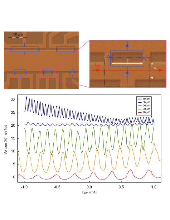
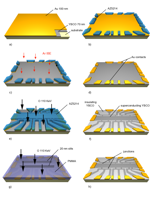
Starting from a commercial 70 nm thick (YBCO) film ( = 86 K) grown on sapphire covered by an in-situ 100 nm gold layer, a three steps fabrication process is performed. Firstly, contact pads are defined in the gold layer through optical photoresist patterning followed by a 500 eV Ar Ion Beam Etching (IBE). Secondly, contact lines and SQUIDs arms are patterned in a AZ5214 image-reversal photoresist followed by 110 keV oxygen ions irradiation. A dose of ions/cm ensures that the surrounding matrix is deeply insulating. Eventually, Josephson junctions are fabricated : 20 nm slits in a 600 nm thick poly(methylmethacrylate) (PMMA) photoresist are patterned using a LEICA EBPG 5000+ electronic beamwriter and irradiated with 110 keV oxygen ions. We used a dose of ions/cm suitable to operate in the temperature range 40 to 65 K. Different geometries for the SQUIDs arms carrying the injection current have been studied : width of 4 μm and 10 μm, and five different lengths for each width : 10, 20, 30, 50 and 80 μm. 1 displays the layout of a typical sample showing five different SQUIDs (width of 10 μm and lengths from 10 to 80 μm) sharing a common ground electrode, together with current injection lines.
Measurements were conducted in an Oxford Variable Temperature Insert using four-probe method and two extra-leads on one electrode of SQUIDs for current injection in the superconducting wire (Upper right panel of 1). After measuring the critical current as a function of T, the SQUID was biased at its optimal point ( ) while the control current was swept. This results in oscillations in the SQUID’s voltage (Lower panel in 1) with a current periodicity that can be related to the inductance of the superconducting line through the simple formula where Wb is the magnetic flux quantum and the inductance of the superconducting lineHasegawa et al. (1995); Il’ichev et al. (1996); Fuke et al. (1996); Terai et al. (1997); Johansson et al. (2009).

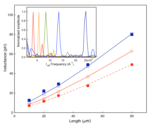
A first set of data was extracted from SQUIDs with highly irradiated junctions measured at 4.2 K in order to extract the zero temperature London penetration depth . The injection current was swept from -1 mA to 1 mA giving 20 to 50 oscillations of the SQUID voltage which were enough for reliably Fourier transform the data as displayed in the inset of 2. The corresponding inductances (solid symbols) are displayed in 2 for the two widths as a function of the SQUID arm nominal length. As expected, the total inductance increases slightly more rapidly than linearly, since it is the sum of the kinetic contribution Duzer and Turner (1998) and the geometric one Grover (1946), where is the London penetration depth and the thickness of the film. A more accurate estimate of has been computed with the 3D-MLSI software Khapaev and Goldobin (2004) on the actual geometry of the SQUIDs (dashed line of figure 1). The results are given as open symbols in 2. The agreement for the 4 μm wide superconducting lines is very good given the zero temperature μm, which is exactly the film supplier’s data, thus indicating that our fabrication process preserves the superconducting properties of the films. Concerning the 10 μm wide superconducting lines, the numerical simulations needs to be renormalized by a factor of to yield to correct results (dashed line in 2). This numerical factor accounts for all the measured samples with this geometry. We do not have a clear explanation for this 20% discrepancy. However we should stress that most of the reported data in the literature using this DC SQUID method, do not provide quantitative agreements between measured and calculated inductances with such a precision.

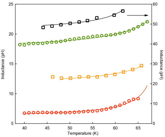
The second set of SQUIDs were operated in the temperature range of interest 40-65 K and allowed us to extract the temperature dependence of the London penetration depth. The injection current was swept up to 10 mA to give the precision needed to measure the slight variation in inductance with temperature. 3 summarizes our results together with fits of the temperature dependence of the inductance controlled by the penetration depth. Here we have used the Gorter-Casimir two fluids models with an exponent α = 2: Il’ichev et al. (1996); Terai et al. (1997); Johansson et al. (2009). Given the values = 0.135 μm and = 0.78 measured previously for the 10 μm wide sample, we found a good agreement providing that is adjusted within 5 K or so (see caption of 3). This uncertaincy has two origins related to the measurement method itself. Firstly, the Josephson regime of the irradiated junctions is limited in temperatureBergeal et al. (2005). Therefore, our measurements are restricted in a temperature range (40-65 K in this case) well below the bulk , in a region where does not strongly vary. Secondly, as the sensitivity of the measurement decreases when we approach this coupling temperature, one has to use high current density exceeding 10 A/cm , that is the critical one in our samples at 77 K. The actual in the wire might therefore be lowered.
The overall measurements of inductances give us a value of 0.6 pH/μm for a 10 μm wide line and 0.9 pH/μm for a 4 μm wide line. These numbers compare favorably with the best one reported in the literature Terai et al. (1997). They do not change if the strip-line is embedded in a coplanar wave guide geometry with a typical gap of 4 μm with respect to the ground plane. However, a factor of three improvement is expected when a ground plane is added Forrester et al. (1994); Terai et al. (1997). Such a desirable situation could be realized by adapting the ion irradiation process to trilayer films Bergeal et al. (2007, 2008).
Ion-irradiated junctions have typical critical current values in the range 100 μA - 1 mA which leads to a screening parameter ranging between 0.6 and 6 for a 10 μm long and wide strip, or 0.36 and 3.6 for a 4 μm one. Since RSFQ logic requires screening parameters around 1 for transmission lines and around 3 for storage cell Gueret et al. (1980); Likharev and Semenov (1991), the above mentioned inductances values fit well. Therefore, the irradiated junction technology seems suitable for RSFQ circuits applications.
In conclusion, we have measured the inductance of YBCO strip lines
made by ion irradiation using direct current injection in SQUIDs arms.
The measured values agree well with the calculated one using 3D simulation
of our circuits. Such a line inductance combined with the typical
critical currents of ion irradiated Josephson Junctions opens the
route towards the realization of RSFQ logic circuits using this new
technology.
This work has been supported by the Region Ile-de-France in the framework of C’Nano IdF and by the D l gation G n rale de l’Armement (DGA) through a doctoral grant. C’Nano IdF is the nanoscience competence center of Paris Region, supported by CNRS, CEA, MESR and Region Ile-de-France. Authors would like to thank Y. Legall at INESS Strasbourg for the ion irradiations.
References
- Bedard et al. (2005) F. Bedard, N. K. Welker, G. R. Cotter, M. A. Escavage, and J. T. Pinkston, National Security Agency Office of Corporate Assessments (2005).
- Silver et al. (2003) A. Silver, A. Kleinsasser, G. Kerber, Q. Herr, M. Dorojevets, P. Bunyk, and L. Abelson, Superconductor Science and Technology, 16, 1368 (2003).
- Fujimaki et al. (2008) A. Fujimaki, M. Tanaka, T. Yamada, Y. Yamanashi, H. Park, and N. Yoshikawa, IEICE Transactions on Electronics, E91-C, 342 (2008).
- ter Brake et al. (2008) H. ter Brake, F.-I. Buchholz, G. Burnell, T. Claeson, D. Créte, P. Febvre, G. Gerritsma, H. Hilgenkamp, R. Humphreys, Z. Ivanov, W. Jutzi, M. Khabipov, J. Mannhart, H.-G. Meyer, J. Niemeyer, A. Ravex, H. Rogalla, M. Russo, J. Satchell, M. Siegel, H. Töpfer, F. Uhlmann, J.-C. Villégier, E. Wikborg, D. Winkler, and A. Zorin, Physica C, 439, 1 (2008).
- Tanabe et al. (2008) K. Tanabe, H. Wakana, K. Tsubone, Y. Tarutani, S. Adachi, Y. Ishimaru, M. Maruyama, T. Hato, A. Yoshida, and H. Suzuki, IEICE Trans. Electron., E91-C, 280 (2008).
- Bergeal et al. (2005) N. Bergeal, X. Grison, J. Lesueur, G. Faini, M. Aprili, and J. Contour, Applied Physics Letters, 87, 102502 (2005).
- Bergeal et al. (2006) N. Bergeal, J. Lesueur, G. Faini, M. Aprili, and J. P. Contour, Applied Physics Letters, 89, 112515 (2006).
- Bergeal et al. (2007) N. Bergeal, J. Lesueur, M. Sirena, G. Faini, M. Aprili, J. P. Contour, and B. Leridon, J Appl Phys, 102, 083903 (2007).
- Cybart et al. (2009) S. A. Cybart, S. M. Anton, S. M. Wu, J. Clarke, and R. C. Dynes, Nano Lett, 9, 3581 (2009).
- Hasegawa et al. (1995) H. Hasegawa, Y. Tarutani, T. Fukazawa, U. Kabasawa, and K. Takagi, Applied Physics Letters, 67, 3177 (1995).
- Il’ichev et al. (1996) E. Il’ichev, L. Dörrer, F. Schmidl, and V. Zakosarenko, Applied Physics … (1996).
- Fuke et al. (1996) H. Fuke, K. Saitoh, T. Utagawa, and Y. Enomoto, Japanese Journal Of Applied Physics, 35, 1582 (1996).
- Terai et al. (1997) H. Terai, M. Hidaka, T. Satoh, and S. Tahara, Applied Physics Letters, 70, 2690 (1997).
- Johansson et al. (2009) J. Johansson, K. Cedergren, and T. Bauch, Physical Review B (2009).
- Duzer and Turner (1998) T. V. Duzer and C. Turner, New York: Elsevier North Holland, Principles of Superconductive Devices and Circuits (1998).
- Grover (1946) F. Grover, New York: Dover Publications, Inductance calculations - Working Formulas and Tables (1946).
- Khapaev and Goldobin (2004) M. Khapaev and E. Goldobin, http://www.cmc.msu.ru/vm/sotr/vmhap, 3D-MLSI : The program for extraction of 3D inductances of multilayer superconductor circuits (2004).
- Forrester et al. (1994) M. Forrester, A. Davidson, J. Talvacchio, J. Gavaler, and J. Przybysz, Applied Physics Letters, 65, 1835 (1994).
- Bergeal et al. (2008) N. Bergeal, J. Lesueur, M. Aprili, G. Faini, J. P. Contour, and B. Leridon, Nature Physics, 4, 608 (2008).
- Gueret et al. (1980) P. Gueret, A. Moser, and P. Wolf, IBM Journal of Research and Development, 24, 155 (1980).
- Likharev and Semenov (1991) K. K. Likharev and V. K. Semenov, IEEE Trans. Appl. Supercond., 1, 280 (1991).
