Gate-controlled guiding of electrons in graphene
Ballistic semiconductor structures have allowed the realization of optics-like phenomena in electronics, including magnetic focusing Houten89 and lensing Sivan90 . An extension that appears unique to graphene is to use both and carrier types to create electronic analogs of optical devices having both positive and negative indices of refraction Cheianov07 . Here, we use gate-controlled density with both and carrier types to demonstrate the analog of the fiber-optic guiding in graphene Beenakker09 ; Zhang09 ; Villegas10 ; He10 ; Wu10 . Two basic effects are investigated: (1) bipolar p-n junction guiding, based on the principle of angle-selective transmission though the graphene p-n interface, and (2) unipolar fiber-optic guiding, using total internal reflection controlled by carrier density. Modulation of guiding efficiency through gating is demonstrated and compared to numerical simulations, which indicates that interface roughness limits guiding performance, with few-nanometer effective roughness extracted. The development of p-n and fiber-optic guiding in graphene may lead to electrically reconfigurable wiring in high-mobility devices.

Graphene is a single layer hexagonal lattice of carbon atoms with a gapless, linear dispersion that leads to novel electronic properties CastroNeto09 ; Beenakker08 . Carrier type and density can be controlled via gates, creating high-mobility, bipolar graphene electronics Geim09 . Electronic transport across an interface of holes () and electrons () - a p-n junction - has been studied experimentally using a combination of top/bottom electrostatic gates to create and regions Huard07 ; Williams07 ; Ozyilmaz07 , and is now well understood theoretically Cheianov06 ; Katsnelson06 ; Low09 ; Stander09 ; Young09 .
An intriguing possibility is to use both and carrier types in bipolar graphene structures to create electronic analogs of optical devices having both positive and negative indices of refraction. For example, a symmetrically biased p-n junction has been shown theoretically to create a negative refractive index medium analogous to a Veselago lens Cheianov07 . Such a device is not possible using conventional two-dimensional electron gas (2DEG) systems, and demonstrates a unique feature of a Dirac-like band structure in conjunction with the ability to electrostatically tune between and carrier types. There is considerable theoretical interest in using the Dirac-like properties of graphene to create novel optical devices in graphene Beenakker09 ; Zhang09 ; Villegas10 ; He10 ; Wu10 ; Park08 ; Low09b ; Hartmann10 ; Mischenko10 ; Cesar10 , but experiments on these systems have not yet been reported.
In this Letter, we demonstrate experimentally and numerically the graphene analog of a well-known optical device, the fiber optic. Three regimes of current guiding are identified in the experiment and simulations: (1) p-n junction guiding, based on the principle of angle-selective transmission, (2) the graphene fiber-optic analog, using total internal reflection and (3) an mixture of the two effects. A metric of the guiding efficiency is predicted in all three regimes. By varying the external parameters of gate voltage and magnetic field, guiding efficiencies in each regime are extracted from experiment, where trends in the parameters are observed and compared to numerical simulations.
Photons and electrons exhibit analogous wave phenomena, reflected in the similarity of the Helmholtz equation describing electromagnetic wave propagation and the Schrödinger equations describing propagation for electrons Dragoman99 ; Wilson93 . In graphene, the Fermi energy () plays the role of index of refraction in an optical medium Cheianov07 ; Beenakker09 ; Zhang09 ; Villegas10 ; He10 ; Wu10 , with the important feature that can be modified via electrostatic gates. We note that the dependence of the effective index of refraction on density and gate voltage in graphene differs from the dependence in conventional 2DEGs. In graphene, the wave number, and hence the effective index, is proportional to . In conventional 2DEGs, the wave number and effective index scale as Sivan90 . More significantly, for graphene, can either be positive (for electrons) or negative (for holes).
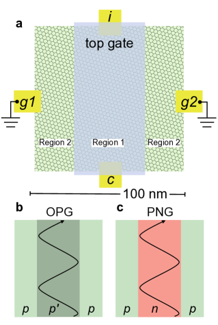
For the device shown schematically in Fig. 1a, the effective index of refraction under the top gate (Region 1), , is controlled by the combined voltages on the top gate, , and backgate, , while the effective index of refraction outside the top-gated region (Region 2), , is controlled only by . When , the device operates as an electronic fiber optic with critical angle =, This effect, termed optical guiding (OPG), is shown schematically in Fig. 1b. Modes propagating with will be totally internally reflected and therefore travel down the channel without leaking out of the fiber.
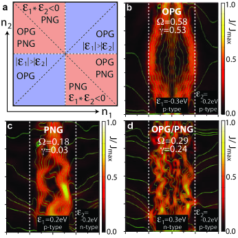
Transmission across a graphene p-n interface decreases exponentially with angle from the interface normal Cheianov06 . Therefore at grazing incidence, nearly all carriers impinging on the p-n interface are reflected, which leads to guiding of all but a small number of carriers. This guiding mechanism is termed p-n guiding (PNG) and is shown schematically in Fig. 1c. Depending on values of and , the mechanism responsible for guiding will be either OPG, p-n -junction guiding (PNG) or a combination of the two (OPG/PNG). The carrier-density location of these three regions are shown as a function of the density underneath the top gate () and outside the top gate () in Fig. 2a. For unipolar devices (no p-n junctions, shaded blue), only OPG is present. For bipolar devices (shaded red), both PNG and OPG/PNG can occur. OPG occurs if ; PNG occurs if ; OPG/PNG occurs if both conditions are satisfied.
Quantum transport simulations are used to extract guiding efficiency as a function of gate voltages (see Supp. Info. for numerical methods). The simulated device (Fig. 1a) has four contacts, (injector), (collector), , and (electrical ground 1, 2) (Fig. 1a). Guiding efficiency is defined as the fraction of current collected at due to injection from , , where is the transmission probability from contact to , and . Note that is finite even for equal indices of refraction in regions 1 and 2, since is nonzero when i.e. a uniformly-biased graphene sheet. We therefore define as the difference between and its value for equal indices,
| (1) |
The parameter then serves as an effective measure of the guiding efficiency due to unequal indices of refraction for the graphene channel, independent of the source of guiding. The condition follows from particle-hole symmetry. We take Fermi energy to be equivalent to the effective index of refraction, and so equate and with Fermi energies in regions 1 and 2.

Simulations for a 100 100 device (matching the experimental geometry) in the OPG, PNG and OPG/PNG regimes (Fig. 2b-d), yield guiding efficiencies for OPG, for PNG, and for OPG/PNG. Using =0.05 (Fig. 2b and d) and =0.15 (Fig. 2c) gives for OPG, for PNG, and for OPG/PNG. To obtain these values, simulations assumed a root-mean-square interface roughness of 4 nm in the p-n case and no roughness in the p-p interface. Adding roughness is neccessary to obtain the qualitative trend observed experimentally, ; without interface roughness for the p-n case, numerics gave . The larger roughness in the p-n regime presumably reflecting the poor screening of disorder at the zero-density p-n junction Zhang08 and consistent with the theoretical observation that large-angle-scattering modes are deteriorated by disorder Rossi10 . For p-p interface, a larger than experiments is obtained when assuming an ideal p-p interface. It is therefore necessary to also add some roughness to the p-p interface to obtain quantitative agreement with experiment, as seen in Fig. 3.
We next discuss the experimental realization of electron guiding. Devices were made from mechanical exfoliation of highly-oriented pyrolytic graphite. Metallic contacts (, , and ) were patterned with electron-beam lithography (see Fig 1a), and the size of device was reduced to 100 100 using an O2/Ar2 plasma etch, giving a device of dimensions comparable to its mean-free path, determined by transport. A functionalized, top-gate oxide was grown Williams07 and a top-gate electrode patterned using electron-beam lithography. Differential resistance was measured using a standard lock-in technique at a temperature T=30 K. Relatively high temperature and large densities were used to suppress Coloumb blockade fluctuations of the resistance present in the small device at low temperatures and densities. The field-effect, Drude mean free path , where , for micron-sized graphene sheets is routinely found to be away from the charge-neutrality point. Here, however, it is difficult to estimate in these submicron devices, as the charging energy will create deviations from the simple Drude model. Extracting from a four-terminal measurement yields 70 nm. Given the limitations of the Drude , the device is at very least in the quasi-ballistic regime.
Experimental guiding efficiency is determined from transport measurements . Transmission is obtained in a “channel” geometry, with current applied to , and , , and grounded, from the resistance ,
| (2) |
Transmission is measured in a “focusing” geometry Houten89 , with current applied to , voltage measured at , and and grounded. Using this geometry, two resistances are measured by monitoring the voltages at contacts and : and . A calculation of could be made by taking the ratio of these two resistances, however, the symmetry and , may not hold in real devices. Accounting for deviation from above idealities, we average over the two configurations and to obtain a value for guiding in terms of resistances and (see Supplementary information),
| (3) |
where the two terms in Eq. 3 are and respectively. Ideally, the symmetry of the device would entails and and Eq. 3 would reduce to . However, this will not be the case in typical experimental condition due to disorder and contact misalignment. A quantitative estimation of the experimental guiding efficiency is obtained by taking the average of and , producing Eq. 3. Since , one also has the inequalities , and , in agreement with experiment (see Supplementary information).

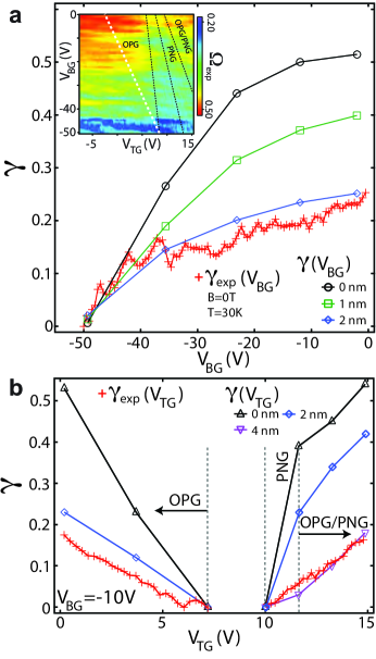
Values for as a function of top and back gate voltages, extracted , and , are shown in the inset of Fig. 3, along with boundaries of the guiding regimes based on the boundaries in Fig. 2a. is maximal in the OPG and OPG/PNG regimes, and follows the pattern .
Experimental and numerical results for guiding efficiency are compared in the OPG regime, where guiding is most efficient, along a cut at constant density (Fermi energy 0.3 eV) in Region 1, indicated by the white dashed line in the inset of Fig. 3. Experimental guiding efficiency along this cut is obtained from by subtracting 0.3 eV, 0.3 eV)=0.26. Figure 3 shows as a function of in the OPG regime along with numerical results for eV with numerical interface roughnesses of 0, 1, and 2 nm. Numerical values of were computed from using 0.3 eV, 0.3 eV)=0.05. For all values of interface roughness, increases with increasing (or decreasing ), and good quantitative agreement with experiment is found for a roughness of 2 nm. The dependence of on can be understood by analogy with optical fiber, where decreasing the refractive index in the fiber cladding leads to smaller critical angle. The inset of Fig. 3 shows that the trend of increasing with back-gate voltage is more prominent in the OPG regime than in the PNG regime. This is consistent with expectation, as the effect of in the PNG regime is mostly to change the location of the p-n interface, where reflection occurs; transparency of the p-n interface itself is not strongly affected by , as it is in the OPG regime.
is also extracted at =-10 V, showing guiding in the OPG, PNG and OPG/PNG regimes (red crosses in Fig. 3b). Values for the “equal-episilon” background subtraction were extracted experimentally for the OPG regime, while the PNG and OPG/PNG values were inferred from the extracted value using particle-hole symmetry (i.e. ) as in Fig. 2. In the OPG regime, falls roughly linearly as a fucntion of from 0.18 to 0, while in the PNG and OPG/PNG regimes it rises from 0.01 to 0.16. For between 7 V and 10 V, in not define as it does not satisfy the conditions for guiding (see Fig. 2a). Numerical simulations for this value of are shown for the 3 regimes for 3 different amounts of disorder: 0 (black), 2 (blue) and 4 nm (purple). Here we see good agreement between and in the OPG for 2 nm of disorder, similar to Fig. 3a. However 2 nm of interface disorder is clearly off in the PNG and OPG/PNG regimes, and more disorder (4 nm) is needed to obtain agreement between experiment and simulations. This is consistent with the argument of poor screening at the p-n interface used in the PNG and OPG/PNG regimes in Fig. 2.

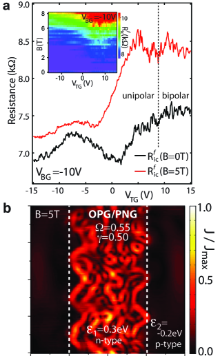
Transparency across a graphene p-n junction decreases with applied perpendicular magnetic field (B), as discussed theoretically by Refs. Cheianov06 ; Shytov09 , and seen experimentally in Ref. Huard07 . The reduced transparency in a magnetic field increases guiding efficiency, as demonstrated experimentally in Fig. 4. When — the experimentally relevant case, see Fig. S1 in the Supp. Info—. () at B=5 T is compared to the zero-field value in Fig. 4a. At =-10 V an increase of 0.1 k in the unipolar regime and 1 k in the bipolar regime as B is increase to 5 T is observed. The inset of Fig. 4a shows ,B), where an enhancement in resistance is apparent for B2 T. Since the ratio increases with B, we ascribe the enhancement in (and, by inference, an increase in ) as a result of an increase in the PNG contribution to current guiding. Fig. 4b shows the simulated current density with B=5 T, showing an improved guiding efficiency of () from the B=0 value of () [see Fig. 2d for B=0 value].
In summary, we have investigated electron guiding in graphene by tuning the carrier type and density using local electrostatic fields to create the analogue of an optical fiber. Guiding efficiency was extracted in three regimes: in the unipolar OPG regime, where the device is analogous to a fiber optic; in the bipolar PNG regime, where guiding occurs because of reflection at p-n interfaces; and the bipolar OPG/PNG regime, where both mechanisms operate. We also demonstrated experimentally that guiding efficiency increases with an applied perpendicular magnetic field, consistent with numerical results. One would expect that pseudomagnetic fields created by strain engineering Guinea09 of greater than 300 T Levy10 can also enhance guiding. Improvements to guiding efficiency will result from reducing interface disorder. Engineering of a collimated source with modes within the acceptance cone of the fiber would also improves guiding. With such improvements, this approach could perhaps lead to electrically reconfigurable wiring using graphene.
References
- (1) van Houten, H. et al., Coherent electron focusing with quantum point contacts in a two-dimensional electron gas. Phys. Rev. B 39, 8556-8575 (1989).
- (2) Sivan, U., Heiblum, M., Umbach, C. P., & Strickman, H. Electrostatic electron lens in the ballistic regime. Phys. Rev. B 41, 7937-7940 (1990).
- (3) Cheianov, V. V., Fal’ko, V. I., & Altshuler, B.L. The Focusing of Electron Flow and a Veselago Lens in Graphene p-n Junctions. Science 315, 1252-1255 (2007).
- (4) Beenakker, C. W. J., Sepkhanov, R. A., Akhmerov, A. R., & Tworzydlo, J. Quantum Goos-Hänchen Effect in Graphene. Phys. Rev. Lett. 102, 146804 (2009).
- (5) Zhang, F.- M., He, Y., & Chen, X., Guided Modes in graphene waveguides. Appl. Phys. Lett. 94, 212105 (2009).
- (6) Villegas, C. E. P & Tavares, R. S., Comment on “Guided modes in graphene waveguides” [Appl. Phys. Lett. 94, 212105 (2009)]. Appl. Phys. Lett. 96, 186101 (2010).
- (7) He, Y., Zhang, F.- M., & Chen, X. Response to “Comment on ‘Guided modes in graphene waveguides’ ” [Appl. Phys. Lett. 96, 186101 2010]. Appl. Phys. Lett. 96, 186102 (2010).
- (8) Wu, Zhenhua. Electronic fibre in graphene. arXiv:1008.2495 (2010).
- (9) Castro Neto, A. H. et al.. The electronic properties of graphene. Rev. Mod. Phys. 81, 109-162 (2009).
- (10) C. W. J. Beenakker. Colloquium: Andreev reflection and Klein tunneling in graphene. Rev. Mod. Phys. 80, 1337-1354 (2008).
- (11) Geim, A. K. Graphene: Status and Prospects. Science 324, 1530-1534 (2009).
- (12) Huard, B. et al. Transport Measurements Across a Tunable Potential Barrier in Graphene. Phys. Rev. Lett. 98, 236803 (2007).
- (13) Williams, J. R., DiCarlo, L., & Marcus, C. M. Quantum Hall Effect in a Gate-Controlled p-n Junction of Graphene. Science 317, 638-641 (2007).
- (14) Özyilmaz, B. et al. Electronic Transport and Quantum Hall Effect in Bipolar Graphene p-n-p Junctions. Phys. Rev. Lett. 99, 166804 (2007).
- (15) Cheianov, V. V. & Fal’ko, V. I. Selective transmission of Dirac electrons and ballistic magnetoresistance of n-p junctions in graphene. Phys. Rev. B 74, 041403(R) (2006).
- (16) Katsnelson, M. I., Novoselov, K. S., & Geim, A. K. Chiral tunnelling and the Klein paradox in graphene. Nature Phys. 2 620-625 (2006).
- (17) Low, T., Hong, S., Appenzeller, J., Datta, S., & Lundstrom, M. S. Conductance Asymmetry of Graphene p-n Junction. IEEE Trans. Elec. Dev. 56, 1292 (2009).
- (18) Stander, N., Huard, B., & Goldhaber-Gordon, D. Evidence for Klein Tunneling in Graphene p-n Junctions. Phys. Rev. Lett. 102, 026807 (2009).
- (19) Young, A. F. & Kim, P. Quantum interference and Klein tunnelling in graphene heterojunctions. Nature Phys. 5 222-226 (2009).
- (20) Park, C. H., Son, Y.-W., Yang, L., Cohen, M., & Louie, S. G. Electron Beam Supercollimation in Graphene Superlattices. Nano Lett. 8, 2920-2924 (2008).
- (21) Low, T. & Appenzeller, J. Electronic transport properties of a tilted graphene p-n junction. Phys. Rev. B 80, 155406 (2009).
- (22) Hartmann, R. R., Robinson, N. J., & Portnoi, M. E. Smooth electron waveguides in graphene. Phys. Rev. B 81, 245431 (2010).
- (23) Mishchenko, E. G., Shytov, A.V., & Silvestrov, P. G. Guided Plasmons in Graphene p-n Junctions. Phys. Rev. Lett. 104, 156806 (2010).
- (24) Cesar, E. P, Villegas, M. & Tavares, R. S. Strongly coupled modes in bi-waveguides based on graphene. Solid State Commun. 150, 1350 (2010).
- (25) D. Dragoman & M. Dragoman, Quantum-Classical Analogies (Spinger, Heidelberg, 2004).
- (26) Wilson, D. W., Glytsis, E. N. & Gaylord, T. K. Electron waveguiding characteristics and ballistic current capacity of semiconductor quantum slabs. IEEE J. Quant. Electron. 29 1364 (1993).
- (27) Zhang, L. M. & Fogler, M. M. Nonlinear Screening and Ballistic Transport in a Graphene p-n Junction. Phys. Rev. Lett. 100, 116804 (2008).
- (28) E. Rossi, J. H. Bardarson, P. W. Brouwer, and S. Das Sarma Signatures of Klein tunneling in disordered graphene p-n-p junctions. Phys. Rev. B 81 121408(R) (2010).
- (29) Shytov, A., Rudner, M. S., & Levitov, L. S. Klein Backscattering and Fabry-Pérot Interference in Graphene Heterojunctions. Phys. Rev. Lett. 101, 156804 (2008).
- (30) Guinea, F., Katsnelson, M. I., & Geim, A. K. Energy gaps and a zero-field quantum Hall effect in graphene by strain engineering. Nat. Phys. 6, 30-33 (2009).
- (31) Levy, N. et al. Strain-Induced Pseudo Magnetic Fields Greater Than 300 Tesla in Graphene Nanobubbles. Science 329, 544-547 (2010).
Device fabrication was done using Harvard’s Center for Nanoscale Systems (CNS), a member of the National Nanotechnology Infrastructure Network (NNIN) under NSF award ECS-0335765, and was supported in part by INDEX, an NRI Center, and the Harvard NSEC.